1. General
description
The LPC1759/58/56/54/52/51 are ARM Cortex-M3 based microcontrollers for embedded applications featuring a high level of integration and low power consumption. The ARM Cortex-M3 is a next generation core that offers system enhancements such as enhanced debug features and a higher level of support block integration.
The LPC1758/56/57/54/52/51 operate at CPU frequencies of up to 100 MHz. The LPC1759 operates at CPU frequencies of up to 120 MHz. The ARM Cortex-M3 CPU incorporates a 3-stage pipeline and uses a Harvard architecture with separate local instruction and data buses as well as a third bus for peripherals. The ARM Cortex-M3 CPU also includes an internal prefetch unit that supports speculative branching.
The peripheral complement of the LPC1759/58/56/54/52/51 includes up to 512 kB of flash memory, up to 64 kB of data memory, Ethernet MAC, USB Device/Host/OTG interface, 8-channel general purpose DMA controller, 4 UARTs, 2 CAN channels, 2 SSP controllers,
SPI interface, 2 I2C-bus interfaces, 2-input plus 2-output I2S-bus interface, 6 channel
12-bit ADC, 10-bit DAC, motor control PWM, Quadrature Encoder interface, 4 general purpose timers, 6-output general purpose PWM, ultra-low power Real-Time Clock (RTC) with separate battery supply, and up to 52 general purpose I/O pins.
For additional documentation, see Section 19 “References”.
2. Features and benefits
ARM Cortex-M3 processor, running at frequencies of up to 100 MHz
(LPC1758/56/57/54/52/51) or of up to 120 MHz (LPC1759). A Memory Protection Unit (MPU) supporting eight regions is included.
ARM Cortex-M3 built-in Nested Vectored Interrupt Controller (NVIC).
Up to 512 kB on-chip flash programming memory. Enhanced flash memory accelerator
enables high-speed 120 MHz operation with zero wait states.
In-System Programming (ISP) and In-Application Programming (IAP) via on-chip
bootloader software.
On-chip SRAM includes:
Up to 32 kB of SRAM on the CPU with local code/data bus for high-performance
CPU access.
Two/one 16 kB SRAM blocks with separate access paths for higher throughput.
These SRAM blocks may be used for Ethernet (LPC1758 only), USB, and DMA memory, as well as for general purpose CPU instruction and data storage.
SRAM with Ethernet, USB 2.0 Host/Device/OTG, CAN
Eight channel General Purpose DMA controller (GPDMA) on the AHB multilayer
matrix that can be used with the SSP, I2S-bus, UART, the Analog-to-Digital and
Digital-to-Analog converter peripherals, timer match signals, and for memory-to-memory transfers.
Multilayer AHB matrix interconnect provides a separate bus for each AHB master.
AHB masters include the CPU, General Purpose DMA controller, Ethernet MAC (LPC1758 only), and the USB interface. This interconnect provides communication with no arbitration delays.
Split APB bus allows high throughput with few stalls between the CPU and DMA.
Serial interfaces:
On the LPC1758 only, Ethernet MAC with RMII interface and dedicated DMA
controller.
USB 2.0 full-speed device/Host/OTG controller with dedicated DMA controller and
on-chip PHY for device, Host, and OTG functions. The LPC1752/51 include a USB device controller only.
Four UARTs with fractional baud rate generation, internal FIFO, and DMA support.
One UART has modem control I/O and RS-485/EIA-485 support, and one UART has IrDA support.
CAN 2.0B controller with two (LPC1759/58/56) or one (LPC1754/52/51) channels.
SPI controller with synchronous, serial, full duplex communication and
programmable data length.
Two SSP controllers with FIFO and multi-protocol capabilities. The SSP interfaces
can be used with the GPDMA controller.
Two I2C-bus interfaces supporting fast mode with a data rate of 400 kbit/s with
multiple address recognition and monitor mode.
On the LPC1759/58/56 only, I2S (Inter-IC Sound) interface for digital audio input or
output, with fractional rate control. The I2S-bus interface can be used with the
GPDMA. The I2S-bus interface supports 3-wire and 4-wire data transmit and
receive as well as master clock input/output.
Other peripherals:
52 General Purpose I/O (GPIO) pins with configurable pull-up/down resistors. All
GPIOs support a new, configurable open-drain operating mode. The GPIO block is accessed through the AHB multilayer bus for fast access and located in memory such that it supports Cortex-M3 bit banding and use by the General Purpose DMA Controller.
12-bit Analog-to-Digital Converter (ADC) with input multiplexing among six pins,
conversion rates up to 200 kHz, and multiple result registers. The 12-bit ADC can be used with the GPDMA controller.
On the LPC1759/58/56/54 only, 10-bit Digital-to-Analog Converter (DAC) with
dedicated conversion timer and DMA support.
Four general purpose timers/counters, with a total of three capture inputs and ten
compare outputs. Each timer block has an external count input. Specific timer events can be selected to generate DMA requests.
One motor control PWM with support for three-phase motor control.
Quadrature encoder interface that can monitor one external quadrature encoder.
One standard PWM/timer block with external count input.
Real-Time Clock (RTC) with a separate power domain and dedicated RTC
WatchDog Timer (WDT). The WDT can be clocked from the internal RC oscillator, the RTC oscillator, or the APB clock.
ARM Cortex-M3 system tick timer, including an external clock input option.
Repetitive Interrupt Timer (RIT) provides programmable and repeating timed
interrupts.
Each peripheral has its own clock divider for further power savings.
Standard JTAG debug interface for compatibility with existing tools. Serial Wire Debug
and Serial Wire Trace Port options. Boundary scan Description Language (BSDL) is not available for this device.
Emulation trace module enables non-intrusive, high-speed real-time tracing of
instruction execution.
Integrated PMU (Power Management Unit) automatically adjusts internal regulators to
minimize power consumption during Sleep, Deep sleep, Power-down, and Deep power-down modes.
Four reduced power modes: Sleep, Deep-sleep, Power-down, and Deep power-down.
Single 3.3 V power supply (2.4 V to 3.6 V).
One external interrupt input configurable as edge/level sensitive. All pins on Port 0 and
Port 2 can be used as edge sensitive interrupt sources.
Non-maskable Interrupt (NMI) input.
The Wakeup Interrupt Controller (WIC) allows the CPU to automatically wake up from
any priority interrupt that can occur while the clocks are stopped in Deep sleep, Power-down, and Deep power-down modes.
Processor wake-up from Power-down mode via any interrupt able to operate during
Power-down mode (includes external interrupts, RTC interrupt, USB activity, Ethernet wake-up interrupt (LPC1758 only), CAN bus activity, Port 0/2 pin interrupt, and NMI).
Brownout detect with separate threshold for interrupt and forced reset.
Power-On Reset (POR).
Crystal oscillator with an operating range of 1 MHz to 25 MHz.
4 MHz internal RC oscillator trimmed to 1 % accuracy that can optionally be used as a
system clock.
PLL allows CPU operation up to the maximum CPU rate without the need for a
high-frequency crystal. May be run from the main oscillator, the internal RC oscillator, or the RTC oscillator.
USB PLL for added flexibility.
Code Read Protection (CRP) with different security levels.
Unique device serial number for identification purposes.
Available as 80-pin LQFP package (12 mm 12 mm 1.4 mm).
3. Applications
eMetering Lighting Industrial networking Alarm systems White goods Motor control4. Ordering
information
4.1 Ordering options
Table 1. Ordering information
Type number Package
Name Description Version
LPC1759FBD80 LQFP80 plastic low-profile quad package; 80 leads; body 12 12 1.4 mm SOT315-1 LPC1758FBD80 LQFP80 plastic low-profile quad package; 80 leads; body 12 12 1.4 mm SOT315-1 LPC1756FBD80 LQFP80 plastic low-profile quad package; 80 leads; body 12 12 1.4 mm SOT315-1 LPC1754FBD80 LQFP80 plastic low-profile quad package; 80 leads; body 12 12 1.4 mm SOT315-1 LPC1752FBD80 LQFP80 plastic low-profile quad package; 80 leads; body 12 12 1.4 mm SOT315-1 LPC1751FBD80 LQFP80 plastic low-profile quad package; 80 leads; body 12 12 1.4 mm SOT315-1
Table 2. Ordering options
Ty p e n u m b e r De vice or der p a rt numbe r Fl as h (k B) SRAM in kB
Ethernet USB CAN 2IS-bus DAC GPI
O Max imum CPU op era tin g freq ue nc y (MHz) CPU AHB SRAM0 AHB SRAM1 To ta l
LPC1759FBD80 LPC1759FBD80,551 512 32 16 16 64 no Device/Host/OTG 2 yes yes 52 120 LPC1758FBD80 LPC1758FBD80Y 512 32 16 16 64 yes Device/Host/OTG 2 yes yes 52 100 LPC1756FBD80 LPC1756FBD80/CP327 256 16 16 - 32 no Device/Host/OTG 2 yes yes 52 100 LPC1754FBD80 LPC1754FBD80,551 128 16 16 - 32 no Device/Host/OTG 1 no yes 52 100 LPC1752FBD80 LPC1752FBD80,551 64 16 - - 16 no Device only 1 no no 52 100 LPC1751FBD80 LPC1751FBD80,551 32 8 - - 8 no Device only 1 no no 52 100
5. Marking
The LPC175x devices typically have the following top-side marking: LPC175xxxx
xxxxxxx xxYYWWR[x]
The last/second to last letter in the third line (field ‘R’) will identify the device revision. This data sheet covers the following revisions of the LPC175x:
Field ‘YY’ states the year the device was manufactured. Field ‘WW’ states the week the device was manufactured during that year.
Table 3. Device revision table
Revision identifier (R) Revision description
‘-’ Initial device revision
6. Block
diagram
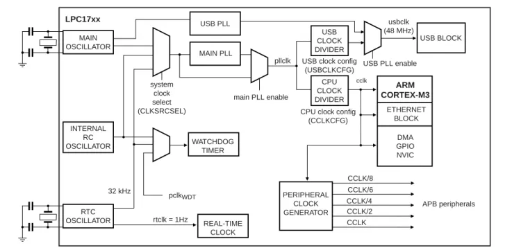
Grey-shaded blocks represent peripherals with connection to the GPDMA. Fig 1. Block diagram
SRAM 64/32/ 16/8 kB ARM CORTEX-M3 TEST/DEBUG INTERFACE EMULA TION TRA CE MODULE FLASH ACCELERATOR FLASH 512/256/128/64/32 kB DMA CONTROLLER ETHERNET CONTROLLER WITH DMA(2) USB HOST/ DEVICE/OTG CONTROLLER WITH DMA(4) I-code bus D-code bus system bus AHB TO APB BRIDGE 0 HIGH-SPEED GPIO AHB TO APB BRIDGE 1 CLOCK GENERATION, POWER CONTROL, SYSTEM FUNCTIONS XTAL1 XTAL2 RESET clocks and controls JTAG interface debug port USB PHY SSP0 UART2/3 I2S(1) RI TIMER SYSTEM CONTROL SSP1 UART0/1 CAN1/CAN2(1) I2C1 SPI0 TIMER 0/1 WDT PWM1 12-bit ADC PIN CONNECT GPIO INTERRUPT CONTROL
RTC
BACKUP REGISTERS 32 kHz
OSCILLATOR
APB slave group 1 APB slave group 0
RTC POWER DOMAIN
LPC1759/58/56/54/52/51
master master master
002aae153 slave slave slave slave ROM slave slave MULTILAYER AHB MATRIX
P0, P1, P2, P4 SCK0 SSEL0 MISO0 MOSI0 SCK1 SSEL1 MISO1 MOSI1 RXD2/3 TXD2/3 SCL2 I2C2 SDA2 MOTOR CONTROL PWM MCOA[2:0] MCOB[2:0] MCI[2:0] TIMER2/3 4 × MAT2 2 × MAT3 I2SRX_SDA I2STX_CLK I2STX_WS I2STX_SDA TX_MCLK RX_MCLK DAC(3) AOUT
QUADRATURE ENCODER PHA, PHB
INDEX RTCX1 RTCX2 VBAT PWM1[6:1] 2 × MAT0/1 1 × CAP0, 2 × CAP1 RD1/2 TD1/2 SDA1 SCL1 AD0[7:2] SCK/SSEL MOSI/MISO 8 × UART1 RXD0/TXD0 P0, P2 PCAP1[1:0]
RMII pins USB pins
MPU
(1) LPC1759/58/56 only (2) LPC1758 only
EXTERNAL INTERRUPTS EINT0
(3) LPC1759/58/56/54 only (4) LPC1752/51 USB device only
7. Pinning
information
7.1 Pinning
7.2 Pin description
Fig 2. Pin configuration LQFP80 package
40 1 20 60 41 21 61 80 002aae158
Table 4. Pin description
Symbol Pin Type Description
P0[0] to P0[31] I/O Port 0: Port 0 is a 32-bit I/O port with individual direction controls for each bit. The operation of Port 0 pins depends upon the pin function selected via the pin connect block. Some port pins are not available on the LQFP80 package. P0[0]/RD1/TXD3/
SDA1
37[1] I/O P0[0] — General purpose digital input/output pin.
I RD1 — CAN1 receiver input.
O TXD3 — Transmitter output for UART3.
I/O SDA1 — I2C1 data input/output (this is not an I2C-bus compliant open-drain pin).
P0[1]/TD1/RXD3/ SCL1
38[1] I/O P0[1] — General purpose digital input/output pin.
O TD1 — CAN1 transmitter output. I RXD3 — Receiver input for UART3.
I/O SCL1 — I2C1 clock input/output (this is not an I2C-bus compliant open-drain pin).
P0[2]/TXD0/AD0[7] 79[2] I/O P0[2] — General purpose digital input/output pin.
O TXD0 — Transmitter output for UART0. I AD0[7] — A/D converter 0, input 7.
P0[3]/RXD0/AD0[6] 80[2] I/O P0[3] — General purpose digital input/output pin.
I RXD0 — Receiver input for UART0. I AD0[6] — A/D converter 0, input 6. P0[6]/
I2SRX_SDA/ SSEL1/MAT2[0]
64[1] I/O P0[6] — General purpose digital input/output pin.
I/O I2SRX_SDA — Receive data. It is driven by the transmitter and read by the receiver. Corresponds to the signal SD in the I2S-bus specification.
(LPC1759/58/56 only).
I/O SSEL1 — Slave Select for SSP1.
P0[7]/I2STX_CLK/ SCK1/MAT2[1]
63[1] I/O P0[7] — General purpose digital input/output pin.
I/O I2STX_CLK — Transmit Clock. It is driven by the master and received by the slave. Corresponds to the signal SCK in the I2S-bus specification.
(LPC1759/58/56 only).
I/O SCK1 — Serial Clock for SSP1.
O MAT2[1] — Match output for Timer 2, channel 1. P0[8]/I2STX_WS/
MISO1/MAT2[2]
62[1] I/O P0[8] — General purpose digital input/output pin.
I/O I2STX_WS — Transmit Word Select. It is driven by the master and received by the slave. Corresponds to the signal WS in the I2S-bus specification. (LPC1759/58/56
only).
I/O MISO1 — Master In Slave Out for SSP1. O MAT2[2] — Match output for Timer 2, channel 2. P0[9]/I2STX_SDA/
MOSI1/MAT2[3]
61[1] I/O P0[9] — General purpose digital input/output pin.
I/O I2STX_SDA — Transmit data. It is driven by the transmitter and read by the receiver. Corresponds to the signal SD in the I2S-bus specification.
(LPC1759/58/56 only).
I/O MOSI1 — Master Out Slave In for SSP1. O MAT2[3] — Match output for Timer 2, channel 3. P0[10]/TXD2/
SDA2/MAT3[0]
39[1] I/O P0[10] — General purpose digital input/output pin.
O TXD2 — Transmitter output for UART2.
I/O SDA2 — I2C2 data input/output (this is not an open-drain pin).
O MAT3[0] — Match output for Timer 3, channel 0. P0[11]/RXD2/
SCL2/MAT3[1]
40[1] I/O P0[11] — General purpose digital input/output pin.
I RXD2 — Receiver input for UART2.
I/O SCL2 — I2C2 clock input/output (this is not an open-drain pin).
O MAT3[1] — Match output for Timer 3, channel 1. P0[15]/TXD1/
SCK0/SCK
47[1] I/O P0[15] — General purpose digital input/output pin.
O TXD1 — Transmitter output for UART1. I/O SCK0 — Serial clock for SSP0. I/O SCK — Serial clock for SPI. P0[16]/RXD1/
SSEL0/SSEL
48[1] I/O P0[16] — General purpose digital input/output pin.
I RXD1 — Receiver input for UART1. I/O SSEL0 — Slave Select for SSP0. I/O SSEL — Slave Select for SPI. P0[17]/CTS1/
MISO0/MISO
46[1] I/O P0[17] — General purpose digital input/output pin.
I CTS1 — Clear to Send input for UART1. I/O MISO0 — Master In Slave Out for SSP0. I/O MISO — Master In Slave Out for SPI. P0[18]/DCD1/
MOSI0/MOSI
45[1] I/O P0[18] — General purpose digital input/output pin.
I DCD1 — Data Carrier Detect input for UART1. I/O MOSI0 — Master Out Slave In for SSP0. I/O MOSI — Master Out Slave In for SPI.
Table 4. Pin description …continued
P0[22]/RTS1/TD1 44[1] I/O P0[22] — General purpose digital input/output pin.
O RTS1 — Request to Send output for UART1. Can also be configured to be an RS-485/EIA-485 output enable signal.
O TD1 — CAN1 transmitter output. P0[25]/AD0[2]/
I2SRX _SDA/ TXD3
7[2] I/O P0[25] — General purpose digital input/output pin.
I AD0[2] — A/D converter 0, input 2.
I/O I2SRX_SDA — Receive data. It is driven by the transmitter and read by the receiver. Corresponds to the signal SD in the I2S-bus specification.
(LPC1759/58/56 only).
O TXD3 — Transmitter output for UART3. P0[26]/AD0[3]/
AOUT/RXD3
6[3] I/O P0[26] — General purpose digital input/output pin.
I AD0[3] — A/D converter 0, input 3.
O AOUT — DAC output. (LPC1759/58/56/54 only). I RXD3 — Receiver input for UART3.
P0[29]/USB_D+ 22[4] I/O P0[29] — General purpose digital input/output pin.
I/O USB_D+ — USB bidirectional D+ line.
P0[30]/USB_D 23[4] I/O P0[30] — General purpose digital input/output pin.
I/O USB_D — USB bidirectional D line.
P1[0] to P1[31] I/O Port 1: Port 1 is a 32-bit I/O port with individual direction controls for each bit. The operation of port 1 pins depends upon the pin function selected via the pin connect block. Some port pins are not available on the LQFP80 package.
P1[0]/ ENET_TXD0
76[1] I/O P1[0] — General purpose digital input/output pin.
O ENET_TXD0 — Ethernet transmit data 0. (LPC1758 only). P1[1]/
ENET_TXD1
75[1] I/O P1[1] — General purpose digital input/output pin.
O ENET_TXD1 — Ethernet transmit data 1. (LPC1758 only). P1[4]/
ENET_TX_EN
74[1] I/O P1[4] — General purpose digital input/output pin.
O ENET_TX_EN — Ethernet transmit data enable. (LPC1758 only). P1[8]/
ENET_CRS
73[1] I/O P1[8] — General purpose digital input/output pin.
I ENET_CRS — Ethernet carrier sense. (LPC1758 only). P1[9]/
ENET_RXD0
72[1] I/O P1[9] — General purpose digital input/output pin.
I ENET_RXD0 — Ethernet receive data. (LPC1758 only). P1[10]/
ENET_RXD1
71[1] I/O P1[10] — General purpose digital input/output pin.
I ENET_RXD1 — Ethernet receive data. (LPC1758 only). P1[14]/
ENET_RX_ER
70[1] I/O P1[14] — General purpose digital input/output pin.
I ENET_RX_ER — Ethernet receive error. (LPC1758 only). P1[15]/
ENET_REF_CLK
69[1] I/O P1[15] — General purpose digital input/output pin.
I ENET_REF_CLK — Ethernet reference clock. (LPC1758 only).
Table 4. Pin description …continued
P1[18]/ USB_UP_LED/ PWM1[1]/ CAP1[0]
25[1] I/O P1[18] — General purpose digital input/output pin.
O USB_UP_LED — USB GoodLink LED indicator. It is LOW when the device is configured (non-control endpoints enabled), or when the host is enabled and has detected a device on the bus. It is HIGH when the device is not configured, or when host is enabled and has not detected a device on the bus, or during global suspend. It transitions between LOW and HIGH (flashes) when the host is enabled and detects activity on the bus.
O PWM1[1] — Pulse Width Modulator 1, channel 1 output. I CAP1[0] — Capture input for Timer 1, channel 0. P1[19]/MCOA0/
USB_PPWR CAP1[1]
26[1] I/O P1[19] — General purpose digital input/output pin.
O MCOA0 — Motor control PWM channel 0, output A.
O USB_PPWR — Port Power enable signal for USB port. (LPC1759/58/56/54 only). I CAP1[1] — Capture input for Timer 1, channel 1.
P1[20]/MCI0/ PWM1[2]/SCK0
27[1] I/O P1[20] — General purpose digital input/output pin.
I MCI0 — Motor control PWM channel 0, input. Also Quadrature Encoder Interface PHA input.
O PWM1[2] — Pulse Width Modulator 1, channel 2 output. I/O SCK0 — Serial clock for SSP0.
P1[22]/MCOB0/ USB_PWRD/ MAT1[0]
28[1] I/O P1[22] — General purpose digital input/output pin.
O MCOB0 — Motor control PWM channel 0, output B.
I USB_PWRD — Power Status for USB port (host power switch). (LPC1759/58/56/54 only).
O MAT1[0] — Match output for Timer 1, channel 0. P1[23]/MCI1/
PWM1[4]/MISO0
29[1] I/O P1[23] — General purpose digital input/output pin.
I MCI1 — Motor control PWM channel 1, input. Also Quadrature Encoder Interface PHB input.
O PWM1[4] — Pulse Width Modulator 1, channel 4 output. I/O MISO0 — Master In Slave Out for SSP0.
P1[24]/MCI2/ PWM1[5]/MOSI0
30[1] I/O P1[24] — General purpose digital input/output pin.
I MCI2 — Motor control PWM channel 2, input. Also Quadrature Encoder Interface INDEX input.
O PWM1[5] — Pulse Width Modulator 1, channel 5 output. I/O MOSI0 — Master Out Slave in for SSP0.
P1[25]/MCOA1/ MAT1[1]
31[1] I/O P1[25] — General purpose digital input/output pin.
O MCOA1 — Motor control PWM channel 1, output A. O MAT1[1] — Match output for Timer 1, channel 1. P1[26]/MCOB1/
PWM1[6]/CAP0[0]
32[1] I/O P1[26] — General purpose digital input/output pin.
O MCOB1 — Motor control PWM channel 1, output B. O PWM1[6] — Pulse Width Modulator 1, channel 6 output. I CAP0[0] — Capture input for Timer 0, channel 0.
Table 4. Pin description …continued
P1[28]/MCOA2/ PCAP1[0]/ MAT0[0]
35[1] I/O P1[28] — General purpose digital input/output pin.
O MCOA2 — Motor control PWM channel 2, output A. I PCAP1[0] — Capture input for PWM1, channel 0. O MAT0[0] — Match output for Timer 0, channel 0. P1[29]/MCOB2/
PCAP1[1]/ MAT0[1]
36[1] I/O P1[29] — General purpose digital input/output pin.
O MCOB2 — Motor control PWM channel 2, output B. I PCAP1[1] — Capture input for PWM1, channel 1. O MAT0[1] — Match output for Timer 0, channel 1. P1[30]/VBUS/
AD0[4]
18[2] I/O P1[30] — General purpose digital input/output pin.
I VBUS — Monitors the presence of USB bus power. Note: This signal must be HIGH for USB reset to occur. I AD0[4] — A/D converter 0, input 4.
P1[31]/SCK1/ AD0[5]
17[2] I/O P1[31] — General purpose digital input/output pin.
I/O SCK1 — Serial Clock for SSP1. I AD0[5] — A/D converter 0, input 5.
P2[0] to P2[31] I/O Port 2: Port 2 is a 32-bit I/O port with individual direction controls for each bit. The operation of port 2 pins depends upon the pin function selected via the pin connect block. Some port pins are not available on the LQFP80 package.
P2[0]/PWM1[1]/ TXD1
60[1] I/O P2[0] — General purpose digital input/output pin.
O PWM1[1] — Pulse Width Modulator 1, channel 1 output. O TXD1 — Transmitter output for UART1.
P2[1]/PWM1[2]/ RXD1
59[1] I/O P2[1] — General purpose digital input/output pin.
O PWM1[2] — Pulse Width Modulator 1, channel 2 output. I RXD1 — Receiver input for UART1.
P2[2]/PWM1[3]/ CTS1/
TRACEDATA[3]
58[1] I/O P2[2] — General purpose digital input/output pin.
O PWM1[3] — Pulse Width Modulator 1, channel 3 output. I CTS1 — Clear to Send input for UART1.
O TRACEDATA[3] — Trace data, bit 3. P2[3]/PWM1[4]/
DCD1/
TRACEDATA[2]
55[1] I/O P2[3] — General purpose digital input/output pin.
O PWM1[4] — Pulse Width Modulator 1, channel 4 output. I DCD1 — Data Carrier Detect input for UART1.
O TRACEDATA[2] — Trace data, bit 2. P2[4]/PWM1[5]/
DSR1/
TRACEDATA[1]
54[1] I/O P2[4] — General purpose digital input/output pin.
O PWM1[5] — Pulse Width Modulator 1, channel 5 output. I DSR1 — Data Set Ready input for UART1.
O TRACEDATA[1] — Trace data, bit 1. P2[5]/PWM1[6]/
DTR1/
TRACEDATA[0]
53[1] I/O P2[5] — General purpose digital input/output pin.
O PWM1[6] — Pulse Width Modulator 1, channel 6 output.
O DTR1 — Data Terminal Ready output for UART1. Can also be configured to be an RS-485/EIA-485 output enable signal.
O TRACEDATA[0] — Trace data, bit 0.
Table 4. Pin description …continued
P2[6]/PCAP1[0]/ RI1/TRACECLK
52[1] I/O P2[6] — General purpose digital input/output pin.
I PCAP1[0] — Capture input for PWM1, channel 0. I RI1 — Ring Indicator input for UART1.
O TRACECLK — Trace Clock. P2[7]/RD2/
RTS1
51[1] I/O P2[7] — General purpose digital input/output pin.
I RD2 — CAN2 receiver input. (LPC1759/58/56 only).
O RTS1 — Request to Send output for UART1. Can also be configured to be an RS-485/EIA-485 output enable signal.
P2[8]/TD2/ TXD2
50[1] I/O P2[8] — General purpose digital input/output pin.
O TD2 — CAN2 transmitter output. (LPC1759/58/56 only). O TXD2 — Transmitter output for UART2.
P2[9]/
USB_CONNECT/ RXD2
49[1] I/O P2[9] — General purpose digital input/output pin.
O USB_CONNECT — Signal used to switch an external 1.5 k resistor under software control. Used with the SoftConnect USB feature.
I RXD2 — Receiver input for UART2.
P2[10]/EINT0/NMI 41[5] I/O P2[10] — General purpose digital input/output pin. A LOW level on this pin during
reset starts the ISP command handler. I EINT0 — External interrupt 0 input. I NMI — Non-maskable interrupt input.
P4[0] to P4[31] I/O Port 4: Port 4 is a 32-bit I/O port with individual direction controls for each bit. The operation of port 4 pins depends upon the pin function selected via the pin connect block. Some port pins are not available on the LQFP80 package.
P4[28]/RX_MCLK/ MAT2[0]/TXD3
65[1] I/O P4[28] — General purpose digital input/output pin.
O RX_MCLK — I2S receive master clock. (LPC1759/58/56 only).
O MAT2[0] — Match output for Timer 2, channel 0. O TXD3 — Transmitter output for UART3.
P4[29]/TX_MCLK/ MAT2[1]/RXD3
68[1] I/O P4[29] — General purpose digital input/output pin.
O TX_MCLK — I2S transmit master clock. (LPC1759/58/56 only).
O MAT2[1] — Match output for Timer 2, channel 1. I RXD3 — Receiver input for UART3.
TDO/SWO 1[6] O TDO — Test Data out for JTAG interface.
O SWO — Serial wire trace output.
TDI 2[7] I TDI — Test Data in for JTAG interface.
TMS/SWDIO 3[7] I TMS — Test Mode Select for JTAG interface.
I/O SWDIO — Serial wire debug data input/output.
TRST 4[7] I TRST — Test Reset for JTAG interface.
TCK/SWDCLK 5[6] I TCK — Test Clock for JTAG interface.
I SWDCLK — Serial wire clock.
RSTOUT 11 O RSTOUT — This is a 3.3 V pin. LOW on this pin indicates LPC1759/58/56/54/52/51 being in Reset state.
RESET 14[8] I External reset input: A LOW-going pulse as short as 50 ns on this pin resets the
device, causing I/O ports and peripherals to take on their default states, and processor execution to begin at address 0. TTL with hysteresis, 5 V tolerant.
Table 4. Pin description …continued
[1] 5 V tolerant pad providing digital I/O functions with TTL levels and hysteresis. This pin is pulled up to a voltage level of 2.3 V to 2.6 V. [2] 5 V tolerant pad providing digital I/O functions (with TTL levels and hysteresis) and analog input. When configured as a ADC input,
digital section of the pad is disabled and the pin is not 5 V tolerant. This pin is pulled up to a voltage level of 2.3 V to 2.6 V.
[3] 5 V tolerant pad providing digital I/O with TTL levels and hysteresis and analog output function. When configured as the DAC output, digital section of the pad is disabled. This pin is pulled up to a voltage level of 2.3 V to 2.6 V.
[4] Pad provides digital I/O and USB functions. It is designed in accordance with the USB specification, revision 2.0 (Full-speed and Low-speed mode only). This pad is not 5 V tolerant.
[5] 5 V tolerant pad with 10 ns glitch filter providing digital I/O functions with TTL levels and hysteresis. This pin is pulled up to a voltage level of 2.3 V to 2.6 V.
[6] 5 V tolerant pad with TTL levels and hysteresis. Internal pull-up and pull-down resistors disabled. [7] 5 V tolerant pad with TTL levels and hysteresis and internal pull-up resistor.
[8] 5 V tolerant pad with 20 ns glitch filter providing digital I/O function with TTL levels and hysteresis. [9] Pad provides special analog functionality. 32 kHz crystal oscillator must be used with the RTC.
[10] When the system oscillator is not used, connect XTAL1 and XTAL2 as follows: XTAL1 can be left floating or can be grounded (grounding is preferred to reduce susceptibility to noise). XTAL2 should be left floating.
[11] When the RTC is not used, connect VBAT to VDD(REG)(3V3) and leave RTCX1 floating.
XTAL1 19[9][10] I Input to the oscillator circuit and internal clock generator circuits.
XTAL2 20[9][10] O Output from the oscillator amplifier.
RTCX1 13[9][11] I Input to the RTC oscillator circuit.
RTCX2 15[9] O Output from the RTC oscillator circuit.
VSS 24, 33,
43, 57, 66, 78
I ground: 0 V reference.
VSSA 9 I analog ground: 0 V reference. This should nominally be the same voltage as VSS,
but should be isolated to minimize noise and error.
VDD(3V3) 21, 42,
56, 77
I 3.3 V supply voltage: This is the power supply voltage for the I/O ports.
VDD(REG)(3V3) 34, 67 I 3.3 V voltage regulator supply voltage: This is the supply voltage for the on-chip
voltage regulator only.
VDDA 8 I analog 3.3 V pad supply voltage: This should be nominally the same voltage as
VDD(3V3) but should be isolated to minimize noise and error. This voltage is used to
power the ADC and DAC. This pin should be tied to 3.3 V if the ADC and DAC are not used.
VREFP 10 I ADC positive reference voltage: This should be nominally the same voltage as VDDA but should be isolated to minimize noise and error. Level on this pin is used
as a reference for ADC and DAC. This pin should be tied to 3.3 V if the ADC and DAC are not used.
VREFN 12 I ADC negative reference voltage: This should be nominally the same voltage as VSS but should be isolated to minimize noise and error. Level on this pin is used as
a reference for ADC and DAC.
VBAT 16[11] I RTC pin power supply: 3.3 V on this pin supplies the power to the RTC
peripheral.
Table 4. Pin description …continued
8. Functional
description
8.1 Architectural overview
The ARM Cortex-M3 includes three AHB-Lite buses: the system bus, the I-code bus, and
the D-code bus (see Figure 1). The I-code and D-code core buses are faster than the
system bus and are used similarly to Tightly Coupled Memory (TCM) interfaces: one bus dedicated for instruction fetch (I-code) and one bus for data access (D-code). The use of two core buses allows for simultaneous operations if concurrent operations target different devices.
The LPC1759/58/56/54/52/51 use a multi-layer AHB matrix to connect the ARM
Cortex-M3 buses and other bus masters to peripherals in a flexible manner that optimizes performance by allowing peripherals that are on different slaves ports of the matrix to be accessed simultaneously by different bus masters.
8.2 ARM Cortex-M3 processor
The ARM Cortex-M3 is a general purpose, 32-bit microprocessor, which offers high performance and very low power consumption. The ARM Cortex-M3 offers many new features, including a Thumb-2 instruction set, low interrupt latency, hardware division, hardware single-cycle multiply, interruptable/continuable multiple load and store instructions, automatic state save and restore for interrupts, tightly integrated interrupt controller with wakeup interrupt controller, and multiple core buses capable of
simultaneous accesses.
Pipeline techniques are employed so that all parts of the processing and memory systems can operate continuously. Typically, while one instruction is being executed, its successor is being decoded, and a third instruction is being fetched from memory.
The ARM Cortex-M3 processor is described in detail in the Cortex-M3 Technical Reference Manual that can be found on official ARM website.
8.3 On-chip flash program memory
The LPC1759/58/56/54/52/51 contain up to 512 kB of on-chip flash memory. A new two-port flash accelerator maximizes performance for use with the two fast AHB-Lite buses.
8.4 On-chip SRAM
The LPC1759/58/56/54/52/51 contain a total of up to 64 kB on-chip static RAM memory. This includes the main 32/16/8 kB SRAM, accessible by the CPU and DMA controller on a higher-speed bus, and up to two additional 16 kB each SRAM blocks situated on a separate slave port on the AHB multilayer matrix.
This architecture allows CPU and DMA accesses to be spread over three separate RAMs that can be accessed simultaneously.
8.5 Memory Protection Unit (MPU)
The LPC1759/58/56/54/52/51 have a Memory Protection Unit (MPU) which can be used to improve the reliability of an embedded system by protecting critical data within the user application.
The MPU allows separating processing tasks by disallowing access to each other's data, disabling access to memory regions, allowing memory regions to be defined as read-only and detecting unexpected memory accesses that could potentially break the system. The MPU separates the memory into distinct regions and implements protection by preventing disallowed accesses. The MPU supports up to 8 regions each of which can be divided into 8 subregions. Accesses to memory locations that are not defined in the MPU regions, or not permitted by the region setting, will cause the Memory Management Fault exception to take place.
8.6 Memory map
The LPC1759/58/56/54/52/51 incorporate several distinct memory regions, shown in the
following figures. Figure 3 shows the overall map of the entire address space from the
user program viewpoint following reset. The interrupt vector area supports address remapping.
The AHB peripheral area is 2 MB in size, and is divided to allow for up to 128 peripherals. The APB peripheral area is 1 MB in size and is divided to allow for up to 64 peripherals. Each peripheral of either type is allocated 16 kB of space. This allows simplifying the address decoding for each peripheral.
_58_5 6_54 _52_ 51 Al l i n for m at ion pr ovi ded in this do cum ent i s sub jec t to leg a l d is c la im er s. © NXP Se mic o n duc tor s N.V . 2015. A ll ri g h ct d at a sheet Rev . 8.6 — 18 Au gu st 2015 16 o
X
P Semi
conductor
s
LPC1759/58/56/54/52/51
32-bit ARM Cor tex -M 3 mic roco ntr 0x4000 4000 0x4000 8000 0x4000 C000 0x4001 0000 0x4001 8000 0x4002 0000 0x4002 8000 0x4002 C000 0x4003 4000 0x4003 0000 0x4003 8000 0x4003 C000 0x4004 0000 0x4004 4000 0x4004 8000 0x4004 C000 0x4005 C000 0x4006 0000 0x4008 0000 0x4002 4000 0x4001 C000 0x4001 4000 0x4000 0000 APB1 peripherals 0x4008 0000 0x4008 8000 0x4008 C000 0x4009 0000 0x4009 4000 0x4009 8000 0x4009 C000 0x400A 0000 0x400A 4000 0x400A 8000 0x400A C000 0x400B 0000 0x400B 4000 0x400B 8000 0x400B C000 0x400C 0000 0x400F C000 0x4010 0000 SSP0 DAC(3) timer 2 timer 3 UART2 UART3 reserved I2S(1) I2C2 1 - 0 reserved 2 3 4 5 6 7 8 9 10 reserved repetitive interrupt timer 11 12 reserved motor control PWM 30 - 16 reserved 13 14 15 system control 31 reserved reserved32 kB local static RAM (LPC1759/8) reserved
reserved
private peripheral bus
0x0000 0000 0 GB 0.5 GB 4 GB 1 GB 0x0000 8000 0x1000 4000 16 kB local static RAM (LPC1756/4/2)
0x1000 2000 8 kB local static RAM (LPC1751)
0x1000 0000 0x1000 8000 0x1FFF 0000 0x1FFF 2000 0x2008 0000 0x2008 4000 0x2200 0000 0x200A 0000 0x2009 C000 0x2400 0000 0x4000 0000 0x4008 0000 0x4010 0000 0x4200 0000 0x4400 0000 0x5000 0000 0x5020 0000 0xE000 0000 0xE010 0000 0xFFFF FFFF reserved reserved GPIO reserved reserved reserved reserved APB0 peripherals AHB peripherals APB1 peripherals
AHB SRAM bit-band alias addressing peripheral bit-band alias addressing
16 kB AHB SRAM1 (LPC1759/8) 0x2007 C000 16 kB AHB SRAM0 (LPC1759/8/6/4) LPC1759/58/56/54/52/51 memory space 32 kB on-chip flash (LPC1751) 0x0001 0000 64 kB on-chip flash (LPC1752) 0x0002 0000 128 kB on-chip flash (LPC1754) 0x0004 0000 256 kB on-chip flash (LPC1756) 0x0008 0000 512 kB on-chip flash (LPC1759/8) QEI APB0 peripherals WDT timer 0 timer 1 UART0 UART1 reserved I2C0 SPI RTC + backup registers GPIO interrupts pin connect SSP1 ADC CAN AF RAM CAN AF registers CAN common CAN1 CAN2(1) 22 - 19 reserved I2C1 31 - 24 reserved 0 1 2 3 4 5 6 7 8 9 10 11 12 13 14 15 16 17 18 23 PWM1 8 kB boot ROM 0x0000 0000 0x0000 0400
active interrupt vectors
+ 256 words I-code/D-code memory space 002aae154 (1) LPC1759/58/56 only (2) LPC1758 only (3) LPC1759/58/56/54 only 0x5000 0000 0x5000 4000 0x5000 8000 0x5000 C000 0x5020 0000 0x5001 0000 AHB peripherals Ethernet controller(2) USB controller reserved 127- 4 reserved GPDMA controller 0 1 2 3
8.7 Nested Vectored Interrupt Controller (NVIC)
The NVIC is an integral part of the Cortex-M3. The tight coupling to the CPU allows for low interrupt latency and efficient processing of late arriving interrupts.
8.7.1 Features
•
Controls system exceptions and peripheral interrupts•
In the LPC1759/58/56/54/52/51, the NVIC supports 33 vectored interrupts•
32 programmable interrupt priority levels, with hardware priority level masking•
Relocatable vector table•
Non-Maskable Interrupt (NMI)•
Software interrupt generation8.7.2 Interrupt sources
Each peripheral device has one interrupt line connected to the NVIC but may have several interrupt flags. Individual interrupt flags may also represent more than one interrupt source.
Any pin on Port 0 and Port 2 (total of 30 pins) regardless of the selected function, can be programmed to generate an interrupt on a rising edge, a falling edge, or both.
8.8 Pin connect block
The pin connect block allows selected pins of the microcontroller to have more than one function. Configuration registers control the multiplexers to allow connection between the pin and the on-chip peripherals.
Peripherals should be connected to the appropriate pins prior to being activated and prior to any related interrupt(s) being enabled. Activity of any enabled peripheral function that is not mapped to a related pin should be considered undefined.
Most pins can also be configured as open-drain outputs or to have a pull-up, pull-down, or no resistor enabled.
8.9 General purpose DMA controller
The GPDMA is an AMBA AHB compliant peripheral allowing selected LPC1759/58/56/54/52/51 peripherals to have DMA support.
The GPDMA enables peripheral-to-memory, memory-to-peripheral,
peripheral-to-peripheral, and memory-to-memory transactions. The source and destination areas can each be either a memory region or a peripheral, and can be accessed through the AHB master. The GPDMA controller allows data transfers between the USB and Ethernet (LPC1758 only) controllers and the various on-chip SRAM areas.
The supported APB peripherals are SSP0/1, all UARTs, the I2S-bus interface, the ADC,
and the DAC. Two match signals for each timer can be used to trigger DMA transfers. Remark: Note that the DAC is not available on the LPC1752/51, and the I2S-bus interface
8.9.1 Features
•
Eight DMA channels. Each channel can support an unidirectional transfer.•
16 DMA request lines.•
Single DMA and burst DMA request signals. Each peripheral connected to the DMAController can assert either a burst DMA request or a single DMA request. The DMA burst size is set by programming the DMA Controller.
•
Memory-to-memory, memory-to-peripheral, peripheral-to-memory, andperipheral-to-peripheral transfers are supported.
•
Scatter or gather DMA is supported through the use of linked lists. This means thatthe source and destination areas do not have to occupy contiguous areas of memory.
•
Hardware DMA channel priority.•
AHB slave DMA programming interface. The DMA Controller is programmed bywriting to the DMA control registers over the AHB slave interface.
•
One AHB bus master for transferring data. The interface transfers data when a DMArequest goes active.
•
32-bit AHB master bus width.•
Incrementing or non-incrementing addressing for source and destination.•
Programmable DMA burst size. The DMA burst size can be programmed to moreefficiently transfer data.
•
Internal four-word FIFO per channel.•
Supports 8, 16, and 32-bit wide transactions.•
Big-endian and little-endian support. The DMA Controller defaults to little-endianmode on reset.
•
An interrupt to the processor can be generated on a DMA completion or when a DMAerror has occurred.
•
Raw interrupt status. The DMA error and DMA count raw interrupt status can be readprior to masking.
8.10 Fast general purpose parallel I/O
Device pins that are not connected to a specific peripheral function are controlled by the GPIO registers. Pins may be dynamically configured as inputs or outputs. Separate registers allow setting or clearing any number of outputs simultaneously. The value of the output register may be read back as well as the current state of the port pins.
LPC1759/58/56/54/52/51 use accelerated GPIO functions:
•
GPIO registers are accessed through the AHB multilayer bus so that the fastestpossible I/O timing can be achieved.
•
Mask registers allow treating sets of port bits as a group, leaving other bitsunchanged.
•
All GPIO registers are byte and half-word addressable.•
Entire port value can be written in one instruction.•
Support for Cortex-M3 bit banding.Additionally, any pin on Port 0 and Port 2 (total of 42 pins) providing a digital function can be programmed to generate an interrupt on a rising edge, a falling edge, or both. The edge detection is asynchronous, so it may operate when clocks are not present such as during Power-down mode. Each enabled interrupt can be used to wake up the chip from Power-down mode.
8.10.1 Features
•
Bit level set and clear registers allow a single instruction to set or clear any number ofbits in one port.
•
Direction control of individual bits.•
All I/O default to inputs after reset.•
Pull-up/pull-down resistor configuration and open-drain configuration can beprogrammed through the pin connect block for each GPIO pin.
8.11 Ethernet (LPC1758 only)
The Ethernet block contains a full featured 10 Mbit/s or 100 Mbit/s Ethernet MAC designed to provide optimized performance through the use of DMA hardware acceleration. Features include a generous suite of control registers, half or full duplex operation, flow control, control frames, hardware acceleration for transmit retry, receive packet filtering and wake-up on LAN activity. Automatic frame transmission and reception with scatter-gather DMA off-loads many operations from the CPU.
The Ethernet block and the CPU share the ARM Cortex-M3 D-code and system bus through the AHB-multilayer matrix to access the various on-chip SRAM blocks for Ethernet data, control, and status information.
The Ethernet block interfaces between an off-chip Ethernet PHY using the Reduced MII (RMII) protocol and the on-chip Media Independent Interface Management (MIIM) serial bus.
The Ethernet block supports bus clock rates of up to 100 MHz.
8.11.1 Features
•
Ethernet standards support:– Supports 10 Mbit/s or 100 Mbit/s PHY devices including 10 Base-T, 100 Base-TX,
100 Base-FX, and 100 Base-T4.
– Fully compliant with IEEE standard 802.3.
– Fully compliant with 802.3x full duplex flow control and half duplex back pressure.
– Flexible transmit and receive frame options.
– Virtual Local Area Network (VLAN) frame support.
•
Memory management:– Independent transmit and receive buffers memory mapped to shared SRAM.
– DMA managers with scatter/gather DMA and arrays of frame descriptors.
– Memory traffic optimized by buffering and pre-fetching.
– Receive filtering.
– Multicast and broadcast frame support for both transmit and receive.
– Optional automatic Frame Check Sequence (FCS) insertion with Cyclic
Redundancy Check (CRC) for transmit.
– Selectable automatic transmit frame padding.
– Over-length frame support for both transmit and receive allows any length frames.
– Promiscuous receive mode.
– Automatic collision back-off and frame retransmission.
– Includes power management by clock switching.
– Wake-on-LAN power management support allows system wake-up: using the
receive filters or a magic frame detection filter.
•
Physical interface:– Attachment of external PHY chip through standard RMII interface.
– PHY register access is available via the MIIM interface.
8.12 USB interface
The Universal Serial Bus (USB) is a 4-wire bus that supports communication between a host and one or more (up to 127) peripherals. The host controller allocates the USB bandwidth to attached devices through a token-based protocol. The bus supports hot plugging and dynamic configuration of the devices. All transactions are initiated by the host controller.
The LPC1759/58/56/54 USB interface includes a device, Host, and OTG controller with on-chip PHY for device and Host functions. The OTG switching protocol is supported through the use of an external controller. Details on typical USB interfacing solutions can
be found in Section 15.1. The LPC1752/51 include a USB device controller only.
8.12.1 USB device controller
The device controller enables 12 Mbit/s data exchange with a USB Host controller. It consists of a register interface, serial interface engine, endpoint buffer memory, and a DMA controller. The serial interface engine decodes the USB data stream and writes data to the appropriate endpoint buffer. The status of a completed USB transfer or error condition is indicated via status registers. An interrupt is also generated if enabled. When enabled, the DMA controller transfers data between the endpoint buffer and the on-chip SRAM.
8.12.1.1 Features
•
Fully compliant with USB 2.0 specification (full speed).•
Supports 32 physical (16 logical) endpoints with a 4 kB endpoint buffer RAM.•
Supports Control, Bulk, Interrupt and Isochronous endpoints.•
Scalable realization of endpoints at run time.•
Endpoint Maximum packet size selection (up to USB maximum specification) bysoftware at run time.
•
While USB is in the Suspend mode, the LPC1759/58/56/54/52/51 can enter one of the reduced power modes and wake up on USB activity.•
Supports DMA transfers with all on-chip SRAM blocks on all non-control endpoints.•
Allows dynamic switching between CPU-controlled slave and DMA modes.•
Double buffer implementation for Bulk and Isochronous endpoints.8.12.2 USB host controller (LPC1759/58/56/54 only).
The host controller enables full- and low-speed data exchange with USB devices attached to the bus. It consists of a register interface, a serial interface engine, and a DMA
controller. The register interface complies with the Open Host Controller Interface (OHCI) specification.
8.12.2.1 Features
•
OHCI compliant.•
One downstream port.•
Supports port power switching.8.12.3 USB OTG controller (LPC1759/58/56/54 only).
USB OTG is a supplement to the USB 2.0 specification that augments the capability of existing mobile devices and USB peripherals by adding host functionality for connection to USB peripherals.
The OTG Controller integrates the host controller, device controller, and a master-only
I2C-bus interface to implement OTG dual-role device functionality. The dedicated I2C-bus
interface controls an external OTG transceiver.
8.12.3.1 Features
•
Fully compliant with On-The-Go supplement to the USB 2.0 Specification, Revision1.0a.
•
Hardware support for Host Negotiation Protocol (HNP).•
Includes a programmable timer required for HNP and Session Request Protocol(SRP).
•
Supports any OTG transceiver compliant with the OTG Transceiver Specification(CEA-2011), Rev. 1.0.
8.13 CAN controller and acceptance filters
The Controller Area Network (CAN) is a serial communications protocol which efficiently supports distributed real-time control with a very high level of security. Its domain of application ranges from high-speed networks to low cost multiplex wiring.
The CAN block is intended to support multiple CAN buses simultaneously, allowing the device to be used as a gateway, switch, or router among a number of CAN buses in industrial or automotive applications.
8.13.1 Features
•
One or two CAN controllers and buses.•
Data rates to 1 Mbit/s on each bus.•
32-bit register and RAM access.•
Compatible with CAN specification 2.0B, ISO 11898-1.•
Global Acceptance Filter recognizes standard (11-bit) and extended-frame (29-bit)receive identifiers for all CAN buses.
•
Acceptance Filter can provide FullCAN-style automatic reception for selectedStandard Identifiers.
•
FullCAN messages can generate interrupts.8.14 12-bit ADC
The LPC1759/58/56/54/52/51 contain one ADC. It is a single 12-bit successive approximation ADC with six channels and DMA support.
8.14.1 Features
•
12-bit successive approximation ADC.•
Input multiplexing among 6 pins.•
Power-down mode.•
Measurement range VREFN to VREFP.•
12-bit conversion rate: 200 kHz.•
Individual channels can be selected for conversion.•
Burst conversion mode for single or multiple inputs.•
Optional conversion on transition of input pin or Timer Match signal.•
Individual result registers for each ADC channel to reduce interrupt overhead.•
DMA support.8.15 10-bit DAC (LPC1759/58/56/54 only)
The DAC allows to generate a variable analog output. The maximum output value of the DAC is VREFP.
8.15.1 Features
•
10-bit DAC•
Resistor string architecture•
Buffered output•
Power-down mode•
Selectable output drive•
Dedicated conversion timer8.16 UARTs
The LPC1759/58/56/54/52/51 each contain four UARTs. In addition to standard transmit and receive data lines, UART1 also provides a full modem control handshake interface and support for RS-485/9-bit mode allowing both software address detection and automatic address detection using 9-bit mode.
The UARTs include a fractional baud rate generator. Standard baud rates such as 115200 Bd can be achieved with any crystal frequency above 2 MHz.
8.16.1 Features
•
Maximum UART data bit rate of 6.25 Mbit/s.•
16 B Receive and Transmit FIFOs.•
Register locations conform to 16C550 industry standard.•
Receiver FIFO trigger points at 1 B, 4 B, 8 B, and 14 B.•
Built-in fractional baud rate generator covering wide range of baud rates without aneed for external crystals of particular values.
•
Fractional divider for baud rate control, auto baud capabilities and FIFO controlmechanism that enables software flow control implementation.
•
UART1 equipped with standard modem interface signals. This module also providesfull support for hardware flow control (auto-CTS/RTS).
•
Support for RS-485/9-bit/EIA-485 mode (UART1).•
UART3 includes an IrDA mode to support infrared communication.•
All UARTs have DMA support.8.17 SPI serial I/O controller
The LPC1759/58/56/54/52/51 contain one SPI controller. SPI is a full duplex serial interface designed to handle multiple masters and slaves connected to a given bus. Only a single master and a single slave can communicate on the interface during a given data transfer. During a data transfer the master always sends 8 bits to 16 bits of data to the slave, and the slave always sends 8 bits to 16 bits of data to the master.
8.17.1 Features
•
Maximum SPI data bit rate of 12.5 Mbit/s•
Compliant with SPI specification•
Synchronous, serial, full duplex communication•
Combined SPI master and slave•
Maximum data bit rate of one eighth of the input clock rate•
8 bits to 16 bits per transfer8.18 SSP serial I/O controller
The LPC1759/58/56/54/52/51 contain two SSP controllers. The SSP controller is capable of operation on a SPI, 4-wire SSI, or Microwire bus. It can interact with multiple masters and slaves on the bus. Only a single master and a single slave can communicate on the
bus during a given data transfer. The SSP supports full duplex transfers, with frames of 4 bits to 16 bits of data flowing from the master to the slave and from the slave to the master. In practice, often only one of these data flows carries meaningful data.
8.18.1 Features
•
Maximum SSP speed of 33 Mbit/s (master) or 8 Mbit/s (slave)•
Compatible with Motorola SPI, 4-wire Texas Instruments SSI, and NationalSemiconductor Microwire buses
•
Synchronous serial communication•
Master or slave operation•
8-frame FIFOs for both transmit and receive•
4-bit to 16-bit frame•
DMA transfers supported by GPDMA8.19 I
2C-bus serial I/O controllers
The LPC1759/58/56/54/52/51 each contain two I2C-bus controllers.
The I2C-bus is bidirectional for inter-IC control using only two wires: a Serial Clock Line
(SCL) and a Serial DAta line (SDA). Each device is recognized by a unique address and can operate as either a receiver-only device (e.g., an LCD driver) or a transmitter with the capability to both receive and send information (such as memory). Transmitters and/or receivers can operate in either master or slave mode, depending on whether the chip has
to initiate a data transfer or is only addressed. The I2C is a multi-master bus and can be
controlled by more than one bus master connected to it.
8.19.1 Features
•
I2C1 and I2C2 use standard I/O pins with bit rates of up to 400 kbit/s (Fast I2C-bus).•
Easy to configure as master, slave, or master/slave.•
Programmable clocks allow versatile rate control.•
Bidirectional data transfer between masters and slaves.•
Multi-master bus (no central master).•
Arbitration between simultaneously transmitting masters without corruption of serialdata on the bus.
•
Serial clock synchronization allows devices with different bit rates to communicate viaone serial bus.
•
Serial clock synchronization can be used as a handshake mechanism to suspend andresume serial transfer.
•
The I2C-bus can be used for test and diagnostic purposes.•
Both I2C-bus controllers support multiple address recognition and a bus monitormode.
8.20 I
2S-bus serial I/O controllers (LPC1759/58/56 only)
The I2S-bus specification defines a 3-wire serial bus using one data line, one clock line,
and one word select signal. The basic I2S connection has one master, which is always the
master, and one slave. The I2S-bus interface provides a separate transmit and receive
channel, each of which can operate as either a master or a slave.
8.20.1 Features
•
The interface has separate input/output channels each of which can operate in masteror slave mode.
•
Capable of handling 8-bit, 16-bit, and 32-bit word sizes.•
Mono and stereo audio data supported.•
The sampling frequency can range from 16 kHz to 96 kHz (16, 22.05, 32, 44.1, 48,96) kHz.
•
Support for an audio master clock.•
Configurable word select period in master mode (separately for I2S input and output).•
Two 8-word FIFO data buffers are provided, one for transmit and one for receive.•
Generates interrupt requests when buffer levels cross a programmable boundary.•
Two DMA requests, controlled by programmable buffer levels. These are connectedto the GPDMA block.
•
Controls include reset, stop and mute options separately for I2S input and I2S output.8.21 General purpose 32-bit timers/external event counters
The LPC1759/58/56/54/52/51 include four 32-bit timer/counters. The timer/counter is designed to count cycles of the system derived clock or an externally-supplied clock. It can optionally generate interrupts, generate timed DMA requests, or perform other actions at specified timer values, based on four match registers. Each timer/counter also includes two capture inputs to trap the timer value when an input signal transitions, optionally generating an interrupt.
8.21.1 Features
•
A 32-bit timer/counter with a programmable 32-bit prescaler.•
Counter or timer operation.•
One 32-bit capture channel for timer 0 and two capture channels for timer 1. Thecapture channels can take a snapshot of the timer value when an input signal transitions. A capture event may also generate an interrupt.
•
Four 32-bit match registers that allow:– Continuous operation with optional interrupt generation on match.
– Stop timer on match with optional interrupt generation.
– Reset timer on match with optional interrupt generation.
•
Up to four external outputs corresponding to match registers, with the followingcapabilities:
– Set LOW on match.
– Set HIGH on match.
– Do nothing on match.
•
Up to two match registers can be used to generate timed DMA requests.8.22 Pulse width modulator
The PWM is based on the standard Timer block and inherits all of its features, although only the PWM function is pinned out on the LPC1759/58/56/54/52/51. The Timer is designed to count cycles of the system derived clock and optionally switch pins, generate interrupts or perform other actions when specified timer values occur, based on seven match registers. The PWM function is in addition to these features, and is based on match register events.
The ability to separately control rising and falling edge locations allows the PWM to be used for more applications. For instance, multi-phase motor control typically requires three non-overlapping PWM outputs with individual control of all three pulse widths and positions.
Two match registers can be used to provide a single edge controlled PWM output. One match register (PWMMR0) controls the PWM cycle rate, by resetting the count upon match. The other match register controls the PWM edge position. Additional single edge controlled PWM outputs require only one match register each, since the repetition rate is the same for all PWM outputs. Multiple single edge controlled PWM outputs will all have a rising edge at the beginning of each PWM cycle, when an PWMMR0 match occurs. Three match registers can be used to provide a PWM output with both edges controlled. Again, the PWMMR0 match register controls the PWM cycle rate. The other match registers control the two PWM edge positions. Additional double edge controlled PWM outputs require only two match registers each, since the repetition rate is the same for all PWM outputs.
With double edge controlled PWM outputs, specific match registers control the rising and falling edge of the output. This allows both positive going PWM pulses (when the rising edge occurs prior to the falling edge), and negative going PWM pulses (when the falling edge occurs prior to the rising edge).
8.22.1 Features
•
LPC1759/58/56/54/52/51 has one PWM block with Counter or Timer operation (mayuse the peripheral clock or one of the capture inputs as the clock source).
•
Seven match registers allow up to 6 single edge controlled or 3 double edgecontrolled PWM outputs, or a mix of both types. The match registers also allow:
– Continuous operation with optional interrupt generation on match.
– Stop timer on match with optional interrupt generation.
– Reset timer on match with optional interrupt generation.
•
Supports single edge controlled and/or double edge controlled PWM outputs. Singleedge controlled PWM outputs all go high at the beginning of each cycle unless the output is a constant low. Double edge controlled PWM outputs can have either edge occur at any position within a cycle. This allows for both positive going and negative going pulses.
•
Pulse period and width can be any number of timer counts. This allows complete flexibility in the trade-off between resolution and repetition rate. All PWM outputs will occur at the same repetition rate.•
Double edge controlled PWM outputs can be programmed to be either positive goingor negative going pulses.
•
Match register updates are synchronized with pulse outputs to prevent generation oferroneous pulses. Software must ‘release’ new match values before they can become effective.
•
May be used as a standard 32-bit timer/counter with a programmable 32-bit prescalerif the PWM mode is not enabled.
8.23 Motor control PWM
The motor control PWM is a specialized PWM supporting 3-phase motors and other combinations. Feedback inputs are provided to automatically sense rotor position and use that information to ramp speed up or down. At the same time, the motor control PWM is highly configurable for other generalized timing, counting, capture, and compare applications.
8.24 Quadrature Encoder Interface (QEI)
A quadrature encoder, also known as a 2-channel incremental encoder, converts angular displacement into two pulse signals. By monitoring both the number of pulses and the relative phase of the two signals, the user can track the position, direction of rotation, and velocity. In addition, a third channel, or index signal, can be used to reset the position counter. The quadrature encoder interface decodes the digital pulses from a quadrature encoder wheel to integrate position over time and determine direction of rotation. In addition, the QEI can capture the velocity of the encoder wheel.
8.24.1 Features
•
Tracks encoder position.•
Increments/decrements depending on direction.•
Programmable for 2 or 4 position counting.•
Velocity capture using built-in timer.•
Velocity compare function with “less than” interrupt.•
Uses 32-bit registers for position and velocity.•
Three position compare registers with interrupts.•
Index counter for revolution counting.•
Index compare register with interrupts.•
Can combine index and position interrupts to produce an interrupt for whole andpartial revolution displacement.
•
Digital filter with programmable delays for encoder input signals.•
Can accept decoded signal inputs (clk and direction).8.25 Repetitive Interrupt (RI) timer
The repetitive interrupt timer provides a free-running 32-bit counter which is compared to a selectable value, generating an interrupt when a match occurs. Any bits of the
timer/compare can be masked such that they do not contribute to the match detection. The repetitive interrupt timer can be used to create an interrupt that repeats at
predetermined intervals.
8.25.1 Features
•
32-bit counter running from PCLK. Counter can be free-running or be reset by agenerated interrupt.
•
32-bit compare value.•
32-bit compare mask. An interrupt is generated when the counter value equals thecompare value, after masking. This allows for combinations not possible with a simple compare.
8.26 ARM Cortex-M3 system tick timer
The ARM Cortex-M3 includes a system tick timer (SYSTICK) that is intended to generate a dedicated SYSTICK exception at a 10 ms interval. In the LPC1759/58/56/54/52/51, this timer can be clocked from the internal AHB clock or from a device pin.
8.27 Watchdog timer
The purpose of the watchdog is to reset the microcontroller within a reasonable amount of time if it enters an erroneous state. When enabled, the watchdog will generate a system reset if the user program fails to ‘feed’ (or reload) the watchdog within a predetermined amount of time.
8.27.1 Features
•
Internally resets chip if not periodically reloaded.•
Debug mode.•
Enabled by software but requires a hardware reset or a watchdog reset/interrupt to bedisabled.
•
Incorrect/Incomplete feed sequence causes reset/interrupt if enabled.•
Flag to indicate watchdog reset.•
Programmable 32-bit timer with internal prescaler.•
Selectable time period from (Tcy(WDCLK)2564) to (Tcy(WDCLK)2324) inmultiples of Tcy(WDCLK)4.
•
The Watchdog Clock (WDCLK) source can be selected from the Internal RC (IRC)oscillator, the RTC oscillator, or the APB peripheral clock. This gives a wide range of potential timing choices of Watchdog operation under different power reduction conditions. It also provides the ability to run the WDT from an entirely internal source that is not dependent on an external crystal and its associated components and wiring for increased reliability.


![Table 12. Dynamic characteristic: I/O pins [1]](https://thumb-us.123doks.com/thumbv2/123dok_us/9565436.2441847/50.892.226.818.390.703/table-dynamic-characteristic-i-o-pins.webp)

