GIMIX DMA DOUBLE DENSITY DISK CONTROLLER #68 for the SS-50 and SS-50C bus
The GIMIX DMA (Direct Memory Access) DISK CONTROLLER has the capabilities needed to realize the full potential of todays sophisticated mu1ti-user/ multi-tasking operating systems such as OS-9m
and UniFLEX~.
FEATURES
HIGH SPEED using bi-po1ar logic DMA circuitry for guaranteed operation at 2MHz. DMA transfers take place at full bus speed using 6809 cycle steal DMA. Once the required parameters are passed to the controller and DMA transfer is initiated the processor is free for other tasks. Interrupts can be generated to indicate the completion of the transfer.
SINGLE AND DOUBLE DENSITY data storage on any combination of 5~" and 8" floppy disk drives: single and dQub1e headed, single and double track density, up to 4 drives total.
LOW ERROR RATES are insured by a phase lock data recovery circuit (data separator) and adjustable write precompensation circuitry for drives that require precomp. Separate precomp adjustments are provided for 5~" and 8" drives.
ADDRESSABLE to any 8 byte boundary in the address space (1M byte when extended address decoding is used). The board occupies only 8 bytes of address space.
EXTENDED ADDRESSING control using the SS-50C extended address lines. Control of the extended address lines allows the board to perform DMA transfers to and from any address in the 1M byte address space.
FULLY BUFFERED with separate 5~" and 8" output buffers and
schmidt trigger input buffers for the disk drive signals.
TABLE OF CONTENTS
JUHPER OPTIONS JA-l
JA-2 JA-3 JA-4 JA-S JA-6 JA-7 JA-8 JA-9 JA-I0 JA-ll JA-12 JA-13 JA-14 JA-lS
(READY) (HEAD LOAD)
(DRIVE SELECT #3) (DRIVE SELECT) (SIDE SELECT) (PRECOMP)
(MOTOR-ON DELAY) (HEAD LOAD DELAY)
(6800/6809 SLOW MEMORY) (SOFTWARE WRITE PROT) (RESERVED)
(BA/BS)
(6800/6809 DMA) (SLOW MEMORY) (INTERRUPTS) DIP-SWITCH OPTIONS
ADDRESSING (SI,S2 1-8) S~" OR 8" SENSE SW. (S2-9) DMA EXTENDED ADDRESS OPT." BOARD REGISTERS
GENERAL DESCRIPTION DRIVE SELECT REG. DMA STATUS REG. DMA CONTROL REG.
DMA STARTING ADDRESS REG. PROGRAMMING FOR THE CONTROLLER
REGISTERS AND FLAGS HEAD LOAD DELAY ADJUSTMENTS
PRECOMPENSATION 6800 OPERATION
BOARD CONFIGURATION 6800 SLOW MEMORY DISK DRIVE CONFIGURATION FIGURES
FIG. 1 (DIP-SWITCH CONFIGURATION) FIG. 2 (PRECOMP ADJUST/TEST POINTS FIG. 3 (GIMIX 6800 MEMORY READY) JUMPER OPTIONS DRAWING SHEET 1 JUMPER OPTIONS DRAWING SHEET 2 COMPONENT LAYOUT
PAGE
1 1 1 2 2 2 3 3 3
4 4 4
4
4
S
5
6 6
6
7
8
9
10
10 12
13
14 14 IS
S
JUMPER OPTIONS
The controller has several option jumpers which must be properly set before the board can be used. Several of the options are rel~ted to the type of drives being used. In most cases proper jumper settings for several different drives are given. If the drives being used are not listed, the drive manufacturer's documentation should be consulted to help determine the proper settings. The remaining option jumpers are related to the operating system software and the system hardware configuration. The proper jumper settings for use with GIMIX versions of 6809 FLEX~ are listed in this manual. For other operating systems consult the software documentation for information on proper settings for these jumpers.
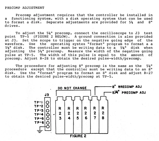
5~" READY OPTION JUMPER (JA-l)
While most 5~" drive manufacturers use "standard" pinouts for their drive cables, some drives have non-standard pinouts for features not found on all drives. In particular; MICROPOLIS, TEAC, and BASF drives use pin 6 for the READY output from the drive. MICROPOLIS and TEAC use pin 34 for the fourth DRIVE SELECT input. Other drives, such as QUME and the SHUGART SA410/SA460, use pin 34 for READY and pin 6 for the fourth DRIVE SELECT.
Jumper area JA-l (see sheet 1 of the jumper options drawings), in conjunction with JA-3 (below), reconfigures pins 6 and 34 of the 5~" drive connector J-l as required by the drives being used.
When 5~" drives without a READY output are used this option must be disabled as in Figure B. Figures C and D show the proper jumper settings for several drives that have a READY output.
5~" HEAD LOAD OPTION (JA-2)
MICROPOLIS and TEAC drives have a separate HEAD LOAD input on pin 2 of the drive cable. JA-2 (see sheet 1, figure E of the jumper options drawings) should be set according to either figure F or G depending on the drives being used.
5~" DRIVE SELECT #3 OPTION JUMPER (JA-3)
DRIVE SELECT OPTION (JA-4)
This option enables the drive select outputs of the controller either: whenever the MOTOR-ON line is active (drive motors are on), or only when the HEAD-LOAD output of the 1797 is active. In the drive select with motor-on position (see sheet 1, figure L of the jumper options drawings) the drive select outputs of the controller are enabled whenever the motors are on. This configuration is preferred when double headed drives are used, as it limits the number of times the heads are loaded and unloaded. In the drive select with head load position (see sheet 1, figure M of the jumper options drawings) the drive select outputs of the controller are only enabled when the HEAD-LOAD output of the 1797 is active. This configuration is preferred when using single headed drives.
SIDE SELECT OPTION JUMPER (JA-5)
This option allows the side select output, for double headed drives, to be controlled by either the side select output of the 1797 or by bit 6 in the boards DMA CONTROL REGISTER. This option is normally factory jumpered for side select from the DMA CONTROL REGISTER (see sheet 1, figure 0 of the jumper options drawings). This is the standard configuration for GIMIX 6809 FLEXm and other ~perating systems for this controller. If
a special application requires sioe select from the 1797, a trace must be cut and a solder jumper added to connect the pads as shown in sheet 1, figure P.
5\" and 8" PRECOMP OPTION JUMPER (JA-6)
[image:4.632.48.573.137.762.2]Drive manufacturers also specify a certain amount of precornp, usually between 100 and 400 ns. The board has provisions for separately adjusting the amount of precomp for 5~" and 8" drives. If the controller is purchased as part of a complete disk based system, the precomp is factory adjusted for the drives supplied. If purchased separately, the controller is adjusted to 150 ns. for 5~" drives and 175 ns. for 8" drives, or to the requirements of the drives being used, if specified when the controller was ordered.
The adjustments section explains the procedure for adjusting the board for the desired amount of precomp.
Consult the manufacturers literature to determine the precomp requirements of the drives being used.
8" MOTOR-ON DELAY OPTION JUMPER (JA-7)
Disk drives normally require a certain amount of delay for the motors to corne up to speed after they are started. This delay is provided by a timing circuit on the controller. If 8" drives that do not have motor control (the motors are always running) are used this delay can be eliminated. JA-7 (see sheet 1, figure Q of the jumper options drawings) enables or disables the motor-on delay as required. .
If 8" drives without motor control are used position the jumper as shown in figure R. If drives with motor control are used position the jumper as shown in figure S.
5~" HEAD-LOAD DELAY OPTION JUMPER (JA-8)
Most disk drives have a solenoid that loads and unloads the head(s). These drives r~quire a delay, after the heads are loaded, to allow time for the head(s) to settle. This delay is provided by a timing circuit on the controller. Some 5~",
double headed drives do not have a head load solenoid and the head is loaded as soon as the door is closed. These drives do not require any head load delay.
JA-8 (see sheet 2, figure A, of the jumper options drawings) allows the 5~" head-load delay to be disabled when drives without head-load solenoids are used, figure B, or enabled for drives with a head-load solenoid, figur~ C.
6800/6809 SLOW MEMORY SELECT OPTION JUMPER (JA-9)
SOFTWARE.WRITE PROTECT OPTION (JA-IO)
JA-IO (see sheet 2, figure G, of the jumper options drawings), in conjunction with bit 4 of the boards ORIVE SELECT REGISTER, allows the disk drives to be write protected under software control. When this option is enabled, figure H, and bit 4 of the DRIVE SELECT REGISTER is set low (0), all drives are write protected and no disk write operations are possible until bit 4 is set high (1). Since all bits in the DRIVE SELECT REGISTER are set low on system power up, bit 4 must be set high (1) after power up to enable disk writes. When this option is disabled, figure I, write protect is controlled only by the write protect signals from the individual drives.
JUMPER AREA (JA-Il) is reserved for future use.
BA/BS OPTION JUMPER (JA-l2)
DMA transfers to and from the board require a signal from the processor indicating that the bus is available to the controller. This signal is provided by the BUS AVAILABLE (BA) and BUS STATUS (BS) lines of the 6809 or the BUS AVAILABLE (SA) line of the 6800. JA-l2 (see sheet 2, figure M, of the jumper options drawings) is used to select either 6809, figure N, or 6800, figure 0, operation. JA-12 is factory jumpered for 6809 operation, figure N.
DMA OPTION JUMPER (JA-13)
The board is designed to use one of two different DMA methods, depending on which processor (6800 or 6809) is being used.JA-13 (see sheet 2, figure P, of the jumper options drawings) connects the Df.1A request signal from the board to either the BUSRQ line (6809) , figure Q, or to the HALT line (6800), figure R. JA"""13 is factory jumpered for 6809 DMA using the cycle steal method.
SLOW MEMORY OPTION JUMPER (JA-14)
Because of the timing requirements of the 1797, slow memory (MRDY) circuitry is required, at bus speeds above 1 MHz.,to stretch the system clock whenever the 1797 is acceased. JA-l4 (see sheet 2, figure S, of the jumper options drawings) connects the slow memory signal from the board to the proper bus line for the processor being used.
INTERRUPT OPTION JUMPER (JA-lS)
JA-lS (see sheet 2, figure X, of the jumper options drawings) is used to connect the interrupt output (INTRQ) from the 1797 to one of the interrupt lines of the bus. If interrupts are not used, jumper JA-lS as shown in figure Y • Figures Z, AA, and BB, show the proper jumper positions for generating interrupts on the NMI, FIRQ (6809 only), or IRQ lines respectively.
DIP-SWITCH OPTIONS
ADDRESSING OPTIONS (Sl and S2 sections 1 through 8) The board occupies 8 bytes of
board registers and 4 for the 1797 addressed to any 8 byte boundary in the address decoding (SS-SOC) is provided.
(Sl-l) enables or disables the extended board.
address space (4 for the registers) and can be address space. Extended DIP-switch Sl section 1 address decoding for the
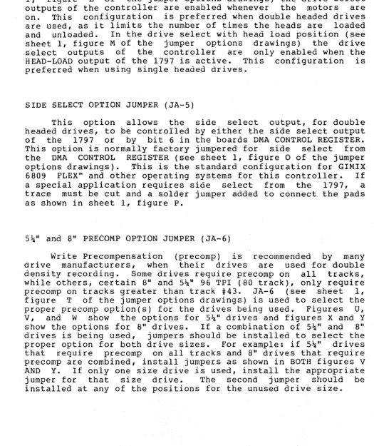
If Sl-l is OFF {OPEN} extended address decoding is disabled and the board only decodes the 16 regular address lines, AO through AlS. DIP-switch Sl sections 6 through 10 correspond to address lines A3 through A7 respectively. DIP-switch S2 sections 1 through 8 correspond to address lines AS through AlS respectively. These switches must be set to the desired base address of the board. A switch set ON (CLOSED) corresponds to a 1 (HIGH) on that address line and a switch set OFF (OPEN) corresponds to a 0 {LOW}.
If Sl-l is ON (CLOSED) the board decodes all 20 SS-SOC address lines, AO through A19 and, in addition to setting the base address of the board, Sl-2 through S must be set to the desired extended address. DIP-switch 51 sections 2 through S correspond to the extended address lines A16 through Al9 respectively. A switch set ON (CLOSED) corresponds to a I (HIGH) on that address line. A switch set OFF (OPEN) corresponds to 0
(LOW) '.
STANDARD GIMIX FLEX CONFIGURA'l'ION BOOTING ON A Sial! DRIVE
EXTENDED REGISTER BASE
ADDRESS ADDRESS
IE A A A A A A A A A
II
A A A A-A A AAI
511N
I
I II
3 4 5 6 78 9
I I I I I IA 6 7
8 9
51 52 0 I 2 3 4 50 0 0
00 0 0
0 0 0 ON= I0 0
0o
0
o
0 00
F F F F F F N N F N N N F F F N N N N
F F F F F F F OFF=£) F F F
E
N A
0 f
F
I 2 3 4 5 6 7
8 9 10
I 2 3 4 5 6 78 9 )0
L
EXT. ADDRESS DECODE FIG. t5" OR 8" BOOT
SELECT~
[image:7.630.52.596.248.771.2]5~" or 8" SENSE SWITCH (S2 section 9)
Bit 0 of the DRIVE SELECT REGISTER is provided to allow the size (5~n or 8") of the drive installed as drive 0 to be determined by software. The status of this bit is determined by setting 82-9. If drive 0 is a 5~" drive, S~-9 should be set ON
(CLOSED). If drive
6
is an 8" drive, set S2-9 OFF (OPEN). \l~MA EXTENDED ADDRESS OPTION .(S2 section 10)
The board is capable of driving the SS-50C extended address lines, A16 through A19, during DMA transfers. This allows the board to perform DMA transfers to and from any address in the 1M byte address space of the SS-50C bus. If S2-10 is OFF (OPEN) this option is disabled and the controller only drives the 16 regular address lines AO through A15. If S2-l0 is ON (CLOSED) the controller drives all 20 address lines of the S-50C bus.
The address presented on the 4 extended address lines is
determined by the data stored in the lower 4 bits of the DMA CONTROL REGISTER. Bits 0 through 3 of the DMA CONTROL REGISTER
correspond to extended address lines A16 through A19
respectively.
BOARD REGISTERS
The to any extended of the standard
board occupies
a
memory locations and can be addressed 8 byte boundary in the address space ( 1M BYTE with addressing). The following table lists .the functions8
10catiOtiS and assumes that the board is set to the GIMIX FLEXm address, $E3BO.Base address $E3BO
$E3Bl $E3B2 $E3B3
Drive Select Register DMA Status Register DMA Control Register DMA Starting Address DMA Starting Address
(write}
Base address +7
$E3B4 $E3B5 $E3B6 $E3B7
( read)
(write only) (MSB)
(LSB)
1797 Command/Status register 1797 Track Register
1797 Sector Register 1797 Data Register
The four 1797 registers are internal registers in the 1797 floppy disk controller
I.e.
Information on their functions and programming c.an be found in the manufacturers data sheets for the 1797 •.NOTE: Accessing any of the 1797 registers starts the drive
motors.
The first four registers control various functions as
MSB
LSB
DRIVE SELECT REGISTER ($E380 Write only)
BIT
7
BIT 6
BIT 5
BIT 4
BIT 3
BIT 2
BIT 1
BIT 0
RESERVED
CONNECTOR SELECT
o
=
SJ..i"
I
=
8"DENSITY SELECT
o
=
Double den. 1=
Single den.WRITE PROTECT
o
=
W/protect I=
W/enableDRIVE SEL. 3
DRIVE SEL. 2
DRIVE SEL. I
DRIVE SEL. 0
Reserved for future use.
Selects between the
5J..i"
and8"
drive connectors. Also selects the proper data separator rate and precomp.
Selects between single and dou-ble density operation. Selects proper data separator rate and enables precomp for· double den.
Write protects all drives when enabled. SOFTWARE WRITE PROTECT OPTION JA-IO must be enabled to use this feature.
Bits 0 through 3 perform a 1 of 4 drive select function. Any bit set to a 1 selects
the associated drive. Only one of the four drives select bits should be a 1 to prevent multiple drives from being selected.
0
=
drive selected I=
drive deselectedLSB
BIT 7
BIT 6
BIT 5
BIT 4
BIT 3
DMA STATUS REGISTER
DRQ FLAG
INTRQ FLAG
o
=
No INTRQ1
=
INTRQMOTOR DELAY FLAG
o
=
Running 1=
StartingDMA ENABLED FLAG
o
=
DMA Disabled 1=
DMA EnabledDMA FAULT FLAG
o
=
NO DMA FAULT 1=
DMA FAULT($E380 Read only)
This bit is the same as the DRQ bit in the 1797 status register and the output of the 1797 DRQ signal. See the 1797 data sheet.
Indicates the state of the INTRQ interrupt output from the 1797. This bit is set to a 1 when an
interrupt is generated an cleared to 0 when the 1797 status register is read. Active even when bus
interrupts are disabled.
Indicates that the drive motors were stopped then restarted. Used to eliminate software timing when checking for "drives ready".
Indicates that DMA transfers are enabled and an occurence of the 1797 DRQ will cause data to be transfered between the board and memory.
Indicates that a DMA transfer longer than 16,384 + or - 256 bytes was attempted and the board has stopped the transfer. This can occur because of a hardware fault or if a drive door is opened during a track write (formatting).
NOTE: Data must be written to the DMA STARTING ADDRESS REGISTER (LSB) _ to reset the DMA FAULT counter and prevent false DMA FAULTS from occuring.
BIT 2
BIT 1
BIT 0
CONNECTOR SELECT FLAG
o
= 5la"1 = 8"
RESERVED
SENSE SWITCH FLAG
1
=
S2-9 OFF (8")o
= S2-9 ON (5la")Indicates the drive size, 5\" or 8", turrent1y selected by the CONNECTOR SELECT bit in the DRIVE SELECT REGISTER.
Reserved for future use
Indicates the state of the sense switch, S2-9. Used by GIMIX FLEX~
L&B
LSB
DMA CONTROL REGISTER ($E3Bl
BIT 7
BIT 6
BIT 5
BIT 4
BIT 3
BIT 2
BIT 1
BIT 0
INTERRUPT ENABLE
o
=
Int. Disable 1=
Int. EnableSIDE SELECT
o -
Side Zero1
=
Side OneDMA DIRECTION
o
=
READ FROM DISK 1=
WRITE TO DISKDMA ENABLE
o
=
DMA DISABLED I=
DMA ENABLEDAl9
AlB
Al7
A16
~'iRITE ONLY)
Enables the interrupt output from the board to the bus. Interrupt jumper JA-15 must also be set for the desired interupt line. Allows software switch between interrupt and non-interrupt operation.
Used to select between side zero and side one when using double-headed drives. Side select jumper JA-5 must be set for side select from control register in order to use this bit.
Sets the direction for DMA
transfers between disk and memory.
Enables the DMA circuitry for
transfers between disk and memory. DMA must be enabled before a read or write data command is issued to the 1797.
DMA STARTING ADDRESS REGISTERS ($E3B2 and $E3B3 WRITE ONLY) The source/destination address for a DMA transfer must be written to the DMA STARTING ADDRESS REGISTERS before a transfer is initiated by issuing a read or write command to the 1797. After each byte is transfered the address is automatically incremented arid another byte is transfered, until the 1797 read or write operation is complete. The most significant byte of the 16 bit address is stored in the MSB register ($E3B2) and the least significant byte in the LSB register ($E3B3). If extended addressing (20 bit) is used the extended address is written to the DMA CONTROL REGISTER bits 0 through 3 (see above). Since the extended address cannot be changed while a DMA transfer is in progress, a single transfer cannot be made to or from more than one bank.
Writing to the DMA STARTING ADDRESS REGISTER (LSB) resets the DMA FAULT counter. This register must be rewritten before every DMA transfer to a false DMA FAULT from occuring.
PROGRAMMING FOR THE GIMIX DMA CONTROLLER This section is included as
board, for the user who wishes to or adapt the board to an existing on programming the 1797 can be literature. .
DRIVE SELECT REGISTER (WRITE)
a guide to the features of the write his own operating system operating system. Information found in the manufacturers
The functions of the DRIVE SELECT REGISTER bits are described in the preceeding section. On power up or after a system reset the following conditions exist:
5%"
drives, double density, and write protect of all drives is selected. All drives are deselected. Before a disk transfer is initiated the drive size, density, and write prot~ct should be set as required and one of the drives selected by setting the appropriate drive select bit to a fll".DRIVE SELECT REGISTER Reading the DRIVE various functions of flags are described i~ information on those below.
(READ)
SELECT REGISTER indicates the status of the board. The basic functions of the the·preceeding section~ More detailed that have special significance is given
BIT 7: The DRQ flag is not normally used for DMA transfers, it is only required if the board is used as a programmed I/O controller.
BIT 5: The MOTOR DELAY FLAG can be used in routines that check for "drives ready". Normally these routines must include a delay loop to insure that a "drives not ready" condition is not caUsed because the drive motors are not yet up to speed. The MOTOR DELAY FLAG eliminates the need for delay loops which make the software dependant on system clock speed. To use the MOTOR DELAY FLAG, first check the "drives ready" status from the 1797. If this indicates that the drives are ready, normal operation can proceed. If the drives are not ready, the MOTOR DELAY FLAG should be checked. If the MOTOR DELAY FLAG is LOW (O), the motors are at speed and the "drives not ready" can be considered valid and proper action taken to handle the error. If the MOTOR DELAY FLAG is HIGH (1), it should be rechecked until it goes LOW (0). The HIGH to LOW transition indicates that the drive motors have been on long enough to corne up to speed. The "drives ready" status from the 1797 should again be checked and if it still indicates "drives not ready" the condition can be considered valid (no disk in the selected drive, door open, etc.) and proper action taken to handle the error. If it indicates that the drives are ready, normal operation can proceed.
BIT 3: Because the 1797 track read and track write commands read or w~ite data continuously, starting when one index pulse is received from the drive and ending on the next, it is possible for control of a transfer to be lost because of a hardware failure or because the drive door' is opened during a track write. If this were to occur the board would cycle continuously through the entire address range reading from memory. This runaway condition is prevented by a counter which limits the maximum transfer to 16,384 + or - 256 bytes. If the maximum count is reached the transfer is halted and the DMA FAULT FLAG is set HIGH (1) to indicate a DMA FAULT. The DMA FAULT FLAG should be checked at the completion of any 1797 track write commands to determine if a DMA FAULT has occurred. The DMA FAULT COUNTER is reset by writing to the DMA STARTING ADDRESS REGISTER (LSB). Data must be written to this register before each DMA transfer to reset the counter and prevent false DMA FAULTS.
DMA CONTROL REGISTER
The functions of the DMA CONTROL REGISTER are described in the preceeding section. More detailed information for some of the bits is given below. On power up or after a system reset all bits are cleared to 0; interrupts are disabled, side 0 and read are selected, DMA is disabled, the extended address is set to $0. These
DMA STARTING ADDRESS REGISTERS (MSS and LSS)
The source or destnation address for a DMA transfer must be written to these registers before the transfer is initiated. Once the transfer is started the board increments this address each time a byte is transfered. At the completion of a transfer
the DMA STARTING ADDRESS REGISTERS point to the address
following the last byte transfered. It is not necessary to
write a new value to the MSB register if a second transfer is to be made, continuing from this address. The LSB register should be re-written, before each transfer or before 16,128 (16K-256) bytes have been transfered, to reset the DMA FAULT counter. IF THE DMA FAULT COUNTER IS NOT RESET BEFORE MORE THAN 16,128 BYTES
ARE TRANSFERED A FALSE DMA FAULT WILL OCCUR, HALTING DMA
TRANSFER.
HEAD LOAD DELAY
The board has two separate delay circuits, one for 5~"
drives and another for 8". The proper circuit is selected by the CONNECTOR SELECT BIT. These delays are used to provide the required settling time, after the heads have been loaded. The delay starts whenever the head load output from the 1797 (HLD) becomes active (HIGH). After the delay, the head load timing input to the 1797 (HLT) is made high indicating to the 1797 that thee heads are loaded and have had time to settle. The HLT input is also controlled by another delay circuit that provides a delay for the drive motors to come up to speed. Both the HEAD LOAD DELAY and the MOTOR-ON delay must be completed before the HLD input is made HIGH.
Once the HLD output is made active (HIGH), by issuing a command to the 1797 that loads the heads, it does not become inactive (LOW) again until it is specifically reset by issuing a command that unloads the heads or until 15 revolutions of the disk have occurred since the 1797 completed its last command.
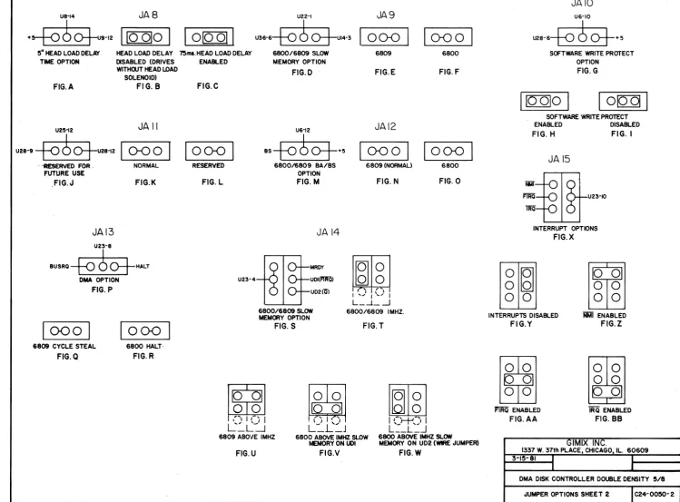
ADJUSTMENTS
There are six trimmer potentiometers, located at the top of the,
board,
that are
used to adjust the data separator and the precomp
circuits. The data separator is factory
adjusted
and
should
not
require readjustment unless the trimmers are moved accidentally or a
component in the data separator circuitry is replaced.
The
precomp
circuits may
require adjustment
to suit the drives being used or
when changing
from one
type
of drive to
another.
The
drive
manufacturers
literature should be checked to determine the precomp
requirements of a particular drive.
The
data separator adjustments are factory set and should not
be changed.
If the data separator
requires
readjustment please
contact the facotory for information.
The following paragraphs describe the proceedure for
adjusting
the precomp circuits for both
5~"and 8" drives.
These adjustments
require an oscilloscope with an
accurately calibrated time
base.
Unless
preformed
with care
and the proper test equipment, making
these adjustments can cause more harm than good.
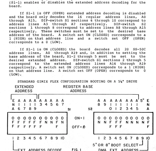
PRECOMP ADJUSTMENT
Precomp adjustment requires that the controller be installed in
a
functioning system, with a disk operating system that can be used
to format a disk.
Separate adjustments are provided for
5~and
8"
drives.
To adjust the
5~"precomp, connect the oscilloscope to J3
test
point TP-5
(FIGURE 2 BELOW).
A ground connection is also provided
at J3.
Set the scope to trigger on the negative going edge of
the
waveform.
Use
the operating systes "format" program to format a a
5~"
disk.
The controller must be writing data to a
5~"disk when
adjusting
the
5~"precomp.
Measure the width of the negative going
pulse at TP-S.
The width of this pulse is equal to
the amount
of
precomp. Adjust R-28 to obtain the desired pulse-width/precomp.
The proceedure for adjusting 8"precomp is the same as the
5~"proceedure
except that the controller must be writing data to an 8"
disk.
Use the "format" program to format an 8" disk and adjust R-27
to obtain the desired pulse-width/precomp at TP-5.
DO NOT CHANGE
r -
S" ftRECOMP ADJI
. I
I
I
!S~"
'PRECOMP ADJJ3
TP-I
0
TP-2
0
R
R
R
R
R
R
TP-3
0
TP-4
0
~2
2
2
2
2
2
TP-f)
0
3
4
,~6
7
8
TP-6
0
[image:15.630.45.590.285.769.2]6800 OPERATION BOARD CONFIGURATION
The controller designed to work in both 6809 and 6800 systems. As delivered the boards are configured for 6809 operation and several jumpers must be change to configure the board for 6800 systems. In most cases the jumpers for 6809 operation consist of PC board traces or solder jumpers connecting the pads indicated in the jumper configuration drawings. To reconfigure the board for 6800 systems the PC board traces must be cut or the solder jumpers removed and new jumpers installed to connect the pads indicated for 6800 use. The following jumper areas must be changed for 6800 operation: JA-12 and JA-13. If the board is to be used in 6800 systems running above I MHz. jumper area JA-9 must also be changed and JA-14 configured for the proper 6800 slow memory option (see the following section). In I MHz. 6800 systems the SLOW MEMORY OPTION jumper JA-14 should be configured as shown in figure T.
6800 SLOW MEMORY
Operation in 6800 systems above I MHz. requires that the CPU board have provisions for a MEMORY READY (MR) input on either UD-I or UD-2. MEMORY READY is available on the GIMIX 6800 CPU BOARD as a jumper option. To enable the MR option on the GIMIX 6800 CPU BOARD connect a wire jumper from the pad labeled "MR" (there is a mistake in the drawing included with the board, use the corrected drawing below) to the desired user defined line; either UD-I or UD-2. Jumper area JA-14 on the disk controller should be set to match the UD line chosen on the CPU. No other modification to the system is required.
G
GR
o
RG
D
MEMORY
READY
MR
Q
/
,
/
,
DR
D
o
UD20
UD IGIMIX 6800 CPU MEMORY READY JUMPER FIGURE 3
The SWTPc MPA-2 6800 CPU board requires minor hardware modifications to provide the MEMORY READY input. To modify the MPA-2 for use with the controller above I MHz.: cut the small trace, on the solder side, connecting pin 6 of IC 6 (the 6875) to the large trace running between the pins of IC 6. This disconnects pin 6 of the 6875 from the +5V supply. Connect a jumper from IC 6, pin 6 to the desired user defined line: UD-I or UD-2. Finally connect a 4.7K ohm resistor from IC 6, pin 6 to the +5V supply. This completes the MPA-2modifications. JA-14 on the disk controller board should be set to match the UD line chosen on the CPU. No other modification
DISK DRIVE CONFIGURATION DRIVE CONNECTIONS
Standard 34 pin (Jl) and 50 pin (J2) connectors are provided for the 5~" and 8" drive cables respectively. The proper connector is selected automatically when the controller is switched between 5!:i" and 8" drives using the CONNECTOR SELECT bit in the DRIVE SELECT REGISTER. The length of the cables between the controller and the drives should be to a minimun to.reduce noise pickup. Ten feet should be considered an absolute maximum for the length of the drive cables.
DRIVE PROGRAMMING
Any combination of 5!:i" and 8" drives, up to four drives total, can be connected to the controller. The drives themselves must be programmed to respond to the desired drive number (drive select 0, 1, 2, or 3). See the drive manufacturers documentation for infromation on programming specific drives. If only one size drive is used the drives should be programmed in sequence starting with drive O. If both5!:i" and 8" drives are used they can be arranged in any desired order starting with drive O. For example: if two 5!:i" and two 8" drives are used, the 5!:i" drives could be programmed as drives 0 and 1, the 8" drives would then be 2 and 3~ If the 8" drives were programmed as . drives 0 and 1, the 5!:i" would then be progammed as 2 and 3. They could also be arranged so that drives 0 and 2 are 8" and drives 1 and 3 ar~ 5~" etc. Regardless of the order chosen, the 5~" or 8" SENSE SWITCH (S2 section 9) must be set to match the size of the drive programmed as drive O.
DRIVE TERMINATION
In order for the controller to function properly, the drive cables must be properly terminated. Ter~inating resistors are provided on the disk drives to terminate the cables. When more than one drive is connected to a single cable the terminating resistors on all drives EXCEPT the last one on that cable (the drive farthest from the controller) must have their terminating resistors removed or disabled. Only the last drive on the cable should have a terminator. If both 5\" and 8" drives are used the last drive on both cables must have a terminator. Consult the drive manufacturers documentation for information on removing or disabling the terminators.
-15-UI-4 '1
0-00
~1-6-
r-o
?
0-~~1-34
5" READY OPTIONS FIG.A
U3-11
~1-34-f""O
c5
0"t~1-6
S' DRIVE SELECT *3 OPTION
FIG. H
U4-11
U29- 9
-f"O
c5
O"t
U26-11SIDE SELECT OPTION FIG. N
JA I
loo~
000
READY DISABLEDFIG.S
JA3
10lQQJI
NORMAL FOR MOST DRIVES SHUGART, MPI,SIEMENS,ETC.
FIG.I
JA5
10001
SIDE SELECT USING CONTROL REGISTERFIG.O
I
o~o
000
I
READY FROM PIN 34 QUME, SA41O/SA460
ETC. FIG.C
110010
I
TEAC/MICROPOLIS
FIG.J
I
OOD
I
SIDE SELECT USING 1797 OUTPUT
FIG. P
JA6
0-000-6
QQQQQ
00000
00'000
00000
-00000
t§0o
I
000
READY FROM PIN 6 TEAC/MICROPOLIS
FIG.D
00000
00000
uzt-l
I .... 5" PRECOMP DISABLED 5"PRECOMP ON ALL TRACKS 5"PRECOMP ABOVE TRACK 43( 80 TRACK DRIVES) 5"88" PRECOMP OPTIONFIG.T FIG.U FIG.V FIG.W
JA2
~1-Z-fO
OO+-UZ-III
000
I
I
[QQlo
I
5" HEAD LOAD HEAD LOAD DISABLED HEAD LOAD ENABLED TEAC/MICROPOLIS
FIG. E FIG.F FIG. G
U3-Z
UI-1Z-f""O
~
O"tUZ-SDRIVE SELECT OPTION
FIG. K
"'-'-to
6'03-"
8" MOTOR ON DELAY OPTION
FIG.Q
JA4
1
Killo
I I
O[QQ]
I
DRIVE SELECT WITH DRIVE SELECT WITHMOTOR ON HEAD LOAD FIG. L FIG.M
JA7
10[QQ}1
1[QQ]0 I
NO MOTOR-ON DELAY ISEC MOTOR-ON DELAY (DRIVE MOTORS ALWAYS
ON)
FIG. R FIG. S
00000
oooog
00000
8"PRECOMP ENABLEDABOVE TRACK 43
-ooogo
FIG.Y8"PRECOMP DISABLED
GIMIX INC.
1337 W. 37th PLACE CHICAGO IL. 60609
US-14
JA8
+~3O+9-'2
110010
I
SOl HEAD LOAD DELAY HEAD LOAD DELAY TIME OPTION DISABLED (DRIVES WITHOUT HEAD LOAD
SOLENOID)
FIG. A FIG.B
U25-12
JA II
U2S-9-i"'O
25
OJ-U28-12I
000
I
--'iESERVEO FOR . NORMAL FUTURE USE
FIG.J FIG.K
JAI3
U23-S
BUSRQ
-fO
<5
ot-
HALTDMA OPTION
FIG.P
1000
I
6809 CYCLE STEAL
FIG.Q
1000
I
6800 HALT·
FIG.R
U22-1
JA9
1010011
U36-6-fO 3 O+U14-3I
000
I
I
~ml. HEAD LOAD DELAY 6800/6809 SLOW
I
ENABLED
FIG.C
000
I
RESERVED
FIG.L
MEMORY OPTION
FIG.D
U6-12
S S - f O
25
03-+
5680016809 BAIBS OPTION
FIG.M
JAI4
m
MRDYU23-4 UDlIJ!mQl
UD2~ 6800/6809 SLOW MEMORY OPTION
FIG. S
I~;~!
L-=-L~
Ilg!gll
L:....L~J
6809
FIG.E
JAI2
I
000
I
I
6809 (NORMAL)
FIG.N
I~I~I
I ... I ' .... '" I
L_ .... ,L..J
6800/6809 IMHZ.
FIG.T
1[g]lg I
I'-~-~J I L~_L~J000
I
6800
FIG.F
000
I
6800
FIG. 0
6809 ABOVE IMHZ 6800 ABOVE IMHZ SLOW MEMORY ON UDI
6800 ABOVE IMHZ SLOW MEMORY ON UD2 (WIRE JUMPER)
FIG.U FIG.V FIG.W
JAIO
U6-IO
U2S-6-f{)
c5
0++
5SOFTWARE WRITE PROTECT OPTION
FIG.G
11QQ]0
I
10~1
SOFTWARE WRITE PROTECT ENABLED DISABLED
FIG. H FIG. I
JAI5
F:~U23-IO
~~
INTERRUPT OPTIONS
FIG.X
Igijl
rn
INTERRUPTS DISABLED
FIG.Y
~
~
FIRQ ENABLED
FIG.AA
g
o
o
0
o
0
R ENABLEDFIG.Z
~
~
IRQ ENABLEDFIG.BB
.~~MIX INC.
1337 W. 37th PLACE, CHICAGO IL. 60609 3-IS-81 I
I I
[image:19.791.14.764.13.566.2]+8<--1 U49 +5A
S-l
+ +
-'-C43 C41 -'-- 1...-,
-,..- -.-- _.--C20-C25
*
U50 +59
+
-'-C44 C35 - ' - --C27-C42
-,..- '-,..-
--'
"
-:l
-+16< ,- U51 +12
+ +
-'-C34 C33 - - --C26
--,- --.-- -,..-'
GNoD
1-PONER 8 GROUND PINOUTS
IC. NO. +5A +59 GND.
NOTE: UI9 PIN I UI 20 10
CONNECTED TO +12 U2 14 7
U3 14 7 U4 14 7 U5 14 7 U6 14 7 U7 14 7 U8 16 8 U9 16 8 UIO 14 7 UII 14 7 UI2 14 7 UI3 16 8 UI4 14 7
TEST JACK UI5 UI6 14 18 7 9
J3 UI7 20 10
UI8 15816 889 UI9 21 20
8=
'-TPI U20 U21 16 16 8 8 -TP2 U22 U23 16 14 8 78=
-TP3 U24 U25 14 14 7 7U26 16 8
-TP4 U27 16 8
0-
-TP5 U28 U29 20 20 10 10?
-TP6 U30 U31 16 16 8 8U32 16 8 U33 16 8 U34 20 10
-L
U35 20 JO- U36 14 7
U37 14 7 U38 16 8 u39 14 7 U40 14 7 U41 14 7 U42 14 7 U43 14 7 U44 14 7 U45 20 10 U46 20 10 U47 20 10 U48 20 10
,S?IMIX INC.
1337 W. 37th PLACE. CHICAGo..IL. 60609 3-17- 81
l
DMA DISK CONTROLLER I LOGIC SUPPLY PROPRIETARY MAT'L., ALL RIGHTS
RESERVED @Isel GIMIX INC.
I
L24-~0-1I
M
,...
<:t
o
BOOT FOR GIMIX DMA CONTROLLER 5-12-81 GIMIX, INC PAGE 1 E3BO E3BO E3B1 E3B2 E3B4 E3B6 E3B7 F806 F810 F812 FOOO
FOOO 10CE DFFF
F004 34 F006 86 F008 lF FOOA 86 FOOC 97 FOOE 86 F010 97
08 E3 8B DO B4 01 B6 ********************************************
*
*
*
*
*
*
*
*
*
*
*
*
*
*
*
*
*
*
GIMIX 6809 RELOCATABLE DISK BOOT
*
*
FOR GIMIX DMA DISK CONTROLLER
VERSION 3.2
Michael H. Katz
Copyright (C) 1980 by GIMIX, Inc.
1337 West 37th Place Chicago, Illinois 60626 (312) 927-5510
All rights reserved
*
*
*
*
*
*
*
*
*
*
*
*
*
*
*********************************************
*
EQUATES FOR DISK BOARD*
PORT EQU $E3BO
DRVREG EQU PORT DMAREG EQU PORT+1 ADDREG EQU PORT+2 COMREG EQU PORT+4 SECREG EQU PORT+6 DATREG EQU PORT+7
*
*
GMXBUG-09 ENTRY POINTS*
INCHE EQU $F806 PSTRNG EQU $F810
LRA EQU $F812
*
ORG $FOOO
*
*
START OF DISK BOOT*
BOOT
*
LDS II$DFFF
BASE ADDRESS OF CONTROLLER
CONTROLLER DRIVE SELECT REGISTER DMA CONTROL REGISTER
DMA ADDRESS REGISTER
1797 COMMAND/STATUS REGISTER 1797 SECTOR REGISTER
1797 DATA REGISTER
INPUTW/ECHO PRINT STRING LOAD REAL ADDRESS
MOVE STACK
*
DELAY TILL MOTORS UP TO SPEED.*
DELAYS UNTIL THE MOTOR DELAY BIT*
GOES LOW OR WHEN DRIVE BECOMES READY.*
PSHS LDA TFR LDA STA LDA STA DP II$E3 A,DP fl$DO <COMREG 1f1 (SECREGPRESERVE DP REGISTER BASE PAGE OF CONTROLLER SET DP-REG.
CODE FOR CLEAR INTERRUPT GIVE IT TO FDC
BOOT FOR GIMIX DMA CONTROLLER 5-12-81 GIMIX, INC PAGE 2
F012 97 F014 D6 F016 2A F018 D6 F01A C5 F01C 26 F01E 86 F020 D6 F022 54 F023 24 F025 8A F027 97 F029 86 F02B OF F02D C6 F02F 8D F031 4A F032 26 F034 C6
F036 4F F037 8D F039 C5 F03B 27 F03D 8E F040 AD F044 9F F046 8A F048 C6
F04A 8D F04C C5 F04E 26 F050 35 F052 7E
F055 58 F056 24 F058 30 F05C AD F060 30 FQ64 AD F068 AD F06C 84 F06E 81 F070 27 F072 81 F074 26 F076 6E
BO
B4 BOOTl
06 BO 20 F6
21 BOOT2
BO
02
CO EIGHT
BO DRVOUT
03 Bl
5B LOOP
4D F9 DB 43 04 18 COOO 9F F812 B2 10
BC
30 9C 05 08 COOO*
*
*
STA LDB BPL LDB BITB BNE LDA LDB LSRB BCC ORA STA LDA CLR LDB BSR DECA BNE LDB CLRA BSR BITB BEQ LDX JSR STX ORA LDB BSR BITB BNE PULS JMP <DRVREG <COM REG BOOT2 <DRVREG 11$20 BOOTl 11$21 <DRVREG DRVOUT II$CO <DRVREG 113 <DMAREG 11$5B CHKRDA LOOP II$OB CHKRDY 1104 ERROR II$COOO [LRA] <ADDREG 11$10 11$8C CHKRDY f/$9C ERROR DP $COOOGIVE TO CONTROLLER GET STATUS FROM 1797 LOOP IF NOT READY GET STATUS
MOTOR STARTING UP?
YES: WAIT FOR BIT TO GO AWAY
SETUP BITS FOR DRIVE SELECT REGISTER GET DMA STATUS
EIGHT INCH DRIVE? NO: CONTINUE
SELECT 8", SINGLE DENS & DRIVE 0 SELECT DRIVE
NUMBER OF TRACKS TO STEP IN DISABLE DMA
STEP IN WITH UPDATE WAIT FOR READY DECREMENT COUNTER LOOP TILL DONE
HOME AT 40ms PER STEPPING PULSE, LOAD HEAD AND VERIFY POSITION DISABLE DMA
GIVE COMMAND
&
WAIT FOR READYCHEC~ FOR TRACK ZERO
IF NOT THEN ERROR
ADDRESS TO LOAD FROM DISK GET REAL ADDRESS
GIVE ADDRESS TO CONTROLLER SET DMA ENABLE
READ SINGLE RECORD, IBM FORMAT, HLD, HLT AND 10 ms DELAY
EXECUTE AND WAIT TILL DONE ANY ERRORS?
YES: PRINT ERROR MESSAGE RESTORE DP REGISTER
NO: FINISHED, JUMP TO NEXT BOOT
*
ERROR ROUTINE08 8D 0044 9F F810
*
CHECKS FOR DRIVES NOT READY*
AND TELLS THE USER IF THAT IS*
THE CASE.*
ERROR NOT READY?ERRORl NO: PRINT NORMAL MESSAGE NRDYMS,PCR POINT TO MESSAGE
[PSTRNG] PRINT IT 8D 0024 ERROR1
9F F810
ASLB BCC LEAX JSR LEAX JSR JSR ANDA CHPA BEQ Cl1PA BNE JI1P
ERRMSG,PCR POINT TO ERROR MESSAGE [PSTRNG] PRINT IT
9F F806 5F 59 8E 4E EA 9F FFFE
[INCHE] WAIT FOR CHARACTER f/$5F MAKE UPPER CASE "Y IS IT A 'Y'? BOOT YES: TRY AGAIN
lit N
ERRORl [$FFFE]
IS IT AN 'N'?
BOOT FOR GIMIX DMA CONTROLLER 5-12-81 GIMIX, INC PAGE 3
*
HARDWARE RESET VECTORF07A 20 E4 BRA ERROR1 PRINT ERROR MESSAGE AND GOTO RE-TRY
F07C 97 F07E D7 F080 D6 F082 58 F083 2A F085 D6 F087 39
B1 B4 BO
FB B4
F088 45 52 52 4F F09F 04
FOAO 4E 4F 54 20 FOA9 04
o ERROR(S) DETECTED
*
*
THIS ROUTINE WAITS FOR THE*
FDG TO FINISH EXECUTING*
THE CURRENT COMMAND.*
CHKRDY STACHKRDA STB CHKRD1 LDB
*
ASLB BPL LDB RTS
<DMAREG <COMREG <DRVREG
CHKRD1 <COMREG
GIVE TO CONTROLLER GIVE TO 1797
GET STATUS FROM 1797 DONE?
NO: WAIT TILL DONE RETURN STATUS IN B
*
ERROR MESSAGES*
ERRMSG FCCFCB NRDYMS FCC ·FCB END
IERROR IN BOOT, RE-TRY? I
$04
INOT READYI $04
BOOT
BOOT FOR GIMIX DMA CONTROLLER 5-12-81 GIMIX, INC PAGE
SYMBOL TABLE:
ADDREG E3B2 CHKRDA F07E DRVOUT F027 ERROR1 F060 PORT E3BO
BOOT FOOO CHKRDY F07C DRVREG E3BO INCHE F806 PSTRNG F810
BOOT1 F014 COMREG E3B4 EIGHT F025 LOOP F02D SECREG E3B6
BOOT2 F01E DATREG E3B7 ERRMSG F088 LRA F812
CHKRD1 F080 m1AREG E3B1 ERROR F055 NRDYMS FOAO
A'S '>---.--+~--""~'-\U39 4 '
AI)
~A2>>---d--+~I~~U39 II At
-[,0'
~ U41
+5
VMA ....
>----+---'~"l
I , PUAJRP2-~
A3<" Iz1U411" , ,
r
Is
PlPlI-h ~D
I r - - I l ~
. ::: <.<.>--~--"-l5U 4 4 . 1
Al4 • 10
AI5
<. 1% 13 3.U.11~6~~~~~~~~~~~~~~~"--~i
~
3
.>o-"-=-2----++-tuse
=
I
I _UII~~BI~JA7 '~r-
S1l
lt
A8 • +5~ 5 ~Y2 14 I.--USI T 6 U7 1,- PUA
e I5SW 15~ I w UIO ,.,9'--_-H, A2r'--' I[ I~ R'
L-'-: CLR CLKf=--- 12, m~
--v::=
...! Y4 8 10 • 10 9 5 Q A ~RIO
C8
14C[H,5
13 Q A-L,
U. -"!,,.
I RPI-D
~4;;S
~
JI J2
a 20
-6-~ TNDEX
+5
use
I I~
2~
~ ~7 :I~ :~
I
I~~
2 r ! _ ---L Y3 : : PUAfflf'
10~
1<; sclf::j 7PUA~ T U P 7 ~ • r--~2 A • .!.4-ooooc U. ' -"!,,.
~~U4~~ QA LOfL---'="""-+++++, IC5 Gle!. fP~ 15= I I )000<; IJ~6 uz 12", 10 4
e1-~ '-~Qa50 A~
=
'
9--=,
w ail L-.:.Q ,~ '8 "QC a~' ~ 6 UI f>l!J. 5 Aa UI9 'WJIIn'~ PUA\-W 10 UI4 S CLR CLR RPI-E
/~ ~ QO C~ 7
L-.!!!1
,¥--
S AI ' -Irl-'
S '"""1M"'" '---'~ , . ~1-'-"5,--+-+--{~ --.J\ WPROTECT- -
~~
~
'2.~~~~~~
TRM~
1r~===~~~bd---'=~~c=~ff=¥~~~~~~~~~~~~=~1Hl~ue~ul'-l
~~
~U46H~~
lU:6'~ lIuI0.:~~9 ~D2' ~:; .:::'~
n
h
H:G-:::u><a,r'32'--<1'--:-'C:~-i·V
...
~
".1':
~ • 12 O~ ..
rI
~ OALa >~ ~~, 12 +6--"""'<~. , 1-'-'-7-+--+-{O---O TRACK ~~-OJ:~~;
=
~
j
.:,:~- ~/ ~'>~ ~\'::_=_=r:=::=========::===U~:;25~_=_=_=1\--' R~~2 ~2Q'2 ~22Q3
::>22::
\~'
"U~4 12~
-0
934 DIRr-~~---+---' ~
TG-43r29"---+---'~
R45 11]~,",
...~CLA
i Z.I." / , ~~-'Vv\',-"-fl U 16 RI4 " 111'2
""lTCLKp2~---t~ ~ II I .>o--'-"-_+--t_--' I 7 ~ OAL7 HLO ~2I,--_+-_ _ _" . II 3 5 7 I
rcl.
Z' 4 20 H1,It ~CLR Pt'----+f-t-H / ~' I,' '- • e __ 3 • ;::;. 9~ I ~ -'--II I. QA U LO'-':--lLl»"""H+H-H---"1 3 3 " UI- - ~ -\..J
"'I;.r-VA. I U45 13 13 51 r3 oa .--_ _ _ _ _ _ _ 3"-7'-l1Xmi ~p"-.---+---, 12 UI4 "~TPe "':!-,,, 115 US
v.:::----:-
r---QI A~ 19 19 3 2 4 R20 'L 9-[::?';- =' 3 .>o~4L-t_-_+----'~ 15 12 C I~ r---"'-IIIR WG 30 04 Il'! ~ 01 ~5 . A A I > - -
r---"-i
I ~ 17 II 0 ~5 02 ,---~~7':l4 ~ 1 9 e I>--__.o-+---''----J IO 9 U I
A.=,.,..,..,.... ..
c= V ' - - - - 15 AC O. r---=_ICLK Y---=-ITG-43 STI- r-I &IJ'~.I
-pf.-
y - - - < - f ;><l~-___jl_-+_-I_VJ TRACK 44.76~ -~ ff20 OND WOt-='''---t--, ' - - + - - - _ - 18'iFOl PU 13 J._:: QI '---"', 4· I ~A,'O
~ '--_+--.---_ _ _ -'-\7 WG Jilj ~ r- PUA 5 • 8""10--'6'----+---+----,
12 ~ 3 04 ~ 3 ~ 7 S ! ! " J
AI2 3 - fl' 14 A U a ~ II 12 - 25 SSO E 1--"-' - - + , '----+-+---'-1' WO WOOUT ~, RI9 2 3
A
~ U46 Ie 13 II ~ uze PUB~ TEST 17 E ~ ~+f5 I Vf, ..() Va WRITE DATA
~AI'
7~
0:
~
Is07~
.--_ _ _ "'28"-1RCL~RQ
NTRQ L IS~
L U 17~,
L _ _R_~_7
____~l
___'_2~----,
,'3" 22RPI-B
,--,.--.-.--+6 '+_'_'5 __ '_"--__ ,"
~ i:LP,)~"-:~~-t1m:"'-'--I:++++_f/1
r++-+-+-+-+----~"'-< :~~c..:3
• •~~~
..II
I~
I-<C..?
~'1
a
u.
~
fD
?
WRITEGAT'.... ' 1 -
IIPl-~A,11
C D " - '"I
+5 v 2 UZ /1>-"'-1--+---'... " ~ l ~~ ;Vill"=: _ _ --"-'-j' 12 ~JA5 ~ 32
AI7
<>-_---.-+---'s'-'U40t·~===~'=-i-=-t---<~:::::)1=~l;:>--+ IrRIW"'--_----"3"-1U38~1~.=====-"'R-£7.A~0-'~
"I+-+l-+-- I ot---.----'-", ID -f)j'.
SIDE SELECTAll <>---<+-"",'"1 ... '0 I?~"'~---'!<jl-"'~'---A-:-A:",~ = - - ~
~9(>-__ ~~~1,2 13 1 I '
:u..1L1l ~"b--- AIO • All I i II :>c",I0"-t--+_--'
>-__ -___________ ..,.,J'A .... ,9----'-l7 ~1-;
...
~-3--~A~19 I+Qt:5
RIS PUA ~40' I ---" ,C13 IORt
~ UI f»-"8"----+-Z-O--O DRIVE~82-10 +5 R41 4~5 TP4 TP~ 13~ 12 ORI
-R/W>>---.... --L-'4'--\'\ ,~41-v,.:
1- •
B -iPUB 1--t-+_---es"-lEN Y 7 ~TP2 TPI'- '--_--"'O,Y ENr!-!- : r--_u I '} S -O-~ DRIVE I_ ~"-... U36 +5~ UI. ., . UI. I""'-~_~---...--.--.--, >----"-I .J
+5
CI~ FC~'
FC RIII
CIS I cI71~
DR2 I . . - -~I ~
112 -J,. R C12J±
I
C I I l ± ' ST.l.lfu
T
LI 21us
)p-"'---+-{'J r--v DRIVE 2l"a ....
>---'-'-fr-...
2 3r-...;>c>-'.,..---+-___
-+~---1 +'''37 2~ I' 3 r ~ R S ; - 14 >---t--.,...'use
1 U38'.t
A Q~
R2.~
R3I .J- +5Dr-u_--+--,-:3=-2.~a
II JA3f-O
~
DRIVE :5' /
BA .... >--____ '-""3 1,
ue
•
II
U2e 12 13
- UZO UI
I.
-"R~~ R34 R32 R30 R3~ R23r
~3 s
L
II e a c. Ql7 < PUB RPI-C Jr-1I--++-+-,,'2
'-l:: -'---
!
Ul4,
' ::.
e'-----+-5-0
.--~=R=I=2==~==R~,=3=~==~=~;>-i:1TP~:::.~·_=
__=_=,~6~:.;:.:.15=~~=_=_-::_~]=~=-tl-J~
0U:2
Q~
~~C~IC~)(I:>.+e---+-+--Q-'34
U7
~m;;oy
JAil
LJ.L~
_Q~ ~ ~C
_ ciS [I 113 1 .. 5 BI YI1-'-7--+-+--'-I3 C Qel610 'L~_-+ ___ ---, 4 W C ~-:>c>,-12,,+----<>,-lyI1?~ S r---~,3-j,AI UIS
LL-.5.".·-...-..""'-"'-,"'-' PUA
1
1.L.l..L~_ ~ Vuu ""-UII il
UIIP\J8 ,---'-'182 Y2~ 4L"PUBAm 1Qj!--_---'aLOl'''"-
~L
• ..l----__1+----PU-A---+==::j:::======P=UA==:::jIHI---" ,llrA " 01.1-"1:'0,,--+---~
HOII---"",
13~A:
19l~f==~===E~lljJ
. . .
U...
~ UZO GIO VI ~O l! Q~ ,--'-QS3 Y3~JAil
JAI4
,:~
1iUf~
IOIUDI:-m
PI~OI UDI, ::.-JOlel
1;)
'---"-8 Q~9r
UIZ ;-14 ~2 I 15r ~+e ~ 3(U14 ~1"2'--+---~>++H~--j---J UI!.- II II C Q JS
Igu
Y' 4 ~Q l! O~10 II
U~
r.
'30U22A~
13 UI 9~
= I 8 QUZ'C IIo
e~~
RS 10u-it'-I I 14f~~ I~PUA U25
*
PUA... 6 ~ C ~ +5
4
~3L++_---+--'1
~
IS
"'2~
____
~
____
-+ ____+--~~
UI
,
-~rQ
0
HEAD LOAD~.~
JA4~
.~~U)C'>-'8"---1f__-+---"
I
L -_ _ -If--ffl--IO I U4 2
-A
- L::J
I
V~,IO--'--:"'U5-2 -+-<U~~
?
MOTOR ON.~--~:~~~+---~-<
II"D'I'_ ~
Uit",~I,B~~~~~~~~~~~~~~~~~~~~J!~~~~~~~~~~~bj];;;;~~--~-~~~~~~~~+,~.A~~~~~~n
L
-S==±=E======;:~---. '-..-t---,-7 -"!U ... 1_-'!13"---+--K-O-"--. RPI-F ~ READ DATA~
n ... >-__ -<t_.."II'-!r--l-p.2 _ _ --"i"ll.,"
~ 3.~
2 2 -.!:!. 18 0 ' '-'0""a---",38-i-L
U 2'8 1"1"-29----<AA""I,0\''''7 0"& 3 --1... 2.J18'i - 18~
~~
R5 let:::!!: 4 13 QArJ--I UZI
JAil ~
·r""
GIMIX INC1.~
<5
; U35U~"-'----h. ::~~~~::U471"1-"-:---"T''+---''14',
U48:'::===::'1 '-+---'4_11"5~_--,A-,-ISy
"'-""f--_-_-_~_'.:8 U29::':~~~:~:::~
::~-_-_--'-'''''6~U34
':C~:~~
... " r ' " /T" _ _ '7, 16 I~ I-"-e--VI '-1-_ _ ---'-'74 ,16 419 jl '+-_--"'-17 1-',,,,6_--,OR,,,~,,,,3' 1,+--,,5"1 .I,
>---~r___-"9 t-",I---t, /,,-__ 7, 6 8 1-"24_-tJ '-+----'7_1 I""'s----+_' ,+-_ _ 7'-1 1-,,---8 __ W!!J;;;", 1"=---. _ _ _ _ _ _ -' II
.- I" I' • a
11
2 , <-l.? -Q I1
>-__ ~r___-7_'_1 1-"."---,1" /'r---~, '" I~ 1"7'--_-;1;-" ,;l;---",. Ie AUO 1'-10---""''-1 """"'." _ _ _ +-, I~;---c",::i ~18-"-3---1
8 ~. 1-" ... 2---:-1 '---',~'-l 1--"---1
'•2 '-_----'8'-1 1-"-9, __ C",O,,,NS"-t---' • C
" ( II Dr'
)i ...
D_7 __Jl_-::~'
__
'2 _ _ _ 0_7 _ _ _ _ ;;;.-_....;;;;.9 ___ D_71
' M
__
0_7 _ _ _;O;;;~'jj'"_'1_2_"i 1====~0"-7:::;:''''''~';;;fi :c1-':''''2:::;D;SiSJf:=:~_';W:====_.~L~.~~(:'
;;;'-_-_-_-_-_-_-_-_-_-_-_-_-_-_-_"" _ _ _ _ _ _ _ _.+ ____
PU_' ___ PU_A _ _ _ p _A _ _ PU_A.)I ~Q 1337 W, 37th PLACE, CHICAGO, IL 60609~ _ _ -t
3-12-81 I LOGIC DIAGRAM
REVB 4-16-81