Beam quality study for a grating-based dielectric laser-driven accelerator
Y. Wei, S. Jamison, G. Xia, K. Hanahoe, Y. Li, J. D. A. Smith, and C. P. Welsch
Citation: Physics of Plasmas 24, 023102 (2017); doi: 10.1063/1.4975080
View online: https://doi.org/10.1063/1.4975080
View Table of Contents: http://aip.scitation.org/toc/php/24/2
Published by the American Institute of Physics
Articles you may be interested in
General theory of the plasmoid instability
Physics of Plasmas 23, 100702 (2016); 10.1063/1.4964481
Dual-gratings with a Bragg reflector for dielectric laser-driven accelerators Physics of Plasmas 24, 073115 (2017); 10.1063/1.4993206
Electron holes in phase space: What they are and why they matter Physics of Plasmas 24, 055601 (2017); 10.1063/1.4976854
Particle acceleration in laser-driven magnetic reconnection Physics of Plasmas 24, 041408 (2017); 10.1063/1.4978627
Breaking of dynamical adiabaticity in direct laser acceleration of electrons Physics of Plasmas 24, 023101 (2017); 10.1063/1.4975076
Beam quality study for a grating-based dielectric laser-driven accelerator
Y.Wei,1,2,a)S.Jamison,3G.Xia,1,4K.Hanahoe,1,4Y.Li,1,4J. D. A.Smith,5 and C. P.Welsch1,2
1
Cockcroft Institute, Sci-Tech Daresbury, Warrington WA4 4AD, United Kingdom 2
Physics Department, University of Liverpool, Liverpool L69 3BX, United Kingdom 3
Accelerator Science and Technology Centre, Sci-Tech Daresbury, Warrington WA4 4AD, United Kingdom 4
School of Physics and Astronomy, University of Manchester, Manchester M13 9PL, United Kingdom 5
Tech-X UK Ltd, Sci-Tech Daresbury, Warrington WA4 4AD, United Kingdom
(Received 12 September 2016; accepted 13 January 2017; published online 1 February 2017)
Dielectric laser-driven accelerators (DLAs) based on grating structures are considered to be one of the most promising technologies to reduce the size and cost of future particle accelerators. They offer high accelerating gradients of up to several GV/m in combination with mature lithographic techniques for structure fabrication. This paper numerically investigates the beam quality for accel-eration of electrons in a realistic dual-grating DLA. In our simulations, we use beam parameters of the future Compact Linear Accelerator for Research and Applications facility to load an electron bunch into an optimized 100-period dual-grating structure where it interacts with a realistic laser pulse. The emittance, energy spread, and loaded accelerating gradient for modulated electrons are then analyzed in detail. Results from simulations show that an accelerating gradient of up to 1.1360.15 GV/m with an extremely small emittance growth, 3.6%, can be expected.Published by AIP Publishing.[http://dx.doi.org/10.1063/1.4975080]
I. INTRODUCTION
Accelerating gradients for conventional RF-cavity-based particle accelerators are usually in the range of 20–50 MV/m and are severely limited by RF-induced metal surface break-down.1–3 Dielectric materials can withstand electric fields roughly 2 orders of magnitude larger than metals at optical frequencies, and together with large electric fields from ultra-short laser pulses, they enable a new acceleration scheme of dielectric laser-driven accelerators (DLAs) that support accelerating gradients up to several GV/m. Many candidates for DLAs have been proposed: grating-based structures,4–7 photonic crystal structures,8–10 and woodpile structures.11Dual-grating structures are of particular interest because they have simpler structural geometry compared to other types of DLAs. In addition, they can also be used as undulators,12 beam position monitors,13 and deflecting and focusing structures.14These structures can be integrated on a single wafer by using existing nanofabrication technology with nanometer precision and low cost. So far, two experi-ments have successfully demonstrated high accelerating
gra-dients of 300 MV/m15 and 690 MV/m16 for relativistic
electron acceleration in fused silica dual-grating structures. As for non-relativistic electron acceleration, accelerating
gradients of 25 MV/m17 for fused silica, and 220 MV/m18
and 370 MV/m19for silicon structures have previously been observed.
Optimal geometry studies of dual-grating structures have already been performed with the aim to increase the maximum accelerating gradient.4–6,20 However, few studies have been conducted into the particle beam quality21 that can be obtained from a DLA, despite it being one of the
most essential parameters for any accelerator. In this paper, we report on geometry optimization and beam quality studies for dual-grating DLAs. In SectionII, we present theoretical descriptions for the electromagnetic field in a dual-grating structure and geometry optimization to maximize the accel-erating factor with the widest channel gap. This is followed by a detailed beam quality study for an optimized 100-period dual-grating structure in terms of emittance, energy spread, and loaded accelerating gradient in Section III. Simulations were performed using beam properties of the future Compact Linear Accelerator for Research and Applications (CLARA),22 which is a planned x-ray free electron laser (FEL) test facility to be located at the Daresbury laboratory, UK. Finally, the lim-itations on the electron energy gain in our simulations are also discussed.
II. THEORY AND GEOMETRY OPTIMIZATION
Evanescent electromagnetic fields close to a single grat-ing structure excited by a plane wave have been explored by Palmer,23and Pai and Awada.24Based on the same method, we can describe the electric and magnetic fields for a dual-grating structure, which is illuminated by a single laser beam
as shown in Fig. 1. For a linear polarized TM mode, the
transverse magnetic fieldBxfor thenth (n¼1, 2, 3,...) order
grating spatial mode can be given by25
Bx;n¼ ðD1;nekyyþD2;neþkyyÞeinkzzix0tþiu ¼ ððD1;nþD2;nÞcoshðkyyÞ
þ ðD2;nD1;nÞsinhðkyyÞÞeinkzzix0tþiu; (1)
where D1,n and D2,n are the coefficients of the transmitted
and reflected propagating modes, ky is the transverse
wave number, ky¼2p=bck0, b¼v=c for electron velocity, a)
Electronic mail: [email protected]
c¼ ð1b2Þ0:5,x0 andk0 are laser angular frequency and
wavelength, respectively, and kz is the longitudinal wave
number, kz¼2p=bk0. For our grating structures, the
funda-mental mode,n¼1, is chosen for acceleration as it has maxi-mum acceleration gradient compared to other higher order
modes. According to Maxwell’s equationsr B¼ lixE,
we can easily find the expressions forEzandEy, so the
calcu-lated Lorentz force fromF¼eðEþvBÞis described by
F¼ec
bc
0 1
c ðDscoshðkyyÞþDcsinhðkyyÞÞcosðkzzx0tþuÞ
DssinhðkyyÞþDccoshðkyyÞ
ð Þsinðkzzx0tþuÞ
2 6 6 6 4
3 7 7 7 5
¼ 0
Fy Fz
2 6 4
3 7
5; (2)
whereDs¼D1;nþD2;nandDc¼D2;nD1;n,eis the charge
of a single electron, and c is the speed of light. When
Ds¼0 and Dc6¼0, a uniform accelerating mode as shown
in Fig.2with a vanishing deflecting force on axis will exist in the channel, which is our desired case for the following
optimization. When Ds6¼0 and Dc¼0, the accelerating
force vanishes on axis, which is not suitable for the acceler-ation of electrons. For both cases, the resulting average
accelerating gradient G0 and deflecting gradient D0 are
given as follows:
G0¼
1
ekp
ðkp
0
Fz½z tð Þ;tdz; (3)
D0¼
1
ekp
ðkp
0
Fy½z tð Þ;tdz: (4)
When a plane wave with an input field ofE0travels through
a dual-grating structure, the maximum electric field Em in
the structure should not exceed the material damage field. The accelerating factor26 AFand the deflecting factor26DF
are defined as the ratios of the accelerating gradientG0and
deflecting gradient G0 to the maximum electric field Em,
respectively, in the structure
AF¼G0=Em; (5)
DF¼D0=Em: (6)
Our following geometry optimization aims to maximize the accelerating factor AFwith the widest channel gap Cwhile minimizing the deflecting factor.
In order to optimize a dual-grating structure, the
high-performance particle-in-cell (PIC) code VSim,27 based on
the finite difference time domain (FDTD) method, is used to compute the electric and magnetic fields generated in the structure. A uniform plane wave with a wavelength of
k0¼2lm illuminates the bottom side of the two-period
dual-grating structure, as shown in Fig. 2. A grating period ofkp¼2lm is chosen so that the phase synchronicity
28
can be achieved between the first spatial harmonics (n¼1) and relativistic electrons (b¼1). Quartz,29 with a refractive index nr¼1.5, is chosen as the grating material due to its
high level of transparency in the optics frequency range, high field damage threshold, and high thermal conductivity.
The first design criterion is to generate a periodic p
phase shift for wave front in the channel center to enable synchronous with relativistic electrons. This can be achieved by initially setting the pillar height as H¼ kp
2ðnr1Þ¼kp. It
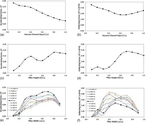
can be seen in Fig.3(a)that the accelerating factor gradually
decreases when the vacuum channel gapCincreases. Figure
3(b) shows that the deflecting factor drops with C for
C0.7kp, but it turns to increase whenC0.7kp. A channel gap ofC¼0.50kpis chosen as an acceptable parameter due
[image:3.607.79.269.56.264.2]to a trade-off between the accelerating gradient with a weak deflecting force and the available phase space in which high
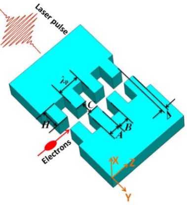
[image:3.607.313.555.57.238.2]FIG. 1. Schematic of a dual-grating structure.kp,A,B,C, H, andDrepresent grating period, dielectric pillar width, pillar trench, vacuum channel gap, pil-lar height, and longitudinal misalignment level, respectively.AþB¼kpis selected for all simulations.
FIG. 2. Longitudinal accelerating forceFzand a weak deflecting forceFyin a dual-grating structure illuminated by an input laser fieldE0 along the y-axis.
acceleration occurs. Figure 3(c) shows that the maximum
AF¼0.144 can be obtained at H¼0.80kpfor the structures
with a fixed C¼0.50kp, while the peak DF occurs at
H¼0.70kp as shown in Fig. 3(d). Fixing the grating,
C¼0.50kpandH¼0.80kp, we then set out to find the
opti-mal pillar width A and the longitudinal misalignment level D. The simulations sweep the pillar widthA from 0.10kpto
0.90kp combined with the variable misalignment D from
0.50kp to 0.50kp to obtain the optimum geometries. As
shown in Fig. 3(e), a global maximum accelerating factor
(AF¼0.170) can be easily found for a structure with
C¼0.50kp,A¼0.70kp,H¼0.80kp, andD¼0 nm. It is
inter-esting to note that the structures usually perform best when perfectly aligned (D¼0 nm), which can be seen in Figs.3(e)
and 3(f). This agrees well with the results from England
et al.30where they found that the weakest transverse deflect-ing force appeared for gratdeflect-ings with the perfect alignment. The damage threshold for quartz is about 1.5 J/cm2for laser pulses of 100 fs,31,32which is equivalent to an electric field ofEth¼9.0 GV/m, so the maximum achievable gradient for
a dual-grating structure is 0.1709.0¼1.53 GV/m.
III. BEAM QUALITY STUDY
A. Optimum structure geometry
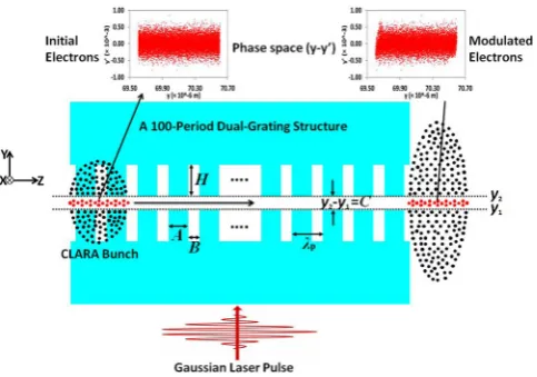
From optimizations in Section II, a dual-grating struc-ture withC¼0.50kp,H¼0.80kp, andA¼0.70kpwas found to be desirable as an optimum choice. Such optimized dual-grating structure with 100 periods as illustrated in Fig.5is chosen for the following beam quality studies, and the geom-etry parameters are summarized in TableI.
B. Laser parameters
In the simulation, a linearly polarized Gaussian laser
plane wave, as shown in Fig. 4, is launched to propagate
along the y-axis
Ez¼Epe
z wz
ð Þ2 2ln2 t
s
ð Þ2
cos 2ð pftÞ; (7)
where Ep,wz,s, and f represent the peak field, z-axis waist
[image:4.607.70.541.58.455.2]Em¼7.60 GV/m is still under the damage threshold, which
yields an unloaded gradientG¼1.29 GV/m according toG/
Em¼0.170 from the geometry optimization studies. In its
co-moving frame, the electrons experience a temporal electric
field Et¼Gpe
z wint
ð Þ2 with a characteristic interaction length
wint¼ w12 zþ
2ln2 bcs
ð Þ2 0:5
¼23lm. Integration of this field Et
with a peak accelerating gradient ofGp¼1.0 GV/m results in
a maximum energy gain ofDEm¼40 keV, which can be used
to calculate the accelerating gradient for subsequent
simulations.
C. Electron bunch parameters
CLARA will be a normal conducting linear electron accelerator capable of accelerating electrons to 250 MeV with a bunch charge of up to 250 pC. TableIIIshows the detailed
CLARA bunch parameters reproduced from Ref.22.
When CLARA works in an ultra-short pulse mode,22a
short electron bunch with a longitudinal RMS length of 9lm can be generated. When such a bunch is transmitted through the energy collimators, a bunch with a charge of 0.1 pC and an energy spread of 0.05% is expected. Then, it can be focused by a permanent quadrupole magnet to give a trans-verse RMS radius of 10lm, as presented in TableIIIbefore injecting into the optimum dual-grating structure. Here, the transverse size is much bigger than the vacuum channel gap
of 1lm, so only a small fraction of electrons traverse
through the vacuum channel of the structure. Those electrons travelling through the quartz substrate and grating pillars suf-fer significant energy loss due to collisional straggling33 in the dielectric material, so they are excluded in our following analysis. All of our simulations only focus on those electrons modulated by the laser field in the vacuum channel for analy-sis in terms of emittance and energy spread, which can be
seen in Fig.5. In addition, considering that electron energy of 50 MeV is highly relativistic, a space charge is not taken into account in our simulations.
D. The CLARA bunch travels through the optimum structure when laser is off
[image:5.607.49.294.70.165.2]In the first Particle-In-Cell (PIC) simulation, the CLARA electron bunch travels through the optimum struc-ture without interacting with the laser. The excited wakefield is reflected back by dielectric gratings and interacts with the bunch itself; this may result in energy loss or deflection of those electrons in the bunch tails in terms of its final emit-tance and energy spread. 500 000 macroparticles are used for our particle tracking simulations. It is found that about 4% of the 50 MeV bunch is transmitted through the vacuum
TABLE I. Geometry details of a 100-period dual-grating structure.
Geometry
Number of periods 100
Grating periodkp 2.0lm Vacuum channel gapC 1.0lm¼0.50kp Pillar heightH 1.6lm¼0.80kp Pillar widthA 1.4lm¼0.70kp Misalignment levelD 0.0 nm
[image:5.607.312.561.79.176.2]FIG. 4. The electric field envelope of the laser plane wave.
TABLE II. Parameters of the Gaussian laser plane wave used in the simulation.
Laser characteristics
Propagation direction þy
Wavelengthk 2lm
Peak laser fieldEp 5 GV/m
FWHM durations 100 fs
Waist radiuswz 50lm
[image:5.607.313.560.214.320.2]Frequencyf 150 THz
TABLE III. CLARA bunch parameters used in our simulation
Bunch parameters CLARA Simulation
Bunch energy (MeV) 50–250 50
Bunch charge (pC) 250 0.1
Bunch RMS length (lm) 9–300 9
Bunch RMS radius (lm) 10–100 10
Bunch density (m3) 1018–1022 4.41019
Normalized emittance (mmmrad) 1 0.2
Energy spread 0.01%–0.10% 0.05%
FIG. 5. Schematic of a CLARA electron bunch travelling through the opti-mum structure to interact with a Gaussian laser pulse, where the phase spaces for initial and modulated electrons are shown in subplots.
[image:5.607.316.558.557.726.2] [image:5.607.57.286.625.744.2]channel gap of 1.0lm. When the bunch travels out of the optimum structure, the charge is 3.9 fC, the transverse RMS normalized emittance is 5.5 nm, and the energy spread is 0.05% for those electrons between they1andy2planes (see
Fig.5). The final bunch energy spectrum as shown in Fig.6, which is calculated from the results of each individual parti-cle trace, indicates that the longitudinal wakefield has a weak force to the bunch itself after comparing with initial
spectrum. This could also be used to compare with that of the following laser-on case.
E. The CLARA bunch travels through the optimum structure when the laser is on
[image:6.607.68.541.56.611.2]In the second simulation scenario, the CLARA electron bunch is injected into the optimum structure to interact with
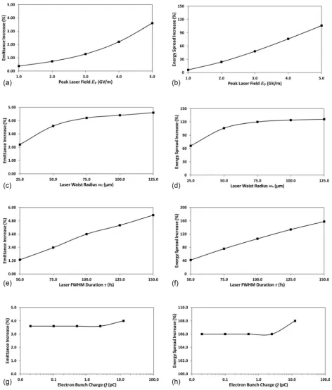
FIG. 6. Emittance ((a), (c), (e), and (g)) and energy spread ((b), (d), (f), and (h)) for modulated electrons as functions of a peak laser fieldEp(wz¼50lm,
the laser as summarized in Table II. From particle tracking simulations, it is found that the transverse RMS normalized emittance is 5.7 nm and the RMS energy spread is 0.103% for those modulated electrons when the bunch travels out of the structure (see Fig.5), corresponding to increases of 3.6% for emittance and 106% for energy spread compared to those of the laser-off case. With an RMS bunch length of 9lm, the electrons are able to sample all phases of the laser field in the channel gap, causing some electrons to gain energy from acceleration, while others are decelerated, which generates a big energy spread. The minor emittance difference may be explained by a weak deflecting force excited by the laser plane wave. However, it also indicates that the laser field inside the structure does not have an obvious effect on the final bunch transverse emittance at such short interaction length (wint ¼23lm).
Later, we study some factors influencing the final beam quality in terms of emittance and energy spread in detail. Figures6(a)and6(b)illustrate that the emittance and energy spread rise with a larger peak laser field, which induces a stronger accelerating and deflecting field for electrons to experience. For a peak laser field of 1 GV/m, small increases of 0.4% for emittance and 6% for energy spread are expected, but at the cost of a reduced accelerating gradient. With a bigger laser waist radius and FWHM duration, the emittance and energy spread increase as shown in Figs. 6(c)–6(f). This is expected since the interaction lengthwintis
related to laser waist radius and FWHM duration. Figures
6(g) and 6(h) show that the emittance and energy spread
remain constant when the bunch charge Q is between
0.02 pC and 2.5 pC, and increase when Q>2.5 pC, which corresponds to a bunch density of 1.11021/m3. This means that a bunch density higher than 1.11021/m3can excite a stronger longitudinal and transverse wakefield, which results in larger emittance and energy spread. Based on these analy-ses, a high peak laser field with long waist radius and FWHM duration is preferred to achieve a considerable energy gain in a long-range acceleration; however, the resulting emittance increase could be an issue. A low bunch density of<1.11021/m3is desired to load into such a dual-grating structure to interact with laser pulses, in which a small emittance increase of3.6% can be achieved. In addi-tion, the deflecting force can be compensated for by symmet-ric illumination using two laser beams from opposite sides.
The CLARA electron bunch can be partitioned into a series of short slices of length Dt k0/c. After interacting
with the sinusoidal electric field in the channel gap of the structure, each slice of the electron bunch experiences a net energy shift described by
gðDt;DEÞ ¼DEcos 2pc
k0
Dt
; (8)
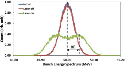
whereDEis the maximum energy gain for the electrons. For a bunch with a Gaussian distributed energy spectrum, when all contributions from each slice are superimposed, it is eas-ily predicted that the energy spectrum will be changed to a double-peaked profile,26as shown in Fig.7. It demonstrates
that the maximum energy gain is DE¼4566 keV,
corre-sponding to a maximum accelerating gradient of G¼1.13
60.15 GV/m. Given that the maximum electric field Em
¼7.60 GV/m in the structure observed from VSim, the accel-erating factor AF¼G/Em¼0.14960.020 can be compared
with the unloadedAF¼0.170 from the finite-difference time-domain simulation for dual-grating structures.
IV. CONCLUSION
This paper presents detailed beam quality studies for an optimized 100-period dual-grating structure in terms of the emittance, energy spread, and loaded accelerating gra-dient. In order to get the optimum geometry, we have car-ried out studies to maximize the accelerating factor for quartz dual-grating structures. For dual-grating structures with a vacuum channel gap of half laser wavelength illumi-nated by a single laser beam, a maximum accelerating
fac-tor AF¼0.170 can be obtained, corresponding to a
maximum unloaded gradient of G¼1.53 GV/m. Using
VSim, a realistic CLARA electron bunch with a
longitudi-nal bunch length of 9lm and a transverse RMS size of
10lm is loaded into the optimum dual-grating structure to interact with a realistic laser pulse. Our numerical simula-tions only focus on electrons travelling through the vac-uum channel to interact with laser field. In this case, when the modulated electrons travel out of the structure, the transverse normalized emittance increases by 3.60% com-pared to that of laser-off case, the energy spread changes from 0.05% to 0.103%, and an accelerating gradient up to
1.1360.15 GV/m could be expected from the particle
tracking simulations. In addition, we also analyze the effect of laser parameters and electron density on the beam quality in detail. When electrons interact with a higher peak laser field with longer waist radius and FWHM dura-tion, it can lead to the increase of emittance and energy
spread. However, a low electron bunch density of <1.1
1021/m3is desired to generate a small emittance increase
of3.6%.
These simulation results not only theoretically demon-strate the capabilities of a dual-grating DLA with good beam quality but also numerically predict the realistic DLA experi-ment results in terms of emittance, energy spread, and loaded gradient. However, the energy gain in our simulations is lim-ited by the laser-electron interaction length. A
pulse-front-FIG. 7. Bunch energy spectrum for initial electrons and modulated electrons with the laser off and on. Electrons travelling through the quartz substrate and grating pillars are not shown in this figure.
[image:7.607.64.284.611.726.2]tilt operation for a laser beam will be considered as part of future studies to extend the interaction length, thereby result-ing in a greater energy gain for a DLA.
Dual-grating structures have been fabricated at the Laboratory for Micro and Nanotechnology, PSI (Paul Scherrer Institute). They will be tested with beam in 2017 and benchmarked against results from simulations to further optimize both the structure and the acceleration process overall.
ACKNOWLEDGMENTS
We would like to thank Dr. Lee Devlin for carefully proof reading the original manuscript and Dr. Rasmus Ischebeck, Dr. Micha Dehler, Dr. Eugenio Ferrari, and Dr. Nicole Hiller for many useful discussions. This work was supported by the EU under Grant Agreement No. 289191, the STFC Cockcroft Institute core Grant No. ST/G008248/1.
1J. Norem, V. Wu, A. Moretti, M. Popovic, Z. Qian, L. Ducas, Y. Torun, and N. Solomey,Phys. Rev. Spec. Top. Accel. Beams6, 072001 (2003). 2
A. Moretti, Z. Qian, J. Norem, Y. Torun, D. Li, and M. Zisman,Phys.
Rev. Spec. Top. Accel. Beams8, 072001 (2005).
3M. R. Jana, M. Chung, M. Leonova, A. Moretti, A. Tollestrup, and K. Yonehara, in Proceedings of PAC2013, Pasadena, CA, USA, p. WEPMA12. 4
T. Plettner, P. P. Lu, and R. L. Byer,Phys. Rev. Spec. Top. Accel. Beams
9, 111301 (2006).
5A. Aimidula, M. A. Bake, F. Wan, B. S. Xie, C. P. Welsch, G. Xia, O. Mete, M. Uesaka, Y. Matsumura, M. Yoshida, and K. Koyama, Phys.
Plasmas21, 023110 (2014).
6
A. Aimidula, C. P. Welsch, G. Xia, K. Koyama, M. Uesaka, M. Yoshida, O. Mete, and Y. Matsumura,Nucl. Instrum. Methods Phys. Res., Sect. A
740, 108 (2014). 7
C. M. Chang and O. Solgaard,Appl. Phys. Lett.104, 184102 (2014). 8
X. E. Lin,Phys. Rev. Spec. Top. Accel. Beams4, 051301 (2001). 9V. Reboud, J. Romero-Vivas, P. Lovera, N. Kehagias, T. Kehoe, G.
Redmond, and C. M. S. Torres, “Lasing in nanoimprinted two-dimensional photonic crystal band-edge lasers,” Appl. Phys. Lett.102, 073101 (2013).
10B. M. Cowan,Phys. Rev. Spec. Top. Accel. Beams6, 101301 (2003). 11Z. Wu, R. J. England, C. K. Ng, B. Cowan, C. McGuinness, C. Lee, M. Qi,
and S. Tantawi,Phys. Rev. Spec. Top. Accel. Beams17, 081301 (2014). 12
T. Plettner and R. L. Byer, Phys. Rev. Spec. Top. Accel. Beams11, 030704 (2008).
13K. Soong and R. L. Byer,Opt. Lett.
37, 975–977 (2012). 14
T. Plettner, R. L. Byer, C. McGuinness, and P. Hommelhoff,Phys. Rev.
Spec. Top. Accel. Beams12, 101302 (2009).
15
E. A. Peralta, K. Soong, R. J. England, E. R. Colby, Z. Wu, B. Montazeri, C. McGuinness, J. McNeur, K. J. Leedle, D. Walz, E. B. Sozer, B. Cowan, B. Schwartz, G. Travish, and R. L. Byer,Nature503, 91 (2013).
16K. P. Wootton, Z. Wu, B. M. Cowan, A. Hanuka, I. V. Makasyuk, E. A. Peralta, K. Soong, R. L. Byer, and R. J. England,Opt. Lett.41, 2696–2699 (2016).
17J. Breuer and P. Hommelhoff,Phys. Rev. Lett.111, 134803 (2013). 18
K. J. Leedle, R. F. Pease, R. L. Byer, and J. S. Harris,Optica 2, 158 (2015).
19K. J. Leedle, A. Ceballos, H. Deng, O. Solgaard, R. F. Pease, R. L. Byer, and J. S. Harris,Opt. Lett.40, 4344–4347 (2015).
20
Y. Wei, C. P. Welsch, G. Xia, O. Mete, K. Hanahoe, and J. D. A. Smith, in Proceedings of the IPAC2015, Richmond, VA, USA, p. WEPWA051. 21B. Montazeri Najafabadi, R. L. Byer, C. K. Ng, R. J. England, E. A.
Peralta, K. Soong, R. Noble, and Z. Wu, AIP Conf. Proc. 1507, 476 (2012).
22J. A. Clarke, D. Angal-Kalinin, N. Bliss, R. Buckley, S. Buckley, R. Cash, P. Corlett, L. Cowie, G. Cox, G. P. Diakun, D. J. Dunning, B. D. Fell, A. Gallagher, P. Goudket, A. R. Goulden, D. M. P. Holland, S. P. Jamison, J. K. Jones, A. S. Kalinin, W. Liggins, L. Ma, K. B. Marinov, B. Martlew, P. A. McIntosh, J. W. McKenzie, K. J. Middleman, B. L. Militsyn, A. J. Moss, B. D. Muratori, M. D. Roper, R. Santer, Y. Saveliev, E. Snedden, R. J. Smith, S. L. Smith, M. Surman, T. Thakker, N. R. Thompson, R. Valizadeh, A. E. Wheelhouse, P. H. Williams, R. Bartolini, I. Martin, R. Barlow, A. Kolano, G. Burt, S. Chattopadhyay, D. Newton, A. Wolski, R. B. Appleby, H. L. Owen, M. Serluca, G. Xia, S. Boogert, A. Lyapin, L. Campbell, B. W. J. McNeil, and V. V. Paramonov,J. Instrum.9, T05001 (2014).
23R. B. Palmer, Part. Accel.
11, 81–90 (1980); available athttp://cds.cern.ch/ record/1107986/files/p81.pdf.
24
D. M. Pai and K. A. Awada,Opt. Soc. Am. A8, 755–762 (1991). 25J. Breuer, J. McNeur, and P. Hommelhoff,J. Phys. B: At. Mol. Opt. Phys.
47, 234004 (2014). 26
E. A. Peralta, “Accelerator on a chip: Design, fabrication, and demonstra-tion of grating-based dielectric microstructures for laser-driven accelera-tion of electrons,” Ph.D. thesis (Stanford University, 2015).
27
Seehttps://www.txcorp.com/vsimfor VSim.
28
T. Plettner, R. L. Byer, and B. Montazeri,J. Mod. Opt.58, 1518 (2011). 29R. Kitamura, L. Pilon, and M. Jonasz,Appl. Opt.46, 8118 (2007). 30R. J. England, R. J. Noble, K. Bane, D. H. Dowell, C.-K. Ng, J. E.
Spencer, S. Tantawi, Z. Wu, R. L. Byer, E. Peralta, K. Soong, C. Chang, B. Montazeri, S. J. Wolf, B. Cowan, J. Dawson, W. Gai, P. Hommelhoff, Y. Huang, C. Jing, C. McGuinness, R. B. Palmer, B. Naranjo, J. Rosenzweig, G. Travish, A. Mizrahi, L. Schachter, C. Sears, G. R. Werner, and R. B. Yoder,Rev. Mod. Phys.86, 1337 (2014).
31M. Lenzner, J. Kr€uger, S. Sartania, Z. Cheng, Ch. Spielmann, G. Mourou, W. Kautek, and F. Krausz,Phys. Rev. Lett.80, 4076 (1998).
32
K. Soong, R. L. Byer, C. McGuinness, E. Peralta, and E. Colby, in
Proceedings of 2011 Particle Accelerator Conference (PAC2011)(IEEE, New York, USA, 2011), p. MOP095.
33