Precise Modication of 2D Materials by
Gas Ion Beams
A thesis submitted in fullment of the requirements for the degree of
Doctor of Philosophy in the
School of Physics
Trinity College Dublin
September 2017
Author
Supervisor
Declaration
I declare that this thesis has not been submitted as an exercise for a degree at this or any other university and it is entirely my own work.
I agree to deposit this thesis in the university's open access institutional repository or allow the library to do so on my behalf, subject to Irish copyright legislation and Trinity College Library conditions of use and acknowledgement.
Elements of this work that have been carried out jointly with others or by collabo-rators have been duly acknowledged.
I have read and I understand the plagiarism provisions in the General Regulations of the University Calendar for the current year, found at: http://www.tcd.ie/calendar.
I have also completed the online tutorial on avoiding plagiarism Ready, Steady, Write, located at http://tcd-ie.libguides.com/plagiarism/ready-steady-write.
Abstract
Precise Modication of 2D Materials by Gas Ion Beams
Pierce Maguire
Precise modication of the geometry, stoichiometry and crystal structure of two dimensional (2D) materials will be instrumental in future nanodevice fabrication. Here, ion beams focused to a sub-nanometre scale have been demonstrated to mod-ify the electrical and optical properties of graphene and molybdenum disulphide (MoS2). Nanopores with sub-5 nm diameters were fabricated in graphene using a ni-trogen gas-etching process moderated by an electron beam. A diusion-based model was developed to quantify and illuminate the process. Defect-engineering was per-formed in graphene with a high level of precision by irradiation with He+ and Ne+.
Separately the defect-engineering process was expanded for monolayer MoS2. Irra-diation was also used to fabricate nanostructures with nanometre scale widths, to tune stoichiometry and to alter resistivity. Imaging using high resolution transmis-sion electron microscopy demonstrated high quality He+ ion fabricated nanoribbons
Research Output
Publications
The following is a list of the author's scientic output at time of publication. Numbers 3, 10 and 15 and the papers in preparation (17 and 18) are highlighted as contributing a great deal to this thesis.
1. R. O'Connell, Yanhui Chen, Hongzhou Zhang, Yangbo Zhou, Daniel S. Fox, Pierce Maguire, Jing Jing Wang, Cornelia Rodenburg.
Comparative study of image contrast in scanning electron microscope and helium ion microscope, Journal of Microscopy, 268 (3), December 2017
2. Yanhui Chen, Fei Xue, Shengcheng Mao, Haibo Long, Bin Zhang, Qingsong Deng, Bin Chen, Yinong Liu, Pierce Maguire, Hongzhou Zhang, Xiaodong Han, and Qiang Feng.
Elemental preference and atomic scale site recognition in a Co-Al-W-base su-peralloy, Scientic Reports, 7 (1), December 2017
3. Pierce Maguire, Daniel S. Fox, Yangbo Zhou, Qianjin Wang, Maria O'Brien, Jakub Jadwiszczak, John McManus, Niall McEvoy, Georg S. Duesberg, Hongzhou Zhang.
Defect sizing, distance and substrate eects in ion-irradiated monolayer 2D materials, arXiv.org, 1707.08893, July 2017
Ferreira, A. Louise Bradley, John J. Boland, Georg S. Duesberg, Valeria Ni-colosi, Hongzhou Zhang.
Oxide-mediated recovery of eld eect mobility in plasma-treated MoS2, Sci-ence Advances, Accepted for publication, January 2018.
arXiv.org, 1706.08573, June 2017
5. Yanhui Chen, Junfeng Zhou, Felim Vajda, Pierce Maguire, Robert O'Connell, Wolfgang Schmitt, Yonghe Li, Zheng-Guang Yan, Yue-Fei Zhang, Hongzhou Zhang.
Multi-metallic hydrate hollow structures in cobalt hydrate based systems, Crystal Growth & Design, 17 (4), March 2017
6. Wei Lu, Alan Kelly, Pierce Maguire, Hongzhou Zhang, Catherine Stanton, Song Miao.
Correlation of emulsion structure with cellular uptake behaviour of encapsu-lated bioactive nutrients: inuence of droplet size and interfacial structure, Journal of Agricultural and Food Chemistry, 64 (45), October 2016
7. Junfeng (Jim) Zhang, Ki-Bum Lee. Linchen He, Joanna Seiert, Prasad Sub-ramaniam, Letao Yang, Shu Chen, Pierce Maguire, Gediminas Mainelis, Stephan Schwander, Teresa Tetley, Alexandra Porter, Mary Ryan, Milo Shaf-fer, Sheng Hu, Jicheng Gong, Kian Fan Chung.
Eects of a nanoceria fuel additive on the physicochemical properties of diesel exhaust particles, Environmental Science Processes & Impacts, 18 (10), September 2016
8. Yangbo Zhou, Pierce Maguire, Jakub Jadwiszczak, Manoharan Muru-ganathan, Hiroshi Mizuta, Hongzhou Zhang,
Precise milling of nano-gap chains in graphene with a focused helium ion beam, Nanotechnology, 27 (32), June 2016
9. Junfu Ji, Kevin Cronin, John Fitzpatrick, Pierce Maguire, Hongzhou Zhang, Song Miao,
powders: The eect of granule growth in the high shear granulation process Journal of Food Engineering, 189, May 2016
10. Daniel S. Fox, Pierce Maguire, Yangbo Zhou, Cornelia Rodenburg, Arlene O' Neill, Jonathan N. Coleman, Hongzhou Zhang,
Sub-5 nm graphene nanopore fabrication by nitrogen ion etching induced by a low-energy electron beam Nanotechnology, 27 (19), May 2016
11. Junfu Ji, John Fitzpatrick, Kevin Cronin, Pierce Maguire, Hongzhou Zhang, Song Miao,
Rehydration behaviours of high protein dairy powders: The inuence of ag-glomeration on wettability, dispersibility and solubility Food Hydrocolloids, 58, March 2016
12. Yangbo Zhou, Daniel S. Fox, Pierce Maguire, Robert O'Connell, Robert Masters, Cornelia Rodenburg, Hanchun Wu, Maurizio Dapor, Ying Chen, Hongzhou Zhang,
Quantitative secondary electron imaging for work function extraction at atomic level and layer identication of graphene, Scientic Reports, 6, Febru-ary 2016
13. Yanhui Chen, Junfeng Zhou, Pierce Maguire, Robert O'Connell, Wolfgang Schmitt, Yonghe Li, Zhengguang Yan, Yuefei Zhang, Hongzhou Zhang, Enhancing capacitance behaviour of CoOOH nanostructures using transition metal dopants by ambient oxidation, Scientic Reports, 7, February 2016
14. Askar Syrlybekov, Han-Chun Wu, Ozhet Mauit, Ye-Cun Wu, Pierce Maguire, Abbas Khalid, CormacO´ Coile´ain, Leo Farrel, Chenglin Heng, Mohamed Abid, Huajun Liu, Li Yang, Hongzhou Zhang, Igor V. Shvets,
Electrical-eld-driven metal-insulator transition tuned with self-aligned atomic defects, Nanoscale, 7 (33), July 2015
Jonathan N. Coleman, John F. Donegan, Hongzhou Zhang, Nanopatterning and electrical tuning of MoS2 layers with a sub-nanometre helium ion beam," Nano Letters, 15 (8), July 2015
16. Yangbo Zhou, Robbie O'Connell, Pierce Maguire, Hongzhou Zhang, High throughput secondary electron imaging of organic residues on a graphene surface," Scientic Reports, 7032 (4), November 2014
In Preparation
17. Pierce Maguire, Maria O'Brien, Niall McEvoy, Georg S. Duesberg, Hongzhou Zhang, Defect density dependence of low frequency Raman spectroscopy modes in ion irradiated bilayer MoS2," In Preparation, 2017
18. Pierce Maguire, Maria O'Brien, Jakub Jadwiszczak, Darragh Keane, Daniel S. Fox, Niall McEvoy, John Boland, Georg S. Duesberg, Hongzhou Zhang, Ion moderated oxidative etching of MoS2," In Preparation, 2017
Presentations
• Ne+, He+ andGa+ Irradiation for Nanometre Tuning of 2D Materials,
Pre-sented at MMC 2015, Manchester, UK and MSI 2015, University of Limerick.
• Evolution of the Raman spectra of graphene and MoS2with scanningHe+ and
Ne+ irradiation. Presented at MSI Comerford Memorial poster session, 2017,
Acknowledgements
First and foremost, my sincere thanks to past and present members of the Photonics and Nanofabrication Group for their training, expertise and very signicant contri-bution to my training and research. I am grateful to my mentor Dr. Daniel S. Fox for his assistance and guidance. Special thanks are also due to Prof. Yangbo Zhou, Prof. Yanhui Chen, Abbas Khalid, Dr. Robert O'Connell, Junfeng Zhou, Darragh Keane, Fei Gao, Jakub Jadwiszczak, Gen Li and other students who joined us briey. Above all, sincere thanks to my supervisor, Prof. Hongzhou Zhang for his patience and support.
I wish to thank the sta and students of the School of Physics, particularly Dr. Niamh McGoldrick, Prof. Cormac McGuinness and the Photonics Group. Many of the sta of CRANN/AMBER have provided essential assistance, especially at the Advanced Microscopy Laboratory: Dermot Daly; Clive Downing; Dr. Alan Bell; Cathal McAuley; Keith Boland; Dr. Allen Bellew, Dr. Eoin McCarthy and Dr. Clodagh Dooley. Several collaborators deserve special mention for their enormous help and support including members of the ASIN group in the School of Chemistry including Dr. Maria O'Brien and Dr. Niall McEvoy, and Qianjin Wang at the Collaborative Innovation Center of Advanced Microstructures at Nanjing University. Of my friends, colleagues and extended family I thank Mary Matthews and members of Prof. Nicolosi's group with particular mentions to Dr. Anuj Pokle, Megan Canavan and Dr. Edmund Long.
Contents
Declaration iii
Abstract v
Research Output vii
Acknowledgements xi
Contents xii
List of Figures xvii
List of Tables xxi
Glossary xxiii
1 Introduction 1
1.1 Outline of the Thesis . . . 4
2 Materials 7
2.1 Graphene . . . 7 2.2 Molybdenum Disulphide . . . 15
3 Modication Methodology 23
3.4 Simulating Ion Interactions . . . 28
3.5 Dose and Substrate Eects . . . 29
3.6 Displacement Threshold in MoS2 . . . 31
3.7 Ion Beams and 2D Materials . . . 32
3.8 Electron Beams and Defects . . . 33
3.9 Oxidation of FLM-MoS2 in the Literature . . . 33
4 Analysis Methodology 43 4.1 Raman Spectroscopy . . . 43
4.2 Low Frequency Raman Spectroscopy of MoS2 . . . 48
4.3 Photoluminescence Spectroscopy . . . 49
4.4 Microscopy and Resolution . . . 50
4.5 Scanning Electron Microscope . . . 50
4.6 Transmission and Scanning Transmission Electron Microscopy . . . . 53
4.7 Energy Dispersive X-ray Spectroscopy . . . 55
5 Modifying Graphene by Charged Particle Beams 57 5.1 Electron Beam-Induced Nitrogen Etching . . . 58
5.1.1 Summary . . . 67
5.2 Defect-Engineering byHe+ and Ne+ Irradiation . . . 68
5.2.1 Summary . . . 80
6 Irradiation and Patterning of MoS2 81 6.1 Structural Modication and Defect-Engineering . . . 82
6.2 Stoichiometry Tuning . . . 90
6.3 Nanostructure Fabrication . . . 92
6.4 Electrical Characterisation . . . 95
6.5 Summary . . . 100
7 Ion Moderated Oxidation of MoS2 101 7.1 Ion Dose Dependency . . . 101
7.2 Expanding the Oxidation Model . . . 104
CONTENTS
7.4 Etching Range and Edge Denition . . . 115 7.5 Summary . . . 116
8 Conclusion 119
8.1 Future Work . . . 120
Appendices 121
A Identifying Suitable Samples in TMSEM 123
B Supplementary Information for Etching of Graphene by Nitrogen 125
C Ion Beam Stability and Dose Uncertainty 131
D Fitting the LA(M) Mode in Raman 133
E Probe Size Measurement in the GIM 135
F Oxidative Etching Attempts with Mechanically Exfoliated MoS2 137
G Producing Meshes with Oxidation 139
List of Figures
2.1 Graphene lattice and 2D band generation from transition sliding. . . 8
2.2 The calculated phonon dispersion relation of graphene . . . 10
2.3 Double and triple resonance in Raman spectra of graphene . . . 11
2.4 D band generation from regions adjacent to defect sites . . . 14
2.5 Evolution of the 2D peak as a function of number of layers . . . 16
2.6 The Brillouin zone and band structure of MoS2 . . . 18
2.7 The crystal structure of monolayer MoS2 . . . 18
2.8 Vibrational modes and Raman spectroscopy for the dierentiation of the number of MoS2 layers . . . 20
3.1 The gas eld ion source in the gas ion microscope . . . 26
3.2 A Stopping and Range of Ions in Matter software simulation of ion trajectories. . . 29
3.3 Displacement cross sections of atoms in MoS2 with 30 keV He+ . . . . 31
3.4 Thermal thinning and etching of 2L MoS2 nanosheets . . . 37
3.5 Modelling the etching of triangular pits in MoS2 . . . 39
4.1 Jablonski diagram illustrating Stokes and anti-Stokes shifts . . . 44
4.2 Data treatment in Raman spectroscopy . . . 47
4.3 Low frequency Raman spectrum and peak intensity map of the layer breathing mode of 2L MoS2 . . . 49
4.4 Outline of a scanning electron microscope . . . 51
5.1 SEM images of electron-irradiated graphene with and without nitrogen gas . . . 59 5.2 TEM images of electron beam-assisted nitrogen etched graphene . . . 61 5.3 Etching and deposition rates as a function of beam current. . . 62 5.4 The area of graphene etched as a function of electron beam dwell time. 65 5.5 Nitrogen etching rate as a function of beam current . . . 66 5.6 MoS2 ake after an etching attempt with nitrogen gas. . . 67 5.7 Representative selection of irradiated CVD graphene Raman spectra . 69 5.8 Evolution of the full width at half maximum of theG peak and
inten-sity ratio in graphene . . . 70 5.9 The2D peak in graphene Raman spectra . . . 71 5.10 The evolution of the ID/IG ratio of freestanding and supported
graphene with LD . . . 72 5.11 Graph of defect size against the maximum of theID/IG peak . . . 75
6.1 Modication of few layer mechanically exfoliated MoS2 crystal struc-ture with He+ imaged in TEM . . . 82
6.2 Low frequency Raman modes in bilayer MoS2 . . . 84 6.3 Ion dose dependent photoluminescence spectroscopy of bilayer MoS2 . 87 6.4 Representative selection of Raman spectra of irradiated monolayer MoS2 88 6.5 Evolution of the FWHM and peak position withLD(Miд) for monolayer
MoS2 . . . 88 6.6 Evolution of the Ratios of the intensity of the LA(M) peak to the
intensity of the E0 and A0
1 modes for both He+ and Ne+ irradiated monolayer MoS2. . . 89 6.7 Stoichiometry alteration of a few layer MoS2 ake by He+ irradiation. 91 6.8 HRTEM images of the edges of three regions in the same freestanding
MoS2 ake milled with three dierent probe sizes. . . 92 6.9 Graph of simulated ion distribution at nanostructure edges with ratio
of FFTs . . . 94 6.10 TEM images ofHe+ fabricated few layer freestanding nanoribbons in
6.11 Simulation of the distribution of ion dose produced by a Gaussian array. 96
6.12 Electrical characterization of He+ modied devices. . . 97
6.13 Electrical characterization of He+ manufactured 20 nm nanoribbon. . 99
7.1 Outline of a typical oxidative etching experiment . . . 102
7.2 Ion dose dependency of oxidative etching in bilayer MoS2 . . . 104
7.3 Scanning electron microscopy analysis of etching bilayer MoS2 in a cumulative heating experiment. . . 105
7.4 Searching for MoOx in heated CVD MoS2 using Raman spectroscopy 107 7.5 Expanding the etching model for monolayer CVD MoS2 with Raman spectroscopy. . . 109
7.6 Heat maps of SEM brightness and A0 1 peak position and width for bilayer MoS2. . . 112
7.7 Edge roughness and etching range . . . 114
A.1 Identifying suitable MoS2 akes for experiments in TMSEM. . . 124
B.1 Mono and ten layer graphene etch . . . 126
B.2 Optical image of single and ten layer MoS2 on a 300 nm SiO2 layer on Si. . . 126
B.3 Temperature eect of e-beam etching. . . 128
B.4 Measuring nanopore sizes from TEM images with Imagej . . . 129
D.1 Raman spectra with tting of the LA(M)mode . . . 134
E.1 Measuring probe size from a GIM image . . . 136
F.1 Attempted etching of mechanically exfoliated MoS2 . . . 138
List of Tables
3.1 Key gures from the literature concerning the oxidation of MoS2 . . . 40
5.1 Sputtering yields and defect per incident ion values of carbon atoms in graphene . . . 73 5.2 Initial tting parameters for use with the modied version of the model
developed by Lucchese et al. . . 74 5.3 Key gures calculated from tting the model developed by Lucchese
et al. . . 74 5.4 Comparison of three ion species at 30 keV. . . 78
Glossary
A number of abbreviations, important terms and chemical formulae are listed. Please note that for the purposes of the glossary, the words microscope and microscopy can be considered interchangeable and dependent on context.
2D two dimensional ii, 14, 6, 14, 2022, 28, 40, 47, 49, 50, 53, 76, 77, 97, 113115 AC armchair-terminated edge 36
AFM atomic force microscopy 33, 34, 54, 78
Amorphous Carbon carbon without crystal structure 43
BID beam-induced deposition 43 BIV best imaging voltage 24 BSE backscattered electrons 48, 49 CLS cathodoluminescence spectroscopy 48, 52
CVD chemical vapour deposition 8, 16, 22, 64, 69, 79, 82, 97, 98, 100, 110, 129 Defect-Engineering controlled alter-ation of the defect density or type of de-fects in a material ii, 25, 14, 22, 25, 30, 32, 77, 97, 114, 115
DFT density functional theory 2, 17, 18,
22, 27, 33, 34, 36
Displacement Threshold minimum ki-netic energy that an atom in a solid needs to be permanently displaced from its lat-tice site 29
Double-Resonance a fourth-order per-turbative Raman model used in carbon materials 10, 11
EBL electron beam lithography 92 EDX energy dispersive x-ray spec-troscopy 4, 40, 48, 52, 79, 86, 94
EELS electron energy loss spectroscopy 52
EFTEM energy-ltered transmission electron microscopy 122
ET Everhart-Thornley 49, 50 FeSi2 iron disilicide 94
FET eld eect transistor 32
FIB focused ion beam 3, 23, 25, 121 FLG few layer graphene 56, 58
FLM few layer or monolayer 32, 33, 112 Fullerene hollow molecules of carbon 42 FWHM full width at half maximum 43, 66, 67, 89
GFIS gas eld ion source 3, 24, 25 GIM gas ion microscope 24, 25, 4749, 51, 97, 100, 114, 117
Graphene 2D honeycomb lattice of sp2 carbon atoms ii, 2, 4, 6, 8, 9, 1114, 16, 18, 23, 29, 30, 32, 40, 42, 43, 53, 54, 56, 58, 62, 64, 67, 69, 71, 73, 74, 76, 77 HAADF high angle annular dark eld 6, 51, 86
HOPG highly oriented pyrolitic graphite 8
ImageJ image processing program with many available plugins 56, 127
Inter-defect distance average distance between defects 4, 13, 54, 7678, 85 IR infrared 18
ITO indium tin oxide 8
KHD Kramers-Heisenberg-Dirac 11 LBM layer breathing mode 42, 45, 79, 81 LMIS liquid metal ion source 23
Matlab a programming language and computing environment developed by Mathworks 73, 131
MFM magnetic force microscopy 33, 34 MgO magnesium oxide 26
Molecular Dynamics computer
simu-lation method for atom/ion interactions 21, 27
MoO2 molybdenum dioxide 102104 MoO3 molybdenum trioxide 3234, 38, 79, 102104, 109, 111
MoOx molybdenum oxide 38, 39, 97 MoS2molybdenum disulphide ii, xii, xiii, 16, 14, 16, 18, 19, 2123, 26, 2836, 38 40, 42, 43, 45, 47, 5254, 62, 63, 7779, 81, 82, 8486, 88, 89, 91, 92, 94100, 102 115, 119, 129, 131
MoSe2 molybdenum diselenide 45 MoTe2 molybdenum telluride 94
Nanoribbon strips of material of thick-ness <100 nm 23, 27, 77, 95
NMP N-methyl-pyrrolidone 54 O2 molecular oxygen 32, 34
OM optical microscopy 34, 47, 48, 79, 97, 99, 129
PL photoluminescence spectroscopy 16, 34, 40, 47, 81
RPM rotations per minute 54
RT room temperature 99, 104, 106, 107, 109
SCCM standard cubic centimetres per minute (unit of ow rate) 79
SE secondary electron 4850 SE1 type 1 4850
SE2 type 2 49 SE3 type 3 49
Glossary
107111, 113, 117, 119, 121, 122, 131 SES secondary electron spectroscopy 48 SFIM scanning eld ion microscopy 24 SiO2 silicon dioxide 34, 54, 91, 119, 129 SM shear mode 42, 45, 79, 81
SO2 sulphur dioxide 32
SRIM Stopping and Range of Ions in Matter software 21, 2628, 69, 71, 73 STEM scanning transmission electron microscope 6, 50, 51, 79, 86, 117
TEM transmission electron microscope ii, 3, 4, 23, 40, 50, 51, 54, 5658, 78, 79, 88, 89, 117, 121, 122, 127
TMD transition metal dichalcogenide 1, 14, 18, 32, 45, 115
TMSEM transmission mode scanning electron microscopy 50, 56, 86, 117 TR triple resonance 10
TTL through the lens 4850, 100 WS2 tungsten disulphide 30, 47 WSe2 tungsten diselenide 45 XeF2 xenon diuouride 62
XPS X-ray photoelectron spectroscopy 34
ZZ zig-zag terminated edge 36
ZZ-Mo Mo terminated zig-zag edge 36, 38
Chapter 1
Introduction
T
wo dimensional materials were brought to global attention by Geim and Novoselov in 2004, who would later share the 2010 Nobel Prize in Physics for their work on graphene [1]. The structure of graphene was rst discussed by Wal-lace as early as 1947 and its name was coined by Boehm et al. in 1994 [24]. Geim and Novoselov succeeded in isolating, visualising and characterising this material of single atom thickness from graphite.The extraordinary properties of graphene are now well-documented and are in large part responsible for stimulating the discovery of a wide variety of 2D materials and related research methodologies under investigation today [5, 6]. The extraordi-nary properties and tunability of 2D materials have been repeatedly demonstrated, heralding a new era of materials science [1, 6]. The physical properties of 2D ma-terials are highly distinguished with respect to their bulk counterparts due to the evolution of their band structure with layer number [59]. MoS2 for instance, is a quintessential transition metal dichalcogenide (TMD) which has an indirect band gap in the multi-layer system and a direct band gap in the monolayer. This allows a vast enhancement in radiative recombination, essential for the use of a material in optoelectonic devices such as thin lm photodetectors [1012]. Proposed applica-tions of 2D materials are in elds as diverse as photonics, electronics and composites [13, 14].
Moore's law will shortly require the downsizing of transistors in computational de-vices to a scale of single digit nanometres. Bulk silicon, the incumbent material in this eld for many decades, is expected to be unable to reach the smallest possible size range and still maintain performance due to severe short channel eects [15]. If Moore's law is to continue, it appears at this juncture that enabling technolo-gies may have to incorporate the extraordinary family of 2D materials. However, given their diminutive scale a host of novel fabrication methodologies must be em-ployed for these materials to become functional devices. Fabrication technologies must produce future-devices while also achieving acceptable throughput and cost-eectiveness. Nanometre-scale tuning of behaviour must also be accompanied by minimal structural damage. Other challenges regarding the material properties in-clude opening and controlling band gaps (for example in zero band gap graphene) and controlling doping states (for example achieving p-type doping of MoS2) while maintaining high mobility [6, 16].
materials [2629].
The demands of modern semiconductor technology are such that precise nanoscale control of 2D material properties is much sought after. However, scalable nanofabri-cation methods to produce such structures remain elusive. To date, many chemical and physical methods have been used to produce MoS2nanostructures with a desired geometry. These approaches have produced nanoribbons that were either polycrys-talline or too wide (>10 nm) [30, 31]. Direct fabrication of MoS2 nanoribbons down to 0.44 nm has been reported in a transmission electron microscope (TEM) [32] al-though the composition and phase of these structures is the subject of continued discussion [33]. This is also an impractical fabrication approach due to its require-ment of a freestanding sample, its low rate of milling, lack of scalability, and its expense. A Ga+ focused ion beam (FIB) can sputter surface atoms and introduce
nanoscale modication eectively with its∼5 nm probe [34]. However, a non-metallic ion species and a sub-nanometre probe size are required for the high resolution ma-chining of semiconducting devices.
Recently, ion microscopes using a gas eld ion source (GFIS) have made these goals eminently achievable due to their sub-nanometre resolution and relatively high throughput [3540]. Given the superlative connement of 2D materials in their out-of-plane direction, it is possible to restrict the ion-induced interaction in this direction to their exceptionally small thickness. Ion irradiation can be used to perform a wide range of alterations beyond introducing defects and sputtering. He+ irradiation of
graphene encapsulated in hexagonal boron nitride has been used to introduce n-type doping [41]. Such methods have been used to create nanoribbons with widths of less than 10 nm [37]. However before my thesis there has been little eort to evaluate the quality of the crystal structure of the remaining material [35].
This thesis will investigate the properties of the 2D materials graphene and MoS2 as modied by the incidence of gas ion beams, utilising both broad and highly focused beams. Irradiation methods will be related to both defect number (or inter-defect distance) and size as well as position i.e. the spread of introduced defects from the point of incidence. This must be achieved while minimising undesirable sec-ondary eects such as beam-induced deposition and unintentional amorphisation. Furthermore, the developed strategies will be used to manufacture extremely small nanostructures (with dimensions less than 10 nm) and alter the physical and chemical propertie quantiably. This will facilitate applications of such methods and materials in optoelectronic devices.
1.1 Outline of the Thesis
Chapter 1 features the introduction to the thesis and this outline. Chapter 2 serves as a more general discussion of the 2D materials graphene and MoS2 and their properties with a particular focus on their Raman spectra. Chapter 3 introduces the key modication methods used in this work, namely: nitrogen etching of graphene moderated by electron beam; He+ and Ne+ irradiation; and the chemical reaction of
MoS2 in air. Chapter 4 features the key methods by which changes in the properties of these materials are quantied, such as Raman spectroscopy, energy dispersive x-ray spectroscopy (EDX) and microscopy methods, such as TEM and scanning electron microscopy (SEM).
Chapter 5 is the rst of the experimental chapters, which report the experiments and ndings of this thesis. Chapter 5 is based entirely on two published articles: the complete paper reference [42] and part of the paper reference [43]. The chapter features graphene and is comprised of two distinct sections. The rst section involves the nanometre scale etching of pits in graphene through nitrogen-assisted electron beam irradiation. A diusion-based model was constructed to explain the growth of the nanopores and parameters were optimised for creating small, reproducible nanopores. The second features the defect-engineering of graphene by irradiation with energetic beams ofHe+ and Ne+ and quantication using Raman spectroscopy.
ma-1.1 - Outline of the Thesis
terial system, it was then decided to expand the study to MoS2.
Chapter 6 is an exploration of a range of irradiation methods and their eects on MoS2 with a range of layer numbers. These changes include geometric, structural, stoichiometric and electrical alterations. Precise defect-engineering of monolayer MoS2 using established models is presented, and the fabrication of nanoribbons on a nanometre scale is reported. Chapter 6 features the remainder of the paper refer-ence [43] which details the defect-engineering of MoS2 again using He+ and Ne+ and quantied using Raman spectroscopy. This chapter also includes essentially the en-tirety of the paper reference [37] showing the changing stoichiometry, Raman spectra and electrical properties of MoS2 caused by He+ irradiation. From that paper, the manufacturing of MoS2 nanoribbons is also detailed. Presently unpublished work is also included on the low frequency Raman modes of bilayer MoS2. This section is in preparation for publication as the paper listed as number 17 in the Research Output section [37, 43].
Chapter 7 shows how ion irradiation can be used to moderate the chemical be-haviour of MoS2. Existing knowledge of oxidation behaviour in air has been expanded and proposals for devices are made. Chapter 7 contains only work awaiting publica-tion with the addipublica-tion of further data including electrical measurements. That work is listed under the paper numbered 18 in the research output section.
Chapter 2
Materials
I
n this chapter the two materials upon which this thesis is focused are discussed. Both graphene and MoS2 are 2D materials which exhibit unusual and extraordi-nary properties due to their nanosized proportions. Quantum connement leads to substantial dierences in electronic band structure compared to bulk counterparts and the high surface-to-volume ratio of such materials causes further departure in behaviour. There is a particular focus in this chapter on the Raman spectra of these two materials as Raman spectroscopy will be used extensively in this thesis.2.1 Graphene
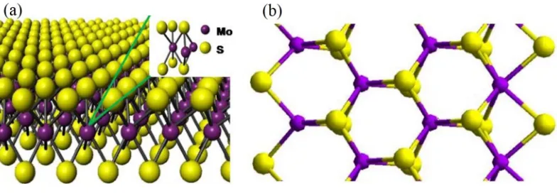
Graphene consists of a single layer of sp2 hybridised carbon atoms in a honeycomb lattice [1, 5]. A high resolution high angle annular dark eld (HAADF) scanning transmission electron microscope (STEM) image of the hexagonal structure is shown in gure 2.1(a) [44]. Graphene exhibits supremacy in mechanical properties (Young's modulus of 1 TPa, intrinsic strength of 130 GPa), charge-carrier mobility (2.5 cm2 V−1 s−1), sustainable electric current density (a million times higher than copper) and thermal conductivity (above 3,000 WmK) [1, 6, 4649].
transmit-(a) (b) (c)
Figure 2.1: Graphene lattice and 2D band generation from transition sliding. (a) is a high resolution HAADF STEM image from Pan et al. [44]. (b) shows a reference transition (constructed symmetrically about the Dirac point) where absorption is followed by emission along the reverse path producing a net total of two phonons of opposite momentum. (c) shows a sliding transition (moved up in this case) which still ts absorption and emission transitions along the Dirac cone. The reference transition is shown as a dashed rectangle. Sliding the rectangle up or down leaves the phonon 2q− unchanged and provides a continuum of transitions along the Dirac
2.1 - Graphene
tance and low sheet resistance (displacing the rare and expensive indium tin oxide (ITO)) [6, 51, 52]; as an interconnect in integrated circuits due to its excellent electri-cal and thermal conductivity; and as a barrier for DNA sequencing and water desali-nation when perforated with appropriately sized nanopores [53, 54]. The expectation that graphene-based materials may give rise to new, as yet unknown applications, is also extensive [6]. However, this diverse range of applications will require a range of synthesis and treatment techniques, which negotiate the compromises of quality and cost eciency. Novoselov et al. divided these proposed applications by the quality and other suitability factors of the required graphene material: (1) graphene or re-duced graphene oxide akes for composite materials, conductive paints, and so on; (2) planar graphene for lower-performance active and non-active devices; and (3) planar graphene for high-performance electronic devices [6].
Mechanical exfoliation, which uses for instance the scotch-tape method, produces graphene of exceedingly high crystal quality from highly oriented pyrolitic graphite (HOPG). However, it is not suitable for applications besides research due to scal-ability issues including poor control of the layer number. Liquid phase exfoliation uses a solvent and sonication to separate layers from suitable bulk materials. The graphene produced satises the requirements of the above-dened type 1 graphene applications only as it lacks precise layer control and solvents can only be removed at great diculty and cost, although oering huge scalability [55, 56]. Chemical vapour deposition (CVD) growth of graphene is highly scalable [5759] and provides graphene which satises the requirements for type 2 graphene applications (there is a greater number of defects in CVD produced material) [60]. Growth on SiC is the method which appears most applicable to type 3 graphene applications due to its relative scalability (compared to mechanical exfoliation at least though still limited to the size of the substrate) and crystal quality. However it remains distant from integration with existing technology because of several features including the high temperature required for growth, imprecise layer control, particularly at substrate terraces, and more [6, 61].
Figure 2.2: The calculated phonon dispersion relation of graphene [62, 63]. The iLO, iTO, oTO, iLA, iTA and oTA phonon branches are shown.
integrate graphene in this way, enhancing devices using relatively small changes to existing fabrication methods. However, synthesis is only a part of what is possible with huge scope left for post-synthesis modication methods as will be discussed in chapter 3 and is the main subject of this thesis.
The Raman spectra of carbon materials, including amorphous carbon, graphite, nanotubes and graphene, have been studied extensively allowing a wealth of infor-mation to be inferred including crystalite size, defect density, doping states, layer number and orientation [6368]. The unit cell of monolayer graphene contains two carbon atoms and thus six phonon dispersion bands assigned to LO, iTO, oTO, LA, iTA, and oTA phonon modes as shown in gure 2.2. According to predictions using group theory, the LO and iTO phonon modes belong to the two-dimensional E2д representation and are therefore Raman active modes [69, 70].
Experiments nd the following prominent characteristic peaks in high quality monolayer graphene spectra using laser excitation at 514 nm: 2D at∼2700 cm−1 and
2.1 - Graphene
Figure 2.3: Double and triple resonance in Raman spectra of graphene. (Left) rst-orderG band process and (center) one-phonon second-order double-resonance process for the D band (intervalley process) (top) and for the D0 band (intravalley process)
(bottom). (Right) two-phonon second-order resonance Raman spectral processes (top) for the double-resonanceG0 process, and (bottom) for the triple resonance G0
band process triple resonance (TR) for monolayer graphene [68]. For one-phonon, second-order transitions, one of the two scattering events is an elastic scattering event. Resonance points are shown as open circles near the K point (left) and the K0point (right) [63].
to normal Raman selection rules also allows the detection of two further peaks: D
at ∼1350 cm−1, and D0 (sometimes referred to as GS [45, 63]) at ∼1600 cm−1. The 2D and D bands originate from a second-order process, involving two iTO phonons near the K point for the 2D band or one iTO phonon and one defect in the case of the D band. The origin and the dispersive behaviour in the frequency of the D and 2D bands are explained using a double-resonance model (a fourth-order perturbative Raman model used in carbon materials). In this double-resonance process, the wave-vectors (q) of the phonons associated with the D and 2D bands (measured from the K point) would couple preferentially to the electronic states with wave-vectors (k) (measured from the K point), such that q≈ 2k [63].
begins with an electron of wave-vector k around K absorbing a photon of energy Elaser. The electron is inelastically scattered by a phonon or a defect of wave-vector q and energyEphonon to a point belonging to a circle around the K0point, with wave-vector k+q, where the K0 point is related to K by time reversal symmetry. The
electron is then scattered back to a k state, and emits a photon by recombining with a hole at a k state. In the case of the D band, the two scattering processes consist of one elastic scattering event by defects of the crystal and one inelastic scattering event by emitting or absorbing a phonon [63].
In the case of the G0 band, both processes are inelastic scattering events and
two phonons are involved. This double-resonance mechanism is called an inter-valley process because it connects points in circles around inequivalent K and K0 points
in the rst Brillouin zone of graphene. On the other hand, the double-resonance process responsible for the D0 band is an intra-valley process, since it connects two
points belonging to the same circle around the K point (or the K0 point) [63].
The underlying explanation for the Raman spectrum of monolayer graphene is still a subject of debate as it has also been explained using Kramers-Heisenberg-Dirac (KHD) theory which can be derived using a rst order perturbation theory approach. It describes the scattering of a photon by an electron. The KHD theory and its recent application in the case of graphene has led to the proposal of an eect labelled "transition sliding" which can occur in materials such as graphene whose electron transport properties are decribed by a Dirac cone. Transition sliding may be the process behind the very high brightness of the 2D overtone [45]. It is not clear if the KHD approach is applicable beyond a monolayer of graphene. This is illustrated in gures 2.1(b) and 2.1(c).
In graphene, the defect yield and the nature of defects introduced by these ion species are inferred from Raman spectra using established models [26, 27, 71, 72].
LD in graphene has been related to the ratio of the intensity of the D peak (ID) to the intensity of theG peak (IG) by Lucchese et al. [26] and a version is given here by:
ID
IG =CA
(L2S+2rSLS)
(L2S +2rSLS −rS2)
h
e−πrS2/L2D −e−π(L2S+2rSLS)/L2Di +C
S
h
1−e−πr2S/L 2 D
i
(2.1)
2.1 - Graphene
represent the average radii of two circular areas centred at the ion impact points. The inner and structurally disordered area caused by an ion (labelled S) is described by the radius rS. Outside of rS the lattice structure is preserved but is activated with respect to the Raman D band (within the area labelled A). The distance from the centre of the impact site to the edge of the area A is labelled rA. In other terms, a photoexcited electron-hole pair will be aected by the structural defect if the excitation process takes place in a region suciently close to the defect site i.e. a photoexcited electronhole pair must reach the defective site during the time in-terval in which the Raman process occurs. Therefore, the dierence, rA - rS should be related to the correlation length of photo-excited electrons participating in the double-resonance mechanism giving rise to the D band. LS = rA−rS is the Raman relaxation length for the resonant Raman scattering. These distances are illustrated clearly in gure 2.4(a).
Lucchese et al. used stochastic simulations to implement the model by simulating the structural evolution of a graphene sheet under ion bombardment. They randomly choose a sequence of impact positions and dened the following set of rules for each event: (1) pristine regions may turn into S or A regions, depending on the proximity to the impact point; (2) Similarly, A-regions may turn into S; (3) S-regions always remain S. Then, the initially pristine sheet evolves, as the number of impacts increase, to be mostly activated, leading to an increase of theD band. In sequence, the mostly structurally-disordered regions become increasingly widespread, leading to a decrease of the D band. The intensity of the D peak is proportional to the total S areas of crystalline graphene that area activated by local defects, not the areas of the defects themselves. Thus, as LD becomes suciently low and the material becomes less crystalline, the D band intensity falls. This is illustrated in the overlapping defect regions in gure 2.4(b).
The dispersive eect of the excitation energy,El, on the ratio of excitation of the
(a) (b)
Figure 2.4: D band generation from regions adjacent to defect sites [26]. (a) shows the distances from the impact point of the ion to the edge of the A (rA) and S (rS) areas from Lucchese et al. [26]. (b) from Pan et al. shows the inter-defect distance (LD) and the overlap between defect-activated regions typical in the highly disordered range [44].
[73]. Where El is stated in eV,CA has been given experimentally by: [27]
CA= (160±48) ×El−4 (2.2)
TheCS parameter is the value of theID/IG ratio in the highly disordered limit and it is important only in the large defect density regime, LD ≤ rS [26, 27]. Typically, three stages are discussed in the evolution of the relationship described by equation 2.1. The rst stage begins with pristine graphene (having a very large LD) and as disorder is increased, a risingD peak may be observed, increasingID/IG. In addition, a broadening of all peaks occurs. It can be attributed to isolated defects initially appearing in a crystalline lattice. The second stage features a now diminishing D
2.2 - Molybdenum Disulphide
specimen to amorphous carbon bearing limited or no resemblance to the original graphene.
Monolayer graphene has several clear factors distinguishing its Raman spectrum from those of bilayer and few layer graphene. Monolayer graphene has a single, sharp 2D peak, roughly four times more intense than the G peak (this can be less in the case of defective monolayer graphene, still distingusihed by being greater than twice as intense as the G peak) [65]. By comparison, the 2D band of bilayer graphene is upshifted, much broader and has four components. For more than ve layers the Raman spectrum becomes hardly distinguishable from that of bulk graphite. The 2D peak in bulk graphite consists of two components 2D1 and 2D2, roughly a 1/4 and 1/2 the height of the G peak respectively. This evolution of the 2D peak as a function of graphene layer number is shown in gure 2.5. There are other eects of layer number on the G peak which are weaker indicators of layer number. The G
band is shifted downward in frequency with increasing layer number but this is a very weak trend beyond bilayer graphene [64, 75].
The alteration of graphene by irradiation techniques has received much focus recently and is built upon in this work [26, 27, 29, 74]. Combining the Raman spectrum of graphene and equations 2.1 and 2.2 with a precise method for the intro-duction of defects allows the powerful manipulation of graphene's properties through defect-engineering. The model is so detailed that both the defect type and density can be distinguished. This will be demonstrated experimentally for supported and freestanding graphene irradiated with He+ and Ne+ in chapter 5.
2.2 Molybdenum Disulphide
(a) (b)
2.2 - Molybdenum Disulphide
hexagonal rings (see gure 2.7) and has a thickness of∼0.7 nm [20]. Unlike graphene, monolayer MoS2 has a sizeable direct band gap of 1.8 eV. Interestingly, MoS2 has an indirect band gap in the multi-layer system and a direct band gap in the monolayer [12, 78]. This suggests potential for application in digital electronics and numerous photonic applications such as light emitters, photodetectors and solar cells [79, 80]. Excellent mechanical exibility also allows potential for use in exible electronics [81].
The eects of strain and substrate [82, 83] and optical control [84] on the pho-toluminescence spectroscopy (PL) spectrum of MoS2 have been reported. In the monolayer form, MoS2 has a large direct band gap with intense emission [9, 10]. This intensity declines rapidly with increasing layer number. Figure 2.6(a) shows the calculated band structures of monolayer and bilayer MoS2. Electronic states near the Γ point arise from orbitals with strong interlayer coupling and depend on layer number. However, conduction band states at the K point are in orbitals in the middle of the layer and because of this are independent of interlayer coupling [85, 86]. This coupling can also be reduced by folding which leads to an enhancement of the photoluminescence emission yield [86].
The method by which MoS2 is synthesised is a major factor in its intrinsic de-fect density and type, its crystal size and the layer number [89]. Monolayer MoS2 produced by mechanical exfoliation from bulk is widely regarded as the nest qual-ity available. Monolayer MoS2 produced by CVD instead can have reduced charge carrier mobility by around an order of magnitude in devices [90]. MoS2 displays native n-type doping. Sulphur vacancies exist, even in high quality samples and these introduce localised donor states inside the band gap [91, 92]. Achieving p-type doping is much sought after and has been acheived by low energy phosphorus implantation [25], molybdenum oxide heterojunctions [93, 94] and partial oxidation [95, 96] amongst other techniques. However, none of these methods demonstrate the high control, spatial resolution and scalability that would be required for commerical purposes.
(a) (b)
Figure 2.6: The Brillouin zone and band structure of MoS2. (a) shows the band structure of monolayer (top) and bilayer (bottom) calculated by DFTMoS2 [87]. (b) shows the rst Brillouin zone of MoS2 [88]
[image:44.612.129.521.462.598.2]2.2 - Molybdenum Disulphide
modes in bulk MoS2 [98] (of polytype 2H, point group D6H) corresponding to the following symmetries (wavenumbers for 514 nm excitation): E2
2д (35 cm
−1),E
1д (286 cm−1),E1
2д (383 cm
−1) andA
1д (408 cm−1). Other modes are expected to be infrared (IR)-active or silent [101].
In monolayer MoS2 (of polytype 1H, point group D3H), the phonon dispersion has been well described theoretically and computationally using DFT [109]. The results are in good agreement with experiment [101, 106, 109]. The bulk phonon dispersion of monolayer MoS2 has three acoustic modes. The longitudinal acoustic (LA) and transverse acoustic (TA) modes vibrate in-plane, have a linear dispersion and a higher energy than the out-of-plane acoustic (ZA) mode which has aq2 depen-dence [109]. TheLA(M)peak at∼227 cm−1 has been linked to the presence of a local maximum in the vibrational density of states, located at the energy corresponding to the longitudinal acoustic (LA) branch at the edge of the Brillouin zone. It ex-hibits no intensity in pristine monolayer MoS2 but intensies quickly with increased defect density [28, 103]. It is typically very weak and somewhat broad. It is also found in nanoparticle/few layer samples. Since it is defect-activated, it can be used somewhat analogously to the D band in graphene Raman spectra in the characteri-sation of defect density [28]. In resonance Raman spectroscopy, for a variety of MoS2 arrangements the LA(M) mode is notable for its many second order interactions in spectra.
The high energy optical modes that are Raman active in monolayer MoS2 are the following: the E0peak at ∼385 cm−1 arises from the intralayer, in plane motion of Mo and S atoms with respect to each other and theA0
1 peak at ∼405 cm
−1 arises from the intralayer, out of plane motion of S atoms. Both the E0and theA0
1 peaks are strong in all forms of MoS2
(a) (b)
Figure 2.8: Vibrational modes and Raman spectroscopy for the dierentiation of the number of MoS2 layers thinned by plasma [12, 13]. (a) shows the vibrational modes giving rise to both peaks in the part of the Raman spectra shown in (b).
E0 and A0
1 peaks [110]. Peak separation is a key characteristic in distinguishing layer numbers [12, 106, 111, 112]. Figure 2.8 shows the evolution of Raman spectra extracted from 1-4L MoS2. With increasing layer number, a characteristic red shift of the E0/E1
2д (385 cm
−1 to 382 cm−1) and blue shift of the A0
1/A1д (404 cm
−1 to 407 cm−1) modes is observed. With increasing sample thickness, a classical model for coupled harmonic oscillators would suggest that both peaks would blue shift. However, this is a simplistic view for 2D materials [13]. While the A1д vibration does blue shift,the E1
2д vibration in fact red shifts, possibly the result of surface relaxation and additional interlayer interactions for few-layer samples [1113]. For four or more layers, the values of frequency converge to bulk values. With regard to the width of the observed peaks, theE0/E1
2д peak is largely independent of thickness. It has been reported that the width of theA0
1/A1д peak drops going from 2 to 6 layers but it remains dicult to use this to distinguish between layer numbers [11, 106].
The evolution of the Raman spectra of monolayer MoS2 with decreasing LD has been described by Mignuzzi et al. as follows: The intensity of theLA(M)peak,I(LA), normalized to that of either the E0 peak, I(LA)
I(E0), or the A01 peak, I
(LA)
I(A0
2.2 - Molybdenum Disulphide
the inverse square ofLD (as with graphene, the average distance between defects) by equation 2.3 [28]:
I(LA)
I(X) =
C(X)
L2 D
(2.3)
In the case where the Raman spectrum was acquired with a 532 nm laser, the fol-lowing constants were found by tting experimental data: C(E0) = 1.11±0.08 nm2 andC(A01)=0.59±0.03nm2. X = E0orA01 for depending on the peak studied. With rising disorder, the increase of these intensity ratios is attributed to two concomitant factors: (i) an increase in the absolute intensity of the defect-activated LA(M) peak, and (ii) a decrease in the intensity of the E0 and A0
Chapter 3
Modication Methodology
I
n chapter 2, the two key materials of this work were identied, namely graphene and MoS2, and some of their extraordinary properties were described. In this chapter, the eld of nanomaterial engineering will be introduced and the modication methods which dominate this work will be highlighted. The primary method used in this work for the modication of 2D materials is by the application of an energetic ion beam in an ion microscope which is capable of nanoscale resolution. These ion microscopes as ion sources will be briey described and there will be an exploration of the ion-beam sample interaction. Methods for simulating ion beam interactions such as molecular dynamics and Stopping and Range of Ions in Matter software (SRIM) are also introduced and discussed.Another modication method uses a high energy electron beam in a scanning electron microscope (SEM) to excite gas atoms for reactions with a surface. Finally, the alteration of MoS2 by oxidation in air is discussed in detail, as it will be shown to be highly controllable through the use of ion irradiation.
3.1 Nanomaterial Engineering
of 10s of nanometres) and throughput. At present, scalable modication is often achieved by a wide variety of methods including defect-engineering in synthesis, or with plasma or ion implantation, doping by a range of techniques including chemical reactions and ion irradiation, encasement in other materials to create heterostruc-tures and more. While chemical reactions and plasma etching can have a great deal of control over properties, they are typically unable to do so with much spatial speci-city. It has been shown previously in experiments and simulations that ion and electron irradiation can selectively etch or alter the properties of selected regions of 2D materials with high spatial resolution [37, 41, 113116]. Sputtering is the removal of near-surface atoms from a target, and the sputtering yield is the mean number of sputtered target atoms per incident electron/ion. Broadly speaking, electron beams can achieve atomic or near-atomic resolution but with a throughput much lower than that of ion beam techniques due to their lower sputtering yield. Ion beam methods can still achieve several nanometre resolution at a fraction of the cost/time.
Considerable alteration of 2D materials is possible by tailoring the crystal struc-ture/defect density, layer number, stoichiometry/doping state and geom-etry including polytypes and nanostructures like pores and nanoribbons. Defects have been introduced to MoS2 on a large scale during CVD with extensive control over the resulting electrical properties [20, 90]. DFT simulations have demonstrated that the modication of crystal structure by the controlled addition of defects can be used to tune the electronic structure and transport properties of MoS2 [117]. While electron transport is practically isotropic in pristine MoS2, strong anisotropy is observed in the presence of defects. Localised midgap states are observed in semi-conducting MoS2 that do not contribute to the conductivity but scatter the current with direction-dependency.
3.2 - Ion Beams
Devices fabricated from MoS2monolayers with lower sulphur in their stoichiom-etry have negligible current-voltage hysteresis and a threshold voltage of ∼0 V [119]. Alteration of the geometry of MoS2 can also result in modied electrical and mag-netic behaviour [22]. It will be shown in this thesis that all of these characteristics can be altered to some extent using ion irradiation.
With regard to geometry, nanoribbons are particularly desired. These strips of extremely thin and narrow material (typically dened as having a width of less than 100 nm), can have superlative properties especially with pristine crystallinity and edges of a specied orientation (i.e. zigzag, armchair) [120]. Simulations show that MoS2 nanoribbons with such edge orientations and widths of ∼3 nm (within the quantum connement regime) can be vastly dierent in behaviour depending on the edge termination. For example, zigzag MoS2 nanoribbons are ferromagnetic and half-metallic whereas armchair MoS2 nanoribbons are non-magnetic and semi-conducting [17, 22, 121]. Of the many methods used to fabricate nanoribbons in MoS2, few have achieved all of the following: good crystal structure, well-dened edges, reproducibility and widths of less than 10 nm [30, 31]. Electron irradiation in a TEM has been used to fabricate ribbons of MoS2 down to sub-nanometre widths [33]. However, the TEM is a low throughput fabrication tool due to a relatively weak beam-sample interaction and stringent sample requirements (supported, thin, low levels of contaminants, vacuum stable). Similarly, nanoribbons of graphene have been fabricated using scanning probe microscope-based lithography, but again issues of throughput and controllability persist [122124].
3.2 Ion Beams
The conventional FIB has been commonplace for several decades and uses a liquid metal ion source (LMIS) to accelerate gallium ions (Ga+) to energies in the typical
range of 1-30 keV. In operation, Ga+ is focused into a ne probe, which on modern
instruments can be small enough to obtain image resolutions in the 3 to 5 nm range [125]. Due to the energy and large mass of Ga+, there is a very strong sample
(a) (b) (c)
Figure 3.1: The GFIS in the GIM. (a) A schematic view of a GFIS [127]. (b) Imaging a trimer in SFIM mode in a Gas Field Ion Source microscope [126]. (c) Schematic of a GFIS microscope [126].
[125]. Thus, many of the uses of aGa+ ion beam are related to micromachining and
nanofabrication rather than imaging [126].
The gas ion microscope (GIM) is a more recent development with very dierent underlying physics governing its ion source [126, 128, 129]. One such tool is the Zeiss ORION series of microscopes such as the Zeiss ORION Plus (He+) and Zeiss ORION
Nanofab (He+ or Ne+) utilised in this work. The ORION Nanofab is equipped for
3.3 - Ion Beam Sample Interaction
As in SEM and FIB, images are formed in the Nanofab microscope by detecting secondary electrons generated by the primary beam. However, these images present dierent information than in SEM. This is because of the dierent nature of the ion beam-sample interaction and resultant signicantly smaller penetration depth of ions compared to electrons. Images acquired using He+ are much more surface sensitive
than energetically equal electrons [113]. It is found that in imaging applications and using He+, the GIM can outperform the SEM, given its smaller interaction
range (hundreds of nm compared to µm) and probe size (0.35 nm compared to∼0.8 nm for a world class SEM) [126, 128130]. Due to the relatively low mass of He+
compared to other available accelerated ions it has a lesser ability to sputter material when compared to either Ne+ orGa+ at the same angle and energy. However, its
interaction at the specimen surface is still far greater than that of an electron beam of equal current. Given its much higher mass, Ne+ has an enhanced calculated milling
capability compared to He+ (at least an order of magnitude for copper at an energy
of 20 keV) [129].
Due to the very high brightness of the GFIS source, the attainable probe size of 0.3-0.5 nm in He+ mode is much smaller than that of Ga+ in the FIB. Potential
resolution of theNe+ mode when further developed is also suggested to be as low as
sub-nanometre [129]. However, in practice the current achievable probe size of Ne+
is approximately 2.5-5 nm which is similar to Ga+.
3.3 Ion Beam Sample Interaction
Ion irradiation has an illustrious record over many decades in the scalable, pre-cise engineering of materials [23]. Given the pivotal importance of defect-engineering and nanofabrication methods in the materials science of today, it is imperative that the capabilities and side-eects of ion beam fabrication methods on 2D materials be well understood. The ion species and energies used in this work are particularly signicant due to their high resolution capability for nanofabrication and defect-engineering.
As a beam of ions reaches the specimen, collisions with the surface will transfer energy to the sample. The maximum transferable energy from an ion to a specimen atom by elastic scattering (modelling the atom and ion as two spheres, reasonable given the high energies involved),Tm, depends on the particle energy, E, and the ratio of the ion mass, M2, to the specimen atom mass, M1 [23], where:
Tm = 4M1M2
(M1+M2)2E (3.1)
An ion interaction leading to the removal of a specimen atom has a cross-section
σd(ion). This is given in equation 3.2 wheree is the charge of an electron,Z1 and Z2 are the atomic numbers of the specimen atoms and beam ions respectively, andTD is the threshold displacement energy of the specimen atom, such that [23]:
σd(ion) =π
M1
M2
Z2 1Z22e4
1
E
1
TD − 1
Tm
(3.2)
3.4 Simulating Ion Interactions
SRIM is a software package, which is used to model the interaction of ions with matter. The trajectory and penetration depth of an ion beam can be simulated in a specimen surface with a variety of inputs including ion species and energy and the specimen composition [131]. SRIM is based on a Monte Carlo simulation method, namely the binary collision approximation. In calculating the sputtering yield of atoms from a supported 2D material, SRIM accounts for: those atoms directly re-moved by the primary ion beam, those which are rere-moved by backscattered primary ions and those which are removed by secondary atoms, excited in the substrate near the surface. It is a singularly useful tool for comparing the eects of ion energy and species on the milling and patterning of materials. Figure 3.2 shows a comparison of the trajectories of He+,Ne+ andGa+ into a 4 nm layer of MoS
2 on a substrate of magnesium oxide (MgO) calculated using SRIM.
3.5 - Dose and Substrate Eects
Figure 3.2: A Stopping and Range of Ions in Matter software simulation of ion trajectories. The gure shows a calculation for 30 keV He+, Ne+ and Ga+ beams
incident on a 4 nm layer of MoS2 sitting on a substrate of MgO.
are neglected. The amorphous structure assumed here is also highly inapplicable to measurements of 2D materials due their typically highly ordered lattices and their 2D nature.
Therefore, molecular dynamics and DFT are in many cases a superior choice where accuracy in 2D material systems is concerned. However both are far more computationally expensive choices with DFT being particularly so [28, 34, 132135]. While SRIM and molecular dynamics methods do not distinguish between the eects of atoms and ions (chemical eects) these are expected to be negligible in this work given the high energies of the direct ion beam. Where possible, values calculated from molecular dynamics in the literature are referred to rather than SRIM.
3.5 Dose and Substrate Eects
material is unavoidable. Excessive doses are undesirable due to the way in which they exacerbate this eect while also reducing fabrication throughput. In addition, the resolution of long exposures may be subject to drift of the sample with respect to the beam. Since modelling and reducing the impact of undesired damage will be one of the challenges of this work, optimising the irradiation dose for complete milling is of great importance. As an example, the dose required to remove a layer of supported MoS2will be estimated. Since the area of the MoS2 unit cell (a = 0.31625 nm) is ∼0.14 nm2, there are 1.5 × 1015 cm−2 sulphur atoms and 7.3 × 1014 cm−2 molybdenum atoms. An estimate for the dose of ions,D, required to remove a given area is given by
D =N/P (3.3)
where N is the total number atoms per unit area and P is the average probability of removing an atom. Here we use the sputtering yield as calculated from SRIM simulations (see section 3.4) for He+ at 30 keV, P = 0.03. This method ignores the
distribution of such atoms and will thus underestimate the true dose. The eects of ion beam-induced deposition will also cause an underestimation. However, the value of D obtained is of the order 1 × 1017 cm−2 which has been found in preliminary experiments to be correct to within an order of magnitude, see chapter 6.
3.6 - Displacement Threshold in MoS2
Figure 3.3: Displacement cross sections of atoms in MoS2 with 30 keV He+. Mo atoms are shown in purple and S atoms are shown in yellow. The size of the circles shown in dotted lines represents the sputtering cross sections of the respective atoms.
supported graphene (on a substrate of SiO2) were 5 keV and 3 keV forAr+ (M=18) and Si+ (M=14) respectively [136].
3.6 Displacement Threshold in MoS
2Most experimental studies of the sputtering of MoS2note that S atoms are sputtered preferentially. Since they also make up two thirds of the total atoms and there are no Mo-Mo bonds in pristine MoS2, it is reasonable to say that to remove all material (from a freestanding sample at least) it is essentially necessary only to directly remove the S atoms. For that reason, the removal of S atoms will be explored in some detail. The displacement threshold of an S atom is a major factor in deciding the probability of sputtering as in equation (3.2), see gure 3.3.
Within a sample of MoS2 there are many factors aecting the displacement threshold value. The rst is that assuming a 0◦ angle of incidence in MoS
site. In tungsten disulphide (WS2) the displacement energy for S atoms at the edge is 4.2 eV compared to 7.0 eV away from the edge1 [115].
3.7 Ion Beams and 2D Materials
With the demands of modern semiconductor technology, precise nanoscale control of 2D material properties is much sought after and eminently achievable using modern ion irradiation techniques with sub-nanometre probe sizes [3540, 113]. Given the superlative connement of such materials, it is possible to restrict the ion-induced eects to an exceptionally small region. Such methods have been used to create nanoribbons with widths of less than 10 nm [36, 37, 137], control doping of graphene by implantation [25] and introduce precise quantities of defects [2729]. Ribbon widths of this magnitude may be useful in order to exploit the properties of quantum connement. However, nanoribbons must also have well-dened edge orientations and good crystallinity which are limited by a shortfall in our understanding and subsequent control of the beam-sample interaction. Whether this can be achieved by
He+ milling has not yet been reported and fabricated edges have been insuciently
studied to date by methods of sucient resolution. Eects of the same scanning strategies varied across materials have also not been investigated to any meaningful extent.
More nuanced and innovative uses are also possible than simple direct write milling. He+ irradiation of graphene encapsulated in hexagonal boron nitride has
even been used to introduce n-type doping [41]. Defect-engineering is also readily achievable with a great deal of both precision and spatial resolution. A host of optical, mechanical and electronic properties can be controlled in this way, by using the He+ beam to create vacancies [138].
In short, the further development of irradiation methods for a given material is predicated on a thorough understanding of the relationship between irradiation strategy and dose and the corresponding rate of defect introduction and the nature and size of defects. The spatial spread of beam-induced eects is also of paramount
3.8 - Electron Beams and Defects
importance, limiting the ultimate minimum feature size, of critical importance to nanofabrication.
3.8 Electron Beams and Defects
Another modication method used in this work is the etching of graphene in a SEM using nitrogen activated by the electron beam. While the SEM has been shown to be capable of selective deposition and removal of material, an electron beam of typical energy in a SEM (<30 keV) is not energetic enough to eciently sputter carbon atoms. However etching is quickly and eciently achieved by other methods including the introduction of a gas into the system [139142]. The electron beam is used to generate reactive ions which locally etch the sample surface in close proximity to spots dened by the microscope [140, 141, 143]. This technique provides direct, top-down fabrication of nanostructures using a maskless and resistless process. Of particular interest is the ability to create nanopores in graphene.
Oxygen is the most commonly used gas as the etching species. State of the art e-beam etching was recently demonstrated with water vapour, producing feature sizes down to 7 nm [142]. Etching of a graphene surface has previously been observed to occur when it was irradiated with an electron beam in a nitrogen atmosphere [143]. In chapter 5 nitrogen gas is shown to be preferable to oxygen as it reacts less aggressively with the graphene, allowing smaller feature sizes, down to 4.5 nm, to be demonstrated compared to other methods.
3.9 Oxidation of FLM-MoS
2in the Literature
molybdenum trioxide (MoO3) and sulphur dioxide (SO2) molecules, respectively.
MoS2(s)+3.5O2(д) → MoO3(s/д)+2SO2(д) (3.4)
The temperature at which the reaction occurs depends greatly on the condition of the material with pulverised MoS2 having oxygen content at temperatures as low as 100◦C and some coatings being stable up to 400 ◦C [144, 147]. The case of the
oxidative reaction of few layer or monolayer (FLM)-MoS2 is of far greater inter-est to the modern nanomaterials scientist and has been developed to a far lesser extent due to the relatively recent proliferation of the material. Yet, the implica-tions for applicaimplica-tions under the categories of device fabrication, stability and defect-engineering/doping are profound. FLM-MoS2 is much more reactive to molecular oxygen (O2) than an analogous atomic membrane of graphene [148]. It has recently become clear that chemical oxidation occurs preferentially at edges and defect sites [148, 149].
Oxidation has been demonstrated to alter the doping state and performance of FLM-MoS2 devices and to thin or even completely etch FLM-MoS2 [20, 95, 148]. McDonnell et al. demonstrated MoOx as an ecient hole injection layer for p-type eld eect transistors (FETs) in TMDs [94]. It is well-established that the oxidative thinning and/or etching of FLM-MoS2 can be achieved by heating in the presence of O2 or other oxidants [95, 118, 148, 150, 151]. However, there remains a great deal of room for expanding on this knowledge. For instance, the behaviour of MoO3 as a reaction product is complex due to its volatility. Whether it sublimes or at least partially remains after the oxidation of FLM-MoS2 seems to be heavily dependent on the thickness of the starting material [148]. However, there appears to be no proposed mechanism for this phenomenon.
![Figure 2.4: D band generation from regions adjacent to defect sites [26]. (a) showsthe distances from the impact point of the ion to the edge of the A (rA) and S (rS)areas from Lucchese et al](https://thumb-us.123doks.com/thumbv2/123dok_us/1491746.689467/40.612.178.472.101.285/figure-generation-regions-adjacent-showsthe-distances-impact-lucchese.webp)
![Figure 2.5: Evolution of the 2D peak as a function of number of layers [65]. 2.5(a)shows the 2D peak in the Raman spectrum of monolayer graphene and bulk graphite.2.5(b) shows changes to the band as layer number changes for both 514 and 633 nmexcitations.](https://thumb-us.123doks.com/thumbv2/123dok_us/1491746.689467/42.612.119.534.232.483/evolution-function-spectrum-monolayer-graphene-graphite-changes-nmexcitations.webp)

![Figure 3.1: The GFIS in the GIM. (a) A schematic view of a GFIS [127]. (b) Imaginga trimer in SFIM mode in a Gas Field Ion Source microscope [126]](https://thumb-us.123doks.com/thumbv2/123dok_us/1491746.689467/52.612.112.537.105.275/figure-gfis-schematic-imaginga-trimer-field-source-microscope.webp)
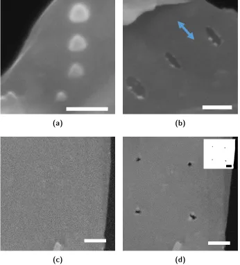
![Figure 3.4: Thermal thinning and etching of 2L MoS2 nanosheets. Wu et al. showedthermal thinning (a),(b), and etching (c),(d), of 2L MoS2 nanosheets to 1L MoS2at 330◦C for 10 h [95]](https://thumb-us.123doks.com/thumbv2/123dok_us/1491746.689467/63.612.74.500.215.460/figure-thermal-thinning-nanosheets-showedthermal-thinning-etching-nanosheets.webp)

![Figure 4.1: Jablonski diagram illustrating Stokes and anti-Stokes shifts [164].](https://thumb-us.123doks.com/thumbv2/123dok_us/1491746.689467/70.612.127.525.100.252/figure-jablonski-diagram-illustrating-stokes-anti-stokes-shifts.webp)
![Figure 4.5: Outline of a transmission electron microscope (left) and a scanning trans-mission electron microscope (right) [184].](https://thumb-us.123doks.com/thumbv2/123dok_us/1491746.689467/80.612.184.464.383.621/figure-outline-transmission-electron-microscope-scanning-electron-microscope.webp)