Search for alternative magnetic tunnel junctions based on all-Heusler stacks
Worasak Rotjanapittayakul,1Jariyanee Prasongkit,2,3Ivan Rungger,4,5Stefano Sanvito,4Wanchai Pijitrojana,1and Thomas Archer4,*
1Department of Electrical and Computer Engineering, Faculty of Engineering, Thammasat University, Bangkok, 10120, Thailand 2Division of Physics, Faculty of Science, Nakhon Phanom University, Nakhon Phanom, 48000, Thailand
3Thailand Center of Excellence in Physics, Commission on Higher Education, 328 Si Ayutthaya Road, Bangkok, 10400, Thailand 4School of Physics and Centre for Research on Adaptive Nanostructures and Nanodevices, Trinity College Dublin, Dublin 2, Ireland
5Materials Division, National Physical Laboratory, Teddington, TW11 0LW, United Kingdom
(Received 17 February 2016; revised manuscript received 21 May 2018; published 23 August 2018)
By imposing the constraints of structural compatibility, stability, and a large tunneling magneto-resistance, we have identified the Fe3Al/BiF3/Fe3Al stack as a possible alternative to the well-established FeCoB/MgO/FeCoB
in the search for a novel materials platform for high-performance magnetic tunnel junctions. Various geometries of the Fe3Al/BiF3/Fe3Al structure have been analyzed, demonstrating that a barrier of less than 2 nm yields
a tunneling magneto-resistance in excess of 25 000% at low bias, without the need for the electrodes to be half-metallic. Importantly, the presence of a significant spin gap in Fe3Al for states with1symmetry along the
stack direction makes the TMR very resilient to high voltages.
DOI:10.1103/PhysRevB.98.054425
I. INTRODUCTION
Spin valves displaying large tunnel magneto-resistance (TMR) have undoubtedly revolutionized the electronics in-dustry and now form the central component of many tech-nologies, the most successful device being the read heads in hard-disk drives [1]. Importantly, spin valves are set to become the central component of many devices of the future, such as magnetic random access memories and spin-torque oscillators. The major breakthrough was the fabrication of epitaxial CoFeB/MgO/CoFeB spin valves [2,3], which exploit coherent electronic tunneling [4,5] to provide a large TMR even at room temperature. In practical devices the fabrication of CoFeB/MgO/CoFeB spin valves requires the growth of rather complex thin films stacks, including functional layers (e.g., for magnetic pinning) and seed layers necessary for the epitaxial growth. It is then desirable to enlarge the available materials platform beyond the CoFeB/MgO system. However, despite a large effort in both industry and academia [6], no junction alternative to CoFeB/MgO/CoFeB has been adopted by the community. This is a significant deficiency, since little room is left for tuning the materials properties necessary for the devel-opment of new applications of the technology. It is therefore imperative to explore alternative materials combinations which offer more freedom to engineer the device properties.
Heusler alloys are a large class of binary (X3Z), ternary
(X2Y Z), and quaternary (XXY Z) compounds with more than
1500 known members and an impressively wide range of properties [7]. Many elements can be incorporated into the Heusler structure, making it rich and tunable, and as such ideal for developing new technologies.
*archert@tcd.ie
One key example for the switching of tunnel junctions is the Gilbert damping, which is strong in the FeCoB system [8], restricting the maximum operational frequency. Many Heuslers including Fe3Si [9], Co2FeSi [10], and Co2FeAl [11]
all show a significantly lower Gilbert damping in comparison to FeCoB. Unfortunately, to the best of our knowledge, the Gilbert damping of Fe3Al, our most promising alternative material, has
not been measured.
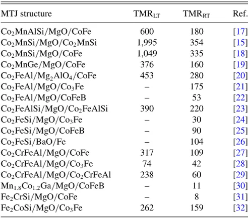
Several attempts have been made to substitute the magnetic electrodes of the FeCoB/MgO/FeCoB stack with Heusler magnets, and successes have been obtained by replacing one or both the electrodes with Co2Y Z, where Y =Fe, Mn and
Z=Si, Al [12–15]. This body of works is summarized in Table I. To the best of our knowledge, the highest TMR observed was for Co2MnSi/MgO/Co2MnSi, which displays
a TMR ratio of 1,995% at 4 K [15]. In this system, however, the magnetoresistance is sensitive to temperature with the TMR reducing to 354% at room temperature [15]. Such temperature sensitivity suggests interfacial magnetic defects or secondary phases, which disrupt the coherent tunneling. Co and Mn can directly substitute into the rock-salt MgO structure with formation energies of−3.0 eV and−4.0 eV, respectively [16], making substitutional Mn in the MgO lattice a likely culprit.
A second approach has been to construct all Heuslers giant magneto-resistance (GMR) stacks, where the spacer between the magnetic electrodes is a metal. The relevant literature is summarized in Table II. Although a MR has been demon-strated, it was found small for all the known experiments, so that further work is needed to explain these negative results in view of the large MR predicted by ab initiocalculations [33].
TABLE I. Magnetic tunnel junctions incorporating Heusler alloys electrodes reported to date. The TMR is provided for low tempera-ture (LT: 2–16 K) and room temperatempera-ture (RT:∼300 K), whenever available.
MTJ structure TMRLT TMRRT Ref.
Co2MnAlSi/MgO/CoFe 600 180 [17]
Co2MnSi/MgO/Co2MnSi 1,995 354 [15]
Co2MnSi/MgO/CoFe 1,049 335 [18]
Co2MnGe/MgO/CoFe 376 160 [19]
Co2FeAl/Mg2AlO4/CoFe 453 280 [20]
Co2FeAl/MgO/Co3Fe – 175 [21]
Co2FeAl/MgO/CoFeB – 53 [22]
Co2FeAlSi/MgO/Co2FeAlSi 390 220 [23]
Co2FeSi/MgO/Co3Fe – 30 [24]
Co2FeSi/MgO/CoFeB – 90 [25]
Co2FeSi/BaO/Fe – 104 [26]
Co2CrFeAl/MgO/CoFe 317 109 [27]
Co2CrFeAl/MgO/Co3Fe 74 42 [28]
Co2CrFeAl/MgO/Co2CrFeAl 238 60 [29]
Mn1.8Co1.2Ga/MgO/CoFeB – 11 [30]
Fe2CrSi/MgO/CoFe – 8 [31]
Fe2CoSi/MgO/Co3Fe 262 159 [32]
materials alternative to the Fe/MgO system? In this work we will use simple design concepts andab initiocalculations to screen candidates based on the symmetry filtering mechanism, which has been so successful for the Fe/MgO junction. Our analysis returns the Fe3Al/BiF3 system as a promising stack
for large magnetoresistance with a strong TMR retention at high bias. The paper is organized as follows. We open our discussion by explaining the criteria that have brought us to focus on a particular Heusler alloys stack, by looking first at the barrier and then at the magnetic electrodes. Then we move to discuss the transport properties of several Fe3Al/BiF3/Fe3Al
junctions with different barrier thicknesses. We first look at the zero-bias properties and then move to the finite-bias ones. Finally we conclude.
II. SCREENING THE MATERIALS
A. The tunnel barrier
In order to propose a new junction we must satisfy a number of constraints, which we will use to screen candidate materials combinations. First, the barrier material must be a robust insulator and therefore must have a large band gap,Eg. If we
[image:2.590.301.547.130.445.2]use a cutoff band gap of 2.5 eV, we will reduce the number of the candidate Heusler materials from over 300 000 (these include
TABLE II. All-Heusler metallic junctions grown to date. The GMR [%],RA [m·μm2] and the method (Exp.=experimental
data,ab initio=theoretical prediction) are given.
All Heusler structure GMR RA Method Ref.
Co2MnGe/Rh2CuSn/Co2MnGe 6.7 4 Exp. [34]
Co2MnSi/Ni2NiSi/Co2MnSi – 0.24 Exp. [35]
[image:2.590.38.284.683.743.2]Co2CrSi/Cu2CrAl/Co2CrSi ∼106 – ab initio [33]
TABLE III. All possible insulating Heusler materials having a wide band gap, Eg2.5 eV. The Strukturbericht (SB) symbols, lattice constant (a0[ ˚A]), band gap (Eg[eV]), tetragonal ratio (c/a0), and the method with which they have been investigated are given (Exp.=experimental data,ab initio=theoretical prediction from AFLOW.org).
Material SB a0 Eg c/a0 Method Ref.
BaBrCl C1b 7.604 3.476 – ab initio [16]
BiF3 D03 5.861 5.100 1.0 Exp. [42–44]
BrClSr C1b 7.262 4.670 – ab initio [16]
BrClPb C1b 7.251 3.090 – ab initio [16]
BrCaCl C1b 6.973 4.386 – ab initio [16]
BrHgK C1b 7.948 3.253 – ab initio [16]
Br2KLi L21 7.647 3.313 – ab initio [16]
Br2KNa L21 7.784 3.337 – ab initio [16]
Br2KTl L21 8.083 3.330 – ab initio [16]
Br2LiNa L21 7.251 3.045 – ab initio [16]
Cl2GaK L21 7.493 3.424 – ab initio [16]
Cl2GaNa L21 7.198 3.032 – ab initio [16]
Cl2InK L21 7.718 3.154 1.2 ab initio [16,42]
Cl2KLi L21 7.230 4.293 1.0 ab initio [16,42]
Cl2KNa L21 7.367 4.277 – ab initio [16]
Cl2KTl L21 7.749 3.801 – ab initio [16]
Cl2LiNa L21 6.793 4.194 – ab initio [16]
Cl2LiTl L21 7.397 3.281 1.2 ab initio [16,42]
ClHgK C1b 7.771 3.531 – ab initio [16]
ClKZn C1b 7.637 3.107 – ab initio [16]
ClHgK C1b 7.778 3.143 – ab initio [16]
LiMgN C1b 4.955 3.200 1.0 Exp. [45]
LiMgP C1b 6.005 2.430 1.0 Exp. [46]
LiNaS C1b 6.100 3.120 1.0 ab initio [47]
LiNaSe C1b 6.390 2.700 1.0 ab initio [47]
TaIrGe C1b 5.967 3.360 1.0 Exp. [48]
those reported in literature and the hypothetical ones contained in the AFLOW.org database) [16] to just 26. Notably, only four of these have been grown experimentally before; the remaining 22 are only predicted fromab initiocalculations [16]. The 26 barrier candidates are shown in TableIII. Note that the band gaps reported here are computed by density functional theory (DFT) in the generalized gradient approximation (GGA), therefore they are expected to be significantly smaller than the true quasiparticle band gap. As such ourEg2.5 eV criterion effectively selects insulators with a band gap, which is likely to be significantly larger than 2.5 eV.
Next we consider the transport properties of the tunnel barrier. In epitaxial spin valves the magnitude of the TMR is determined by the symmetry matching between the evanescent wave functions in the insulating barrier and the Bloch wave functions for majority and minority spins in the magnetic electrodes. In particular the TMR will be large if such wave-function symmetry match occurs for only one of the two spin species, i.e., if only one of the two spin species is transmitted with large probability [4,5].
TABLE IV. Insulating Heusler materials with a band gapEg
2.5 eV. The Strukturbericht (SB) symbols, lattice constant (aexp[ ˚A]), and experimental band gap (Eg [eV]) are given. In the final column we report the symmetry of the slowest decaying state along the [001] direction, as calculated in this work.
Material SB aexp Eg Symmetry
BiF3 D03[43] 5.861 [43] 5.10 [44] CB1 −VB
LiMgN C1b[45] 4.955 [45] 3.20 [45] CB5 ,VB1
LiMgP C1b[46] 6.005 [46] 2.43 [46] CB5 , VB 1
TaIrGe C1b[48] 5.967 [48] 3.36 [48] CB1 ,VB2
of self-interaction corrections drastically improve the band gap of a broad range of insulators, and here it brings the calculated gap of the chosen Heusler barriers within 10% from the experimental one. Core electrons are treated with norm-conserving relativistic Troullier-Martin pseudopotentials [39], while multi-ζ numerical atomic orbitals are used to represent the electron density and all the operators. Total energies are computed on a uniform real-space grid with an equivalent cutoff of 600 Ry, while the primitive unit cells are sampled with a 8×8×8 k-point mesh over the Brillouin zone. The linear response conductance is calculated with the DFT-based nonequilibrium Green’s functions code SMEAGOL [40,41], where the typicalk-point sampling for a given heterojunction is 100×100×1.
For each of the insulators we determine the symmetry of the slowest decaying state along the [001] direction, and we restrict ourselves to the experimentally verified insulating Heusler alloys, namely, BiF3, LiMgN, LiMgP, and TaIrGe. Our results
are presented in Table IV, where we list the experimental structural parameters and quasiparticle band gap, together with the symmetry of the evanescent wave function with the slowest decay across the barrier. Notably, while for BiF3there is only
one low-lining complex band crossing the band gap, this is not the case for the other three alloys. In fact, for LiMgN, LiMgP, and TaIrGe the symmetry of the valence band maximum (VBM) and conduction band minimum (CBM) is different. This means that there is not a single complex band bridging the band gap, since the one starting at the VBM (CBM) does not end at the CBM (VBM). As such, the symmetry of the slowest decaying state across the barrier depends upon the exact position of the Fermi level in the hypothetical junction, namely, on the band alignment. This situation is not desirable in a tunneling junction [49]. When all these features are brought together, BiF3appears as our best candidate. Its band structure
is illustrated in Fig.1(d).
BiF3is the naturally occurring mineral gananite, which has
been reported to have a D03structure and a lattice parameter of
5.861 ˚A [43]. The F atoms occupy the 4a, 4b, and 4cWyckoff positions, while Bi is accommodated in the 4d. Gananite is a wide band-gap insulator with an experimentally observed optical gap of∼5.10 eV [44]. Theoretical band gaps of 3.81 and 3.94 eV were calculated with the LDA (at the LDA lattice constant ofaLDA
0 =5.865 ˚A) [50] and the GGA (at the GGA
lattice constant ofa0GGA=5.860 ˚A) [51,52], respectively. In this work the atomic self-interaction correction (ASIC) scheme
Γ X .
-4 -2 0 2 4
E-E
F
(eV)
30 15 0 15 30 DOS (a.u.)
Z Γ
-4 -2 0 2 4
E-E
F
(eV)
0.45
Γ X .
-4 -2 0 2 4
Δ1 Δ5
(d)
Δ2
κ (Å-1)
[001] [001]
(a)
Eg= 5.25 eV.
VBO = 3.06 eV.
(b)
(c)
[001] Majority
Δ5
Δ5 Δ5
Minority
[image:3.590.43.288.119.192.2]Δ1
FIG. 1. Electronic structure of Fe3Al and BiF3 along the device
stack direction, [001]. Panels (a), (b), and (c) are the majority band structure, the density of states, and the minority band structure for D03-Fe3Al, respectively. The bold lines represent the1bands. Panel
(d) displays the complex band structure of the bulk BiF3.
built on top of the LDA returns a value of 5.25 eV (aASIC
0 =
5.836 ˚A).
B. The magnetic electrodes
We now move to select the magnetic materials to be used as electrodes. A crude screening criterion is that the magnetic electrodes must be made of materials having a magnetic ordering temperature significantly higher than room temperature. Here we have chosen the cutoff to be 700 K, a value that should be sufficient to ensure little magnetization degradation for temperatures around room temperature. Such a cutoff temperature reduces the number of candidates to the 20 alloys listed in TableV.
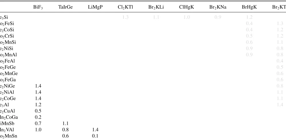
Second, there should be a good lattice match between the magnetic electrodes and the insulator. This is a necessary condition to ensure the epitaxial grow of the stack, which in turn is necessary for the spin filtering. We set the tolerance for the lattice match to less than 1.5%. Such match can be achieved either by having a one-to-one match between the insulator and the magnet (the two share the same crystallographic axes) or by rotating one of them by 45◦in the plane of the stack [here we consider only the (100) growth direction]. TableVIpresents all the possible electrode (barrier) combinations having a lattice mismatch smaller than 1.5%, with the 45◦-rotated epitaxial structures being in gray.
From the table it is easy to note that there are only eight magnets presenting a lattice mismatch smaller than 1.5% with our chosen insulator, BiF3. Two of these, Mn2CoGa and
Mn2VAl, are Mn2-based Heusler alloys, which we exclude
TABLE V. Magnetic Heusler materials with aTC greater than 700 K considered as potential electrode. We report the Strukturbericht (SB) symbols, the experimental lattice constant (aexp[ ˚A]), the Curie temperature (TC[K]), and the magnetic order, FM=ferromagnetic, HFM= half-metal. Here “ferri” means that the magnetic order is ferrimagnetic, although the electronic structure is that of a half-metal.
Material SB aexp TC Magnetic ground state Ref.
Fe3Al D03 5.793 713 FM [53]
Fe3Si D03 5.553 840 FM [53]
Fe2CoGe D03 5.780 925 FM [54]
Fe2CoSi D03 5.645 1,025 FM [55]
Fe2CuAl A2 5.830 875 FM [54]
Fe2NiGe A2 5.761 750 FM [54]
Fe2NiAl L21 5.778 965 FM [56]
Fe2NiSi D03 5.671 755 FM [56]
Co2MnAl B2 5.671 710 HMF [57]
Co2MnSi L21 5.655 985 HMF [58]
Co2MnGe L21 5.749 905 HMF [59]
Co2MnSn L21 6.000 829 HMF [60,61]
Co2FeSi L21 5.640 1100 HMF [62–64]
Co2FeAl B2 5.737 1000 HMF [64–66]
Co2FeGa L21 5.751 1100 HMF [60,64]
Co2FeGe L21 5.743 981 HMF [64,67]
Co2CrSi L21 5.647 747 HMF [68]
NiMnSb C1b 5.903 730 HMF [69]
Mn2VAl L21 5.920 760 HMF (ferri) [70]
Mn2CoGa L21 5.873 740 HMF (ferri) [71]
often the ground state of Mn2-type alloys presents a complex
magnetic structure with ferrimagnetic order between the crys-tallographic inequivalent Mn ions (e.g., see Mn3Ga)[72]. This
[image:4.590.301.549.162.245.2]is a situation which is not suitable for a spin valve. We also exclude the half-Heusler, NiMnSb, which has a half-metallic
TABLE VII. Magnetic Heuslers considered as potential elec-trodes. The Strukturbericht (SB) symbols, the experimental lat-tice constant (aexp [ ˚A]), the magnetic moment per formula unit (μS [μB/f.u.]), and the Curie temperature (TC [K]) are given. In the two final columns we show the band symmetry (σ
[001] for spin σ =↑,↓) across the Fermi level along the [001] direction, which have been calculated in this work. For Fe3Al no minority spin band crosses
the Fermi level along the [001] direction (note that globally Fe3Al is
not a half-metal, but it is along [001]).
Material SB aexp μS TC ↑[001] ↓[001]
Fe3Al [53] D03 5.793 5.10 713 1,5 –
Fe2CoGe [54] D03 5.780 5.40 925 1,5 5
Fe2CuAl [54] A2 5.830 3.30 875 1,5 5
Fe2NiGe [54] A2 5.761 4.29 750 1,5 5,2,2
Fe2NiAl [56] L21 5.778 4.46 965 1,5 2,2
electronic structure, but it is prone to disorder that strongly modifies its magnetic properties [73]. The electronic structure of the remaining five electrode compounds has been calculated, the symmetry of the states at the Fermi-level has been analyzed, and it is summarized in TableVII. Given the symmetry of the relevant complex band in BiF3, the electrodes must present
bands with 1 symmetry at the Fermi level for only one spin channel along the [001] direction. All five remaining candidates meet this criterion.
When looking at the electronic structure of the five remain-ing Fe-containremain-ing magnetic Heusler alloys, we notice that all of them present bands at the Fermi level with both1and5 symmetry in the majority (↑) channel, while the symmetry of the minority one (↓) differentiates them. In two cases, Fe2CoGe
and Fe2CuAl, the minority Fermi surface is dominated by the 5 symmetry, while for other two, Fe2NiAl and Fe2NiGe,
TABLE VI. Materials combinations presenting a lattice mismatch smaller than 1.5%. This can be obtained with the barrier and the magnet sharing the same crystallographic axes, or by rotating one of them by 45◦(in gray).
BiF3 TaIrGe LiMgP Cl2KTl Br2KLi ClHgK Br2KNa BrHgK Br2KTl
Fe3Si 1.3 1.1 1.0 0.9 1.2
Co2FeSi 0.4 1.3
Fe2CoSi 0.4 1.2
Co2CrSi 0.5 1.2
Co2MnSi 0.6 1.1
Fe2NiSi 0.9 0.8
Co2MnAl 0.9 0.8
Co2FeAl 0.4
Co2FeGe 0.5
Co2MnGe 0.6
Co2FeGa 0.6
Fe2NiGe 1.4 0.8
Fe2NiAl 1.4 1.1
Fe2CoGe 1.4 1.1
Fe3Al 1.2 1.4
Fe2CuAl 0.5
Mn2CoGa 0.2
NiMnSb 0.7 1.1
Mn2VAl 1.0 0.8 1.4
[image:4.590.45.544.494.740.2]TABLE VIII. Calculated formation energy [16,42].
Atoms Lowest Heusler Lowest formation
formation energy (eV/atom) energy (eV/atom)
Bi, F BiF3−2.22 –
Al, F AlF3−2.11 –
Fe, F FeF3−1.33 FeF2−4.25
F, Al, Fe F2AlFe−0.78 –
Fe, Al, F FeAlF2−0.62 –
Fe, Al Fe3Al−0.22 –
both2 and2 bands are present (in the case of Fe2NiGe
there is also a5 one). Fe3Al sets a case on its own, since
there is a spin gap in the minority band. Note that this is not a complete spin gap, namely, Fe3Al is not a half-metal, but it is
present along the (100) direction. For this reason, among the different possibilities, we have then chosen Fe3Al as electrode
material. Fe3Al has highTC(713 K) [53] and only a 1.2% lattice
mismatch to BiF3. It has a D03structure (F m¯3m), Fe(I) atoms
occupy the Wyckoff positions 4a(0,0,0) and 4b(12,12,12), while Fe(II) and Al atoms occupy the 4c(14,14,14) and 4d (34,34,34) ones, respectively.
In Figs. 1(a) and1(c) we present the band structure for majority and minority spins along [001] (the proposed stack orientation). As we have seen, BiF3 filters states with 1
symmetry, which are present in Fe3Al only for the majority
band. In fact, along the [001] direction (→X ink-space) at EFthere is a wide1band originating from the Al 3sand Fe 4s
states in the majority spin channel [Fig.1(a)], and a band gap in the minority one [Fig.1(c)]. The first1contributions for the minority spin appear at±1.5 eV fromEF, providing a 3 V
window in which the device is expected to show a large TMR. Note that, as already mentioned, the material is not half-metal as the gap in the minority channel is only along the specific
→X direction, as shown in Fig.1(b).
C. Secondary phases
We now turn our attention to discuss the possibility of creat-ing secondary phases or interfacial defects at the Fe3Al/BiF3
interface. Our criterion for phase separation is that the two materials in the stack, namely, Fe3Al and BiF3, should be
thermodynamically well separated from any other phase con-taining the same elements. If we assume that an epitaxial growth can be maintained, we have to verify their thermody-namic stability against other competing Heusler structures. In TableVIIIwe present the calculated formation energy of likely Heusler phases created with Fe, Al, Bi, and F. Here we have investigated all the possible site occupancies and distortions within the Heulser structure. We observe that the lowest energy of formation is for BiF3. Therefore, if the growth can be
maintained in the Heusler structure, we would expect a clean junction to form. Importantly, there is no F-rich structure that also contains Fe with an energy of formation within 1 eV/atom from that of BiF3, so Fe diffusion into the barrier is not likely
reducing the probability that paramagnetic defects will be present to scatter the spin. However, if the growth quality is low, growth of non-Heusler phases becomes possible and FeF2
is likely to form.
FIG. 2. Atomic structure of the all-Heusler Fe3Al/BiF3/Fe3Al
spin valve. The system is periodic in the plane orthogonal to [001], which defines the transport direction.
III. THE ALL-HEUSLER Fe3Al/BiF3/Fe3Al SPIN VALVE
A. Zero-bias properties
The all-Heusler Fe3Al/BiF3/Fe3Al spin valve is
con-structed by stacking Fe3Al(001) on BiF3(001), as shown
in Fig. 2. Its transport properties are now systematically investigated. For our transport calculations the in-plane lattice constant is fixed ata0=5.836 ˚A, equivalent to the theoretical
cubic lattice constant of bulk BiF3. Fixing the in-plane lattice
constant induces a small tetragonal distortion in the semi-infinite Fe3Al(001) leads withc/a0=1.124 (the cell is relaxed
to a forces tolerance of 10 meV/A). Such a distortion has˚ negligible effects on the electronic structure of the electrodes. The interface energy, corrected for basis set superposition error, is found to be 3.78 J/m2. To put this in context, the computed Fe/MgO interface energy is reported to be 2.52 J/m2 [74],
namely, the Fe3Al/BiF3 interface seems to be stronger than
the Fe/MgO one. The Fermi level of the junction is found to lie approximately in the middle of the BiF3band gap, with a
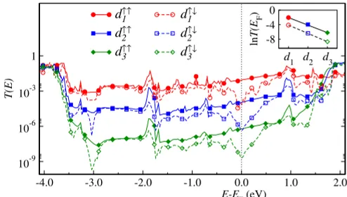
valence band offset of 3.06 eV, as shown in Fig.1(d). Electronic transport is calculated for three junctions with different BiF3thicknesses, respectively, of 13.10, 18.94, and
[image:5.590.304.551.517.657.2]24.77 ˚A. The zero-bias transmission coefficients as a function of energy,T(E), are shown in Fig.3and clearly demonstrate that there is an exponential reduction of the transmission with the barrier thickness, confirming that the transport mechanism is indeed tunneling with little contribution from possible interface states.
FIG. 4. k-resolved transmission coefficient at the Fermi level for the all-Heusler junction with a BiF3barrier of 18.94 ˚A. (a) Majority
spins parallel configuration, (b) minority spins parallel configuration, (c) antiparallel configuration. All results are obtained for a 100× 100k-mesh.
The various transmission coefficients for the [001] direction calculated at the Fermi level are plotted in Fig.4as a function of thek-vector in the two-dimensional Brillouin zone orthogonal to the transport direction. For the parallel configuration the transmission is dominated by the majority spins and ak-region around the-point, while for the minority band and for the an-tiparallel configuration the transmission is small and originates from narrow pockets ofk-vectors away from. This further confirms that the transport is dominated by the1symmetry, present only for the majority spins. Importantly, the relative contribution to the total current of the majority spin channel relatively to the minority one in the parallel configuration will exponentially grow as the barrier thickness increases, meaning that for barriers thick enough the Fe3Al/BiF3system behaves
as a half-metal, exactly as Fe/MgO.
B. Finite-bias properties
[image:6.590.39.284.63.146.2]For the 18.94 ˚A-thick junction we have calculated the current and the TMR as a function of bias (see Fig.5). Cal-culations are performed on a 24×24×1k-point mesh non-self-consistently (the potential drop is not non-self-consistently evaluated; see Ref. [75]) and have been verified against a
FIG. 5. Total current density,I, and TMR versus bias voltages,
V, for the parallel and antiparallel magnetic configuration of the junction. Results are presented for a non-self-consistent calculation (the potential drop is not calculated self-consistently) using a 24× 24 k-grid and confirmed by a self-consistent one obtained with a 100×100 mesh (closed symbols at voltagesV =0,0.1,0.5 V). The BiF3thickness is 18.94 ˚A.
FIG. 6. Self-consistently calculated finite-bias transmission coef-ficientT(E;V) as a function of energy for the (a–c) parallel and (d–f) antiparallel magnetic configuration of the electrodes. The vertical dotted-lines are located atE=EF±eV /2; namely, they enclose the bias window. Note that the transition remains spin degenerate only in the case of zero bias for the antiparallel configuration.
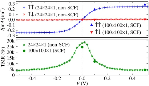
100×100×1 mesh for a self-consistent calculation at a few selected biases (0, 0.1, and 0.5 V). We find that the I-V characteristic of the parallel configuration is approximately linear at low bias and then saturates at about 0.2 V to a value of 0.25 mA/μm2. Since the same curve for the antiparallel
configuration is flat and the current is small, the TMR as a function of bias decays from theV ∼0 value of 25 000% to about 5000% at|V|>0.2 V [see below forT(E;V)]. This is indeed a very encouraging result since an extremely large TMR can be reached for a 2 nm think barrier, and larger values can be obtained by making the barrier thicker. We must note that the theoretical TMR is for the perfect junction and demonstrates that symmetry filtering is the dominant mechanism. The actual TMR of any junction will depend on secondary phases or defects at the interface, so the values observed here should be considered an upper limit.
The transmission of the Fe3Al/BiF3/Fe3Al junction has
been self-consistently calculated at 0, 0.1, and 0.5 V. In Fig.6 we present the transmission coefficient for each bias step, T(E;V). The behavior of the junction can be understood by considering the 1 filtering of BiF3 and the band structure
of the Fe3Al electrodes. We see that when the magnetizations
of the electrodes are parallel,T(E;V) for the majority spins is a smooth function of the energy, since the transmission originates from1band. At the same time there is no minority spin bands at the Fermi level along the [001] direction, resulting in a strongly suppressed minority transition aroundEF. As the bias voltage increases, bands with5,2, and2symmetry became available for transport. However, these are filtered by symmetry by the BiF3 barrier, and the transmission remains
[image:6.590.42.284.505.645.2]IV. CONCLUSION
In conclusion, we have identified from all known and predicted Heusler alloys a materials combination which can act as an alternative to the FeCoB/MgO/FeCoB heterostructure. In particular we have looked at the Fe3Al/BiFe3/Fe3Al stack
and demonstrated that this junction operates with the same symmetry spin-filtering mechanism of FeCoB/MgO and as such can display extremely high TMR values. Interestingly, the extended1spin gap along the (100) direction of Fe3Al
gives us a large energy window where to expect a significant TMR. As such for this proposed junction we expect a strong TMR retention at high voltage.
ACKNOWLEDGMENTS
This work was supported by the Higher Education Re-search Promotion and National ReRe-search University Project of Thailand, the Office of the Higher Education Commission, the Thailand Research Fund (MRG5980185), the Science Foundation of Ireland (14/IA/2624), and by financial support from the European Union’s Horizon 2020 PETMEM and TRANSPIRE projects. The authors wish to acknowledge the SFI/HEA Irish Centre for High-End Computing (ICHEC) and the Trinity Centre for High Performance Computing (TCHPC) for the provision of computational facilities and support.
[1] S. Ikeda, J. Hayakawa, Y. M. Lee, F. Matsukura, Y. Ohno, T. Hanyu, and H. Ohno,IEEE Trans. Electron. Devices54,991
(2007).
[2] S. Yuasa, T. Nagahama, A. Fukushima, Y. Suzuki, and K. Ando,
Nat. Mater.3,868(2004).
[3] S. S. P. Parkin, C. Kaiser, A. Panchula, P. Rice, B. Hughes, M. Samant, and S. Yang,Nat. Mater.3,862(2004).
[4] W. H. Butler, X.-G. Zhang, T. C. Schulthess, and J. M. MacLaren,
Phys. Rev. B63,054416(2001).
[5] J. Mathon and A. Umerski,Phys. Rev. B63,220403(2001). [6] A. Hoffmann and S. D. Bader, Phys. Rev. Appl. 4, 047001
(2015).
[7] T. Graf, C. Felser, and S. S. P. Parkin,Prog. Solid State Chem. 39,1(2011).
[8] T. Devolder, P.-H. Ducrot, J.-P. Adam, I. Barisic, N. Vernier, J. Kim, B. Ockert, and D. Ravelosona,Appl. Phys. Lett.102,
022407(2013).
[9] Y. Ando, K. Ichiba, S. Yamada, E. Shikoh, T. Shinjo, K. Hamaya, and M. Shiraishi,Phys. Rev. B88,140406(2013).
[10] C. Sterwerf, S. Paul, B. Khodadadi, M. Meinert, J. Schmalhorst, M. Buchmeier, C. K. A. Mewes, T. Mewes, and G. Reiss,
J. Appl. Phys.120,083904(2016).
[11] A. Kumar, F. Pan, S. Husain, S. Akansel, R. Brucas, L. Bergqvist, S. Chaudhary, and P. Svedlindh,Phys. Rev. B.96,224425(2017). [12] N. Tezuka, N. Ikeda, F. Mitsuhashi, and S. Sugimoto,Appl. Phys.
Lett.94,162504(2009).
[13] W. Wang, E. Liu, M. Kodzuka, H. Sukegawa, M. Wojcik, E. Jedryka, G. H. Wu, K. Inomata, S. Mitani, and K. Hono,Phys. Rev. B81,140402(R)(2010).
[14] S. Tsunegi, Y. Sakuraba, M. Oogane, K. Takanashi, and Y. Ando,
Appl. Phys. Lett.93,112506(2008).
[15] H. X. Liu, Y. Honda, T. Taira, K. I. Matsuda, M. Arita, T. Uemura, and M. Yamamoto,Appl. Phys. Lett.101,132418(2012). [16] R. H. Taylor, F. Rose, C. Toher, O. Levy, K. Yang, M. B. Nardelli,
and S. Curtarolo,Comp. Mater Sci.93,178(2014).
[17] E. Ozawa, S. Tsunegi, M. Oogane, H. Naganuma, and Y. Ando,
J. Phys.: Conf. Ser.266,012104(2011).
[18] H.-X. Liu, Y. Honda, K.-I. Matsuda, M. Arita, T. Uemura, and M. Yamamoto,Jpn. J. Appl. Phys.51,093004(2012). [19] T. Taira, T. Ishikawa, N. Itabashi, K. I. Matsuda, T. Uemura, and
M. Yamamoto,J. Phys. D42,084015(2009).
[20] T. Scheike, H. Sukegawa, T. Furubayashi, Z. Wen, K. Inomata, T. Ohkubo, K. Hono, and S. Mitani,Appl. Phys. Lett.105,242407
(2014).
[21] N. Tezuka, N. Ikeda, S. Sugimoto, and K. Inomata,Appl. Phys. Lett.89,252508(2006).
[22] Z. Wen, H. Sukegawa, S. Kasai, M. Hayashi, S. Mitani, and K. Inomata,Appl. Phys. Express5,063003(2012).
[23] N. Tezuka, N. Ikeda, S. Sugimoto, and K. Inomata,Jpn. J. Appl. Phys.46,L454(2007).
[24] N. Tezuka, S. Okamura, A. Miyazaki, M. Kikuchi, and K. Inomata,J. Appl. Phys.99,08T314(2006).
[25] T. Daibou, M. Shinano, M. Hattori, Y. Sakuraba, M. Oogane, Y. Ando, and T. Miyazaki,IEEE Trans. Magn.42,2655(2006). [26] J. Rogge, P. Hedwig, C. Sterwerf, and A. Hütten,IEEE Trans.
Magn.48,3825(2012).
[27] T. Marukame, T. Ishikawa, S. Hakamata, K. I. Matsuda, T. Uemura, and M. Yamamoto, Appl. Phys. Lett. 90, 012508
(2007).
[28] M. Yamamoto, T. Marukame, T. Ishikawa, K. Matsuda, T. Uemura, and M. Arita,J. Phys. D39,824(2006).
[29] T. Marukame, T. Ishikawa, S. Hakamata, K. I. Matsuda, T. Uemura, and M. Yamamoto,IEEE Trans Magn.43,2782(2007). [30] T. Kubota, S. Mizukami, Q. L. Ma, H. Naganuma, M. Oogane, Y. Ando, and T. Miyazaki,J. Appl. Phys.115,17C704(2014). [31] Y. P. Wang, G. C. Han, H. Lu, J. Qiu, Q.-J. Yap, R. Ji, and K. L.
Teo,J. Appl. Phys.114,013910(2013).
[32] C. Sterwerf, M. Meinert, J. M. Schmalhorst, and G. Reiss,IEEE Trans. Magn.49,4386(2013).
[33] Z. Q. Bai, Y. H. Lu, L. Shen, V. Ko, G. C. Han, and Y. P. Feng,
J. Appl. Phys.111,093911(2012).
[34] K. Nikolaev, P. Kolbo, T. Pokhil, X. Peng, Y. Chen, T. Ambrose, and O. Mryasov,Appl. Phys. Lett.94,222501(2009). [35] Z. Q. Bai, Y. Q. Cai, L. Shen, G. C. Han, and Y. P. Feng,Appl.
Phys. Lett.102,152403(2013).
[36] C. D. Pemmaraju, T. Archer, D. Sánchez-Portal, and S. Sanvito,
Phys. Rev. B75,045101(2007).
[37] A. Filippetti, C. D. Pemmaraju, S. Sanvito, P. Delugas, D. Puggioni, and V. Fiorentini,Phys. Rev. B84,195127(2011). [38] J. M. Soler, E. Artacho, J. D. Gale, A. Garcìa, J. Junquera, P.
Ordejón, and D. Sánchez-Portal,J. Phys.: Condens. Matter14,
2745(2002).
[39] N. Troullier and J. L. Martins,Phys. Rev. B43,1993(1991). [40] A. R. Rocha, V. M. Garcìa-Suárez, S. W. Bailey, C. J. Lambert,
J. Ferrer, and S. Sanvito,Phys. Rev. B73,085414(2006). [41] I. Rungger and S. Sanvito,Phys. Rev. B78,035407(2008). [42] http://www.materials-mine.com
[44] T. J. Moravec, R. A. Skogman, and E. Bernal G.,Appl. Opt.18,
105(1979).
[45] K. Kuriyama, K. Nagasawa, and K. Kushida,J. Cryst. Growth 237–239,2019(2002).
[46] K. Kuriyama, K. Kushida, and R. Taguchi,Solid State Commun. 108,429(1998).
[47] A. Roy, J. W. Bennett, K. M. Rabe, and D. Vanderbilt,Phys. Rev. Lett.109,037602(2012).
[48] F. Yan, X. W. Zhang, Y. G. Yu, L. P. Yu, A. P. Nagaraja, T. Mason, and A. Zunger,Nat. Commun.6,7308(2015).
[49] N. M. Caffrey, D. Fritsch, T. Archer, S. Sanvito, and C. Ederer,
Phys. Rev. B87,024419(2013).
[50] C. Ortiz, O. Eriksson, and M. Klintenberg,Comput. Mater. Sci. 44,1042(2009).
[51] Z. Yang, X. Wang, L. Liu, S. Yang, and X. Su,Comput. Mater. Sci.50,3131(2011).
[52] Z. Yang, X. Wang, Y. Pei, L. Liu, and X. Su,Comput. Mater. Sci.60,212(2012).
[53] T. J. Burch, K. Raj, P. Jena, V. Niculescu, J. I. Budnick, and W. B. Muir,Phys. Rev. B19,2933(1979).
[54] T. Gasi, V. Ksenofontov, J. Kiss, S. Chadov, A. K. Nayak, M. Nicklas, J. Winterlik, M. Schwall, P. Klaer, P. Adler, and C. Felser,Phys. Rev. B87,064411(2013).
[55] L. Hongzhi, Z. Zhiyong, M. Li, X. Shifeng, L. Heyan, Q. Jingping, L. Yangxian, and W. Guangheng,J. Phys. D40,7121
(2007).
[56] Y. J. Zhang, W. H. Wang, H. G. Zhang, E. K. Liu, R. S. Ma, and G. H. Wu,Physica B420,86(2013).
[57] T. Ryba, Z. Vargova, J. Kovac, P. Diko, V. Kavecansky, S. Piovarci, C. Garcia, and R. Varga, IEEE Trans. Magn. 51, 1
(2015).
[58] H. Pandey, P. C. Joshi, R. P. Pant, R. Prasad, S. Auluck, and R. C. Budhani,J. Appl. Phys.111,023912(2012).
[59] M. Belmeguenai, F. Zighem, Y. Roussigné, S. M. Chérif, P. Moch, K. Westerholt, G. Woltersdorf, and G. Bayreuther,Phys. Rev. B79,024419(2009).
[60] P. J. Brown, K. U. Neumann, P. J. Webster, and K. R. A. Ziebeck,
J. Phys.: Condens. Matter12,1827(2000).
[61] C. Felser and G. Fecher,Spintronics: From Materials to Devices
(Springer, London, 2013).
[62] S. Wurmehl, G. H. Fecher, H. C. Kandpal, V. Ksenofontov, C. Felser, H. J. Lin, and J. Morais,Phys. Rev. B72,184434(2005). [63] O. Gaier, J. Hamrle, S. Trudel, B. Hillebrands, H. Schneider,
and G. Jakob,J. Phys. D42,232001(2009).
[64] B. Balke, S. Wurmehl, G. H. Fecher, C. Felser, M. C. M. Alves, F. Bernardi, and J. Morais,Appl. Phys. Lett.90,172501
(2007).
[65] O. Gaier, J. Hamrle, S. Trudel, A. C. Parra, B. Hillebrands, C. H. E. Arbelo, and M. Jourdan,J. Phys. D42,084004(2009). [66] K. H. J. Buschow, P. G. van Engen, and R. Jongebreur,J. Magn.
Magn. Mater.38,1(1983).
[67] K. R. Kumar, K. K. Bharathi, J. A. Chelvane, S. Venkatesh, G. Markandeyulu, and N. Harishkumar,IEEE Trans. Magn.45,
3997(2009).
[68] X. Q. Chen, R. Podloucky, and P. Rogl, J. Appl. Phys.100,
113901(2006).
[69] C. N. Borca, T. Komesu, H. K. Jeong, P. A. Dowben, D. Ristoiu, Ch. Hordequin, J. P. Noziéres, J. Pierre, S. Stadler, and Y. U. Idzerda,Phys. Rev. B64,052409(2001).
[70] C. Jiang, M. Venkatesan, and J. M. D. Coey, Solid State Commun.118,513(2001).
[71] R. Y. Umetsu and T. Kanomata,J. Phys. Proc.75,890(2015). [72] K. Rode, N. Baadji, D. Betto, Y.-C. Lau, H. Kurt, M. Venkatesan,
P. Stamenov, S. Sanvito, J. M. D. Coey, E. Fonda, E. Otero, F. Choueikani, P. Ohresser, F. Porcher, and G. André,Phys. Rev. B87,184429(2013).
[73] D. Orgassa, H. Fujiwara, T. C. Schulthess, and W. H. Butler,
J. Appl. Phys.87,5870(2000).
[74] D. Wi´snios, A. Kiejna, and J. Korecki,Phys. Rev. B92,155425
(2015).
![TABLE IV. Insulating Heusler materials with a band gap E2we report the symmetry of the slowest decaying state along the [001]and experimental band gap (.5 eV](https://thumb-us.123doks.com/thumbv2/123dok_us/1541432.698531/3.590.308.551.61.311/table-insulating-heusler-materials-symmetry-slowest-decaying-experimental.webp)