TAKHAR, Jasbir S.
Available from Sheffield Hallam University Research Archive (SHURA) at:
http://shura.shu.ac.uk/20419/
This document is the author deposited version. You are advised to consult the
publisher's version if you wish to cite from it.
Published version
TAKHAR, Jasbir S. (2003). Test set generation and optimisation using evolutionary
algorithms and cubical calculus. Doctoral, Sheffield Hallam University (United
Kingdom)..
Copyright and re-use policy
All rights reserved
INFORMATION TO ALL USERS
The quality of this reproduction is dependent upon the quality of the copy submitted.
In the unlikely event that the author did not send a com plete manuscript
and there are missing pages, these will be noted. Also, if material had to be removed,
a note will indicate the deletion.
uest
ProQuest 10701065
Published by ProQuest LLC(2017). Copyright of the Dissertation is held by the Author.
All rights reserved.
This work is protected against unauthorized copying under Title 17, United States C ode
Microform Edition © ProQuest LLC.
ProQuest LLC.
789 East Eisenhower Parkway
P.O. Box 1346
Evolutionary Algorithms and Cubical Calculus
Jasbir S. Takhar
A thesis submitted in partial fulfillment of the requirements of
Sheffield Hallam University
for the degree of Doctor of Philosophy
I would like to thank, first and foremost, my supervisor Dr. Daphne Gilbert for her inspiration, encouragement and support throughout my PhD studies. There were many occasions on which her uplifting words would force me to think about a problem in another way or help me overcome the writer’s block that many a thesis-writer inevitably experiences. Without her hard work and dedication, this work would not have been possible.
I would like to acknowledge other members of my supervisory and advisory team for their support including Dr. Hugh Porteous and Paul Davies of Sheffield Hallam University and Dr. Anthony Hall of Hull University. I would also like to thank Dr. Mike Thomlinson, who as a senior member of The School of Science and Mathematics, provided help in both administrative and academic matters, including the funding that enabled my participation in the IEEE Midwest Symposium on Circuits and Systems in California, USA. I must also mention Prof. Bob Green and Dr. Hamid Dehghani both, of Sheffield Hallam University, for providing an excellent laboratory environment in which I conducted much of this work.
As the complexity of modern day integrated circuits rises, many of the challenges associated with digital testing rise exponentially. VLSI technology continues to advance at a rapid pace, in accordance with M oore’s Law, posing evermore complex, NP-complete problems for the test community. The testing of ICs currently accounts for approximately a third of the overall design costs and according to the Semiconductor Industry Association, the per-transistor test cost will soon exceed the per-transistor production cost. Given the need to test ICs of ever-increasing complexity and to contain the cost of test, the problems of test pattern generation, testability analysis and test set minimisation continue to provide formidable challenges for the research community. This thesis presents original work in these three areas.
Firstly, a new method is presented for generating test patterns for multiple output combinational circuits based on the Boolean difference method and cubical calculus. The Boolean difference method has been largely overlooked in automatic test pattern generation algorithms due to its cumbersome, algebraic nature. It is shown that cubical calculus provides an elegant and economical technique for solving Boolean difference equations. Formal mathematical techniques are presented involving the Boolean difference and cubical calculus providing, a test pattern generation method that dispenses with the need for costly circuit simulations. The methods provide the basis for test generation algorithms which are suitable for computer implementation.
Secondly, some of the core test pattern generation computations outlined above also provide the basis of a new method for computing testability measures such as controllability and observability. This method is effectively a very economical spin-off of the test pattern generation process using Boolean differences and cubical calculus.
The third and largest part of this thesis introduces a new test set minimization algorithm, GA-MITS, based on an evolutionary optimization algorithm. This novel approach applies a genetic algorithm to find minimal or near minimal test sets while maintaining a given fault coverage. The algorithm is designed as a post processor to minimise test sets that have been previously generated by an ATPG system and is thus considered a static approach to the test set minimisation problem. It is shown empirically that GA-MITS is remarkably successful in minimizing test sets generated for the ISCAS-85 benchmark circuits and hence potentially capable of reducing the production costs of realistic digital circuits.
CHAPTER 1. DIGITAL TESTING...4
1.1 In tr o d u c tio n... 4
1.2 Basic Term ino logy... 12
1.3 Fa ult Mo d e l s...13
1.3.1 Stuck-at F au lts...13
1.3.2 Bridging F aults...14
1.4 The Basicsof Test Pa ttern Gen era tio nfor Com binatio nal Logic Circuits...16
1.4.1 The Sensitive Path C on cept '...17
1.4.2 The Boolean D ifference M eth o d...20
1.5 Test Pa ttern Generation Algo rithm s...23
1.5.1 The D -Algorithm...24
1.5.2 PO D EM - Path O riented D Ecision M aking...28
1.5.3 FAN - Fanout-oriented Test Generation...31
1.5.4 A b rief com parison o f the D-Algorithm, PO D EM and FAN...33
1.6 Testability An a l y sis... 34
1.7 Re f e r e n c e s... 36
CHAPTER 2. TEST PATTERN GENERATION FOR MULTIPLE OUTPUT CIRCUITS USING CUBICAL CALCULUS AND THE BOOLEAN DIFFERENCE...40
2.1 In tro du c tio n... 40
2.2 Test Pattern Generationu sin g Boo lean Differences...40
2.2.1 Single Output C ase...40
2.2.2 M ultiple Output C ase...43
2.3 Propertiesof Boolean Functionswith Applicationstothe Boo lean Diffe r e n c e 43 2.4 The Calculusof Cu b e s...46
2.4.1 Cubical D efinitions and O perations...46
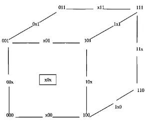
2.4.2 G eom etrical Visualisation...53
2.4.3 Exam ple to D educe a Minimum C over o f a Function...55
2.4.4 Approxim ate Optim isation Algorithm : SH RIN K...56
2.4 .5 The P * A lg orith m...58
2.4.6 Covers o f Com posite F unctions...61
2.5 Test Pa ttern Generation Using Bo o lean Differencesa n d Cu bic a l Ca l c u l u s... 62
2.5.1 D erivation o f Covers fo r Test Pattern G eneration...62
2.5.2 Test Set Generation Algorithm using Cubical Calculus - Single Output C ase 63 2.5.3 Test Set Generation using Cubical Calculus - M ultiple Output C ase...68
2.6 Testability An aly sisusing Cu bic a l Ca l c u l u s...76
2.8 Re f e r e n c e s... 81
CHAPTER 3. GENETIC ALGORITHMS...83
3.1 In tr o d u c tio n... 83
3.2 G A Ter m in o l o g y... 84
3.3 Sea rc h Spa c esa n d Fitness La n d s c a p e s...85
3.4 Genetic Algorithm Fu n d a m e n t a l s... 85
3.4.1 GA O verview...85
3.4.2 The Sim ple GA - An E xam ple...87
3.5 The Mathem atical Fo u n dationso f Genetic Alg o rith m s...92
3.6 G A Im plem entationis s u e s...100
3.6.1 Encoding Schem es...101
3.6.2 The Fitness Function...102
3.6.3 Selection... 104
3.6.4 C rossover...109
3.6.5 M utation...I l l 3.6.6 Selection o f GA O perator P robabilities...112
3.7 G A Applic a tio n s...113
3.8 Su m m a r y... 114
3.9 Re f e r e n c e s...115
CHAPTER 4. THE DERIVATION OF MINIMAL TEST SETS USING GENETIC ALGORITHMS... 120
4.1 In tro du c tio n... 120
4.2 Mo tiv a tio n...120
4.3 Applicationof G Asin Co m puter Aid ed Desig na n d Testof Integ r ated Circuits 121 4.4 A Su r v eyo f Test Set Minim isation Techniq uesa n d Algo rithm s... 123
4.5 Th e Minim al Test Set Problem... 127
4.6 GA-M ITS : Genetic A lgorithmb a se d M in im isa tio nof Te st Se t s... 129
4.6.1 ATPG D ata and the Generation o f a Fault M atrix...132
4.6.2 Encoding Scheme and Chromosom e Structure...133
4.6.3 The Fitness Function...134
4.6.4 Parent Selection Scheme used in G A-M ITS...135
4.6.5 Selection ofG A P aram eters...137
4.6.6 The Use o f Inoculation and Elitism...137
4.7 Circuitsu se dto Generate Fa ult Matricesfor G A -M IT S...137
4.8 Typical Perform anceof G A -M IT S... 139
4.10 Minim isation ResultsfortheISCAS-85 Ben ch m a rk Cir c u it s...144
4.11 GA-MITS Desig n Is su e s... 153
4.11.1 Inoculation o f the Initial P opulation...153
4.11.2 The Use o f an Exponential Ranking Scheme within G A-M ITS...157
4.11.3 Selection o f C rossover O perator and C rossover Rate...161
4.11.4 Selection o f M utation O perator and M utation R a te...166
4.11.5 Selection o f Population Size and N um ber o f Generations in a Run...167
4.12 Su m m a r y...169
4.13 Re f e r e n c e s...172
CHAPTER 5. CONCLUSION AND FURTHER W ORK...178
APPENDIX A. SOFTWARE LISTING: GA-MITS... 181
APPENDIX B. PUBLICATIONS...191
Chapter 1. Digital Testing
1.1 Introduction
Over the last three decades, the dramatic advances in VLSI technology have produced tremendous challenges for the test community. As circuits become larger and new fabrication techniques allow increased gate density, the complexity of digital testing increases exponentially. As this work will show, many of the problems in digital testing are NP-hard and as a result, their solution requires a multi-disciplinary approach. Many of these hard problems have been tackled with traditional, established techniques as well as some of the more recent innovations within the fields of computer science, engineering, and mathematics. Historically, digital testing has been a game of ‘catch-up’ with circuit design and manufacture technology. As soon as one test problem is adequately solved, the blistering pace of VLSI technology introduces new, even more complex problems. This can be seen today with the rapid approach of nanotechnology which seemingly renders traditional testing techniques, such as Iddq testing, as ineffective [1].
The microprocessor is the most important class of digital circuit and is, by far, the most complex. The microprocessor has changed the very fabric of everyday life in most parts of the world and continues to do so. As digital technology advances, giving rise to higher levels of integration, microprocessors increasingly find themselves in our everyday lives. In the late 1960s and early 1970s, integrated circuits and microprocessors superseded the slide-rule. In the 1980s they gave rise to the personal computer that today, provides more computing power on our desks than was used to put man on the moon. Over the last decade or so, advances in communications, including the internet and mobile technology, have changed the way people interact with one another. Looking ahead, the future for digital devices seems to hold promises of nanotechnology that may be as revolutionary as the microprocessor itself. One of the common threads in technology research has been to make things smaller and faster. Smaller and faster integrated circuits enable smaller and more powerful mobile devices for example. However, it is just this goal that gives rise to the enormous challenges in digital testing.
Gordon Moore, founder of the worlds largest microprocessor company Intel Corporation, made a very famous observation about the pace of change in the development and manufacture of integrated circuits. In his now famous paper [2], Moore predicted an exponential growth in transistor density on an integrated circuit and that this trend would continue for some decades. His observation, which was christened Moore’s Lawstates,
The number o f transistors on an integrated circuit doubles approximately every eighteen months, while the cost o f the circuit decreases by half
Moore made this prediction four years after the very first integrated circuit was developed in 1961 and over forty years later, his observation still holds true. Figure 1.1 illustrates Moore’s Law at work by graphically depicting the number of transistors in Intel’s family of microprocessors over the last thirty years or so.
Pentium s 4 Proc Pentium ft in P ro cess Pentium h H Frooe& sot /
transistors
f 100,000,000
MOORE'S LAW
10,000,000
8060
Boos
y
400 4 / y
Pentium R P ro c e sso r
10,000 100,000
1,000,000
1000
1970 1975 1980 1985 1990 1995 2000
Processor Name Year of introduction Transistors
4004 1971 2,250
8008 1972 2,500
8080 1974 5,000
8086 1978 29,000
286 1982 120,000
386™ processor 1985 275,000
486™ DX processor 1989 1,180,000
Pentium® processor 1993 3,100,000
Pentium II processor 1997 7,500,000
Pentium III processor 1999 24,000,000
Pentium 4 processor 2000 42,000,000
(b)
Figure 1.1 M oore’s Law illustrated by the history of Intel microprocessors. Figure (a) is a curve depicting the data points in (b) and shows the exponential growth in
the number of transistors on an integrated circuit. Reproduced courtesy o f Intel Corporation.
The world’s first microprocessor, the Intel 4004 introduced in November 1971, contained 2,250 transistors, ran at a clock speed of 108k Hertz and was able to perform 60,000 calculations per second. The 4004 is shown in diagram 1.2(a). As can be seen from the above curve, the number of transistors increase exponentially over the years and in 2000, Intel introduced the Pentium® 4 processor, which contained 42 million transistors and ran at an initial clock-speed of 1.5G Hertz. The Pentium 4 is shown in Figure 1.2(b). Intel states that, if over the same period, increases in car speeds kept pace with the increases in microprocessor speeds, one could cover the distance from San Francisco to New York (a distance of approximately 3000 miles) in 13 seconds. This fact alone illustrates the astounding developments in VLSI technology and gives some indications of the challenges faced by designers and testers alike.
(b)
Figure 1.2 (a) Intel 4004 microprocessor containing 2,250 transistors, introduced in 1971. (b) Intel Pentium® 4 microprocessor containing 42,000,000 transistors
introduced in 2000. Reproduced Courtesy o f Intel Corporation.
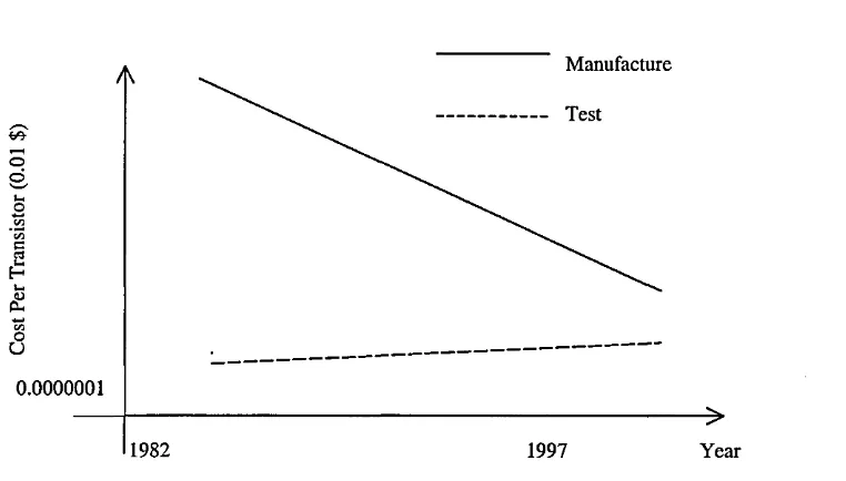
All of this VLSI research and development at the outer edges of our knowledge in such fields as chemistry, physics, engineering and mathematics is to be celebrated. However, these developments pose huge challenges for the test community who are in a continuous race to keep up. The costs associated with testing integrated circuits are huge and are of great concern to the semiconductor industry. In his paper [5] addressing many of the key issues in test, Kenneth Thompson of Intel, estimates his company spends a third of its capital expenditure on test and test equipment and he does not see this percentage decreasing any time soon. As further evidence of the increasing complexity and cost of test, the Semiconductor Industry Association (SIA), a well respected authority on the semiconductor industry, estimates that the cost of testing integrated circuits will actually surpass the cost of their production. The graph given in Figure 1.3 illustrates this.
Manufacture
Test
0.0000001
[image:16.613.135.516.267.484.2]1982 1997 Year
Figure 1.3 Fabrication and cost trends
T66SS
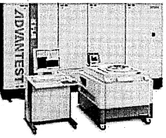
Figure 1.5 Automatic Test Equipment, model T6683, Advantest Corporation.
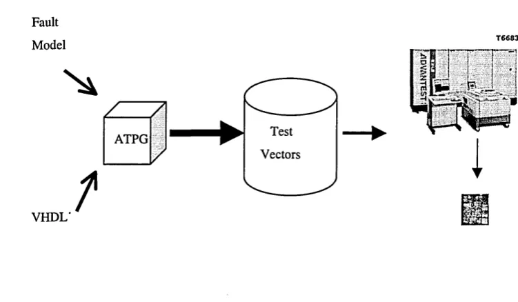
The purpose of test is, of course, to determine whether a circuit is defect-free and functions as intended. Under fault-free conditions, a given set of inputs to a circuit produces a corresponding set of outputs. In many cases, defects in the circuit will result in a deviation from the expected outputs. It is the detection of these deviations that is the central objective of post-fabrication digital testing. A circuit is tested by applying a given set of inputs, known as a test vector, and observing the output. For a given test vector, the fault-free output will be known and if the output deviates from this, a fault ewsawill have been detected in the circuit. The generation of these test vectors is known as test pattern generation. Test patterns are generated with a given fault (or faults) in mind and by generating a set of test vectors, known as a test set, a circuit can be tested for a given percentage of possible faults, known as the fault coverage. Once a test set has been generated, it is applied to an integrated circuit by automatic test equipment (ATE), which essentially observes the output in response to an input vector to determine whether the behaviour is as expected.
Fault Model
VHDL'
t
Test ATPG
[image:18.613.116.492.75.294.2]Vectors
Figure 1.4 High-level description of test pattern generation and test set application for integrated circuits.
As stated above, one of the roles of ATE is to apply test vectors to an integrated circuit and compare the output vectors with the expected outputs for a fault free-circuit. This test may only take a fraction of a second, but when faced with testing many millions of ICs a year, this is a huge cost burden for IC manufacturers. ATE equipment is itself getting quicker, but as ICs increase in complexity and gate density, so do the number of possible faults. This in turn often implies that a larger test set has to be applied by the test equipment to achieve the same level of fault coverage and for a given tester, this inevitably translates to greater test set application time. Again, the test community is faced with the challenges of Moore’s Law. Higher test set application times often translate into the need for more test equipment and therefore higher test costs. So, the need to reduce this test application time is critical for IC manufacturers in their continual quest for cost control.
Digital testing is a very large and diverse subject area, encompassing many disciplines. This thesis will describe the original work conducted by the author in three key areas of test; test pattern generation, test set minimisation and testability analysis.
Test Pattern Generation and Test Set Minimisation
take less time to apply to a circuit than ones that contain more test vectors. Given the complexity of integrated circuits, the process of actually generating the test patterns, is extremely challenging. The author will present a new technique for generating test patterns for combinational circuits that combines the Boolean difference [10] and cubical calculus [11]. The technique applies to multiple output, combinational circuits using the single-stuck-at fault model. Both the Boolean difference and the cubical calculus have been in existence for a number of decades but the Boolean difference technique has been overlooked within test pattern generation because of its cumbersome, algebraic nature. Cubical calculus is shown to overcome this problem and provides a very competent solution to this problem. Chapter Two will introduce cubical calculus and the Boolean difference and will provide a rigorous discussion on this new test pattern generation technique.
The increasing importance of minimised test sets in lowering test application time has already been discussed above. With this objective in mind, the author has successfully applied an evolutionary algorithm [12] to obtain minimised test sets. Chapter Three presents a detailed survey and analysis of a particular class of evolutionary algorithm known as a genetic algorithm . Once the reader has obtained an understanding of this optimisation method, Chapter Four goes on to describe the general problem domain of test set minimisation and the application of a genetic algorithm to solve the problem. The author developed genetic algorithm software to solve this problem for real-world test sets generating by a research group at Tallinn Technical University, Estonia. The data provided by this group and the software written by the author is described in Appendix A.
T estability A nalysis
Testability analysis provides a means of determining how difficult a circuit would be to test before it is actually manufactured. By performing this analysis during the design stage, circuit designers are able to catch features in a circuit that would make certain faults difficult (or impossible) to detect, resulting in design modifications at an early (and less expensive) stage in the life-cycle of a circuit. Following the work on test pattern generation using cubical calculus and the Boolean difference, a new technique for measuring testability was devised. It was soon realised that much of the core computations in the test pattern generation algorithm could be applied to calculate measures such as con trollability and
observability [7]. This work is presented in the final part of Chapter Two and will be shown to make novel use of the Boolean difference and cubical calculus.
generation algorithms that form the basis of many of the commercially available ATPG tools in use today.
1.2 Basic Terminology
As in most subject areas, there is much jargon and terminology in digital test. Consider the combinational, digital circuit in Figure 1.5. This circuit contains five logic gates; three AND gates, labelled G1 to G3, and two OR gates, labelled G4 to G5. The connections to and from the gates are known as circuit lines, lines or nodes. There are 5 primary inputs, PI1 - PI5 to the circuit and two primary outputs, POl and P02. The primary inputs/outputs to the circuit provide a means of connecting the circuit to the external environment. If the circuit were designed as an integrated circuit (IC), it would be contained in a plastic case and the primary inputs/outputs would be the pins of the IC, providing direct access to them.
PI1
G1
P O l G4
PI2
G2 PI3
PI4 G5 P02
G3 PI5
Figure 1.5 Combinational, digital circuit. The hashed line around the circuit illustrates the casing or packaging o f an IC.
Testing a digital circuit such as that given above involves applying sets of values to the primary inputs and comparing the corresponding outputs with the expected behaviour of the circuit. Each set of input values applied to the circuit is known as a test vector or test pattern and is often referred to as just a test. For a given test vector the corresponding, expected output is known as the fault-free output. In the above consider applying the values PI1=0, PI2=0, PI3=1, PI4=0, PI5=1. This set of input values produce fault free values at outputs POl and P 02 of 0 and 0 respectively. These inputs and the corresponding fault-free outputs constitute the test vector 00101100. The values 00101 to the left of the vertical line correspond to the inputs values at PI1, PI2 and so on and the values to the right correspond to the corresponding output values, POl and P02.
1.3 Fault Models
Circuit defects due to the manufacturing process for example, manifest themselves electrically as faults. In order to compile tests for faults one must establish a fault model that defines the relationship between a defect and a fault. A number of fault models exist and the popular ones will now be discussed.
1.3.1 Stuck-at Faults
One of the most popular fault models is the stuck-at fault model. In this model a line in a circuit is either permanently set or stuck-at-1 or stuck-at-0. Regardless of the logic value that should be present at the line under normal working conditions, a defect in the circuit has resulted in the line being stuck-at a given logic value. The abbreviations s-a-1 and s-a-0 denote stuck-at-1 and stuck-at-0 respectively. Consider the two input OR gate given in Figure 1.6. Input 1 is stuck-at-0 and when the test vector 1011 is applied to this gate, the actual output is 0 due the fault. In what conditions would a manufacturing defect result in a stuck-at fault?
s-a-0
Figure 1.6 Two input OR gate.
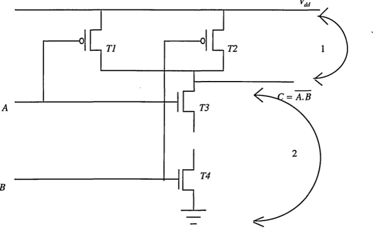
— T1
= A.B A
[image:22.613.163.533.47.277.2]B
Figure 1.7 CMOS implementation o f a two input NAND gate.
The numbers 1 and 2 signify two distinct defects in the circuit. Defect 1 is that the output of the gate has been short circuited with the power rail. This defect will result in the fault C s-a-1. Defect 2 on the other hand is a short circuit between C and the earth rail, resulting in the fault C s-a-0. These short circuit defects are common due to today’s manufacturing processes and can be conveniently modelled using the stuck-at fault model.
There are two different stuck-at models. A single stuck-at fault model in which it is assumed that only a single stuck-at fault is present in any given circuit and the multiple stuck-at model [8] which assumes multiple faults in a circuit. The model adopted in the present work is the single stuck-at model and this discussion will therefore be limited to this variant.
1.3.2 Bridging Faults
It must be noted that in general bridging faults are layout dependent and only occur between adjacent circuit lines. They differ from short circuits at the transistor level as described in section 1.3.1.
Figure 1.8 Combinational circuit with an input bridging fault between inputs 2 and 3, a feedback bridging fault between output 7 and input 1 and a non feedback bridging fault between lines 5 and 6.
Bridging faults cannot be tested using the stuck-at fault model since the bridged lines are able to assume both logic levels. If under fault free conditions two bridged lines assume the same logic value, then the circuit operation is unaffected. If however they assume complementary values a conflict arises. The actual logic values adopted in such a case depends on the technology used to fabricate the circuit as one logic value will dominate the other. In TTL logic (transistor-transistor logic) logic 0 dominates and if two bridged lines need to assume complementary values, both will be set to 0. In CMOS however, such a concept does not always apply and bridging faults have to be analysed at the transistor level [9, 10]. As this is beyond the scope of the present discussion, the reader is directed towards the references.
For s circuit lines, there is a total of s(s - 1) / 2 single bridging faults and obviously many more multiple bridging faults. Since the probability of bridging faults is higher for physically adjacent circuit lines, in general only faults between these lines will be tested for as it would be impractical to try and locate all bridging faults.
1.3.3 DELAY FAULTS
known as delay faults. There are two main types of delay faults, gate delay faults [15] and path delay faults [16]. The main difference between the two models is that the gate delay model can only cope with delays due to single, isolated defects whereas the path delay model can deal with the affects of distributed delays due to a number of defects. Delay faults cannot be tested using the stuck-at fault model as the fault behaviour does not affect the logical operation of a circuit. Other methods for testing delay faults exist and the reader is directed towards the references for further details [8], [17].
1.4 The Basics of Test Pattern Generation for Combinational Logic Circuits.
In general, electronic components and in particular integrated circuits, are very reliable devices. However due to imperfections in the manufacturing process that produce ICs, such as the presence of dust particles in the fabrication plant, faults will occur. Once the IC design has been finalised, the design engineer compiles a test set that may be applied to a device after it has been manufactured, to test for any defects.
For a non-redundant (meaning the function realised by the circuit under fault-free and fault conditions are different) combinational circuit containing n-inputs all faults may be tested by applying all 2" possible test patterns. This process of exhaustive testing, may be realised for small circuits but is impractical for circuits of say, 30 or more inputs. Exhaustive test pattern generation is obviously NP-hard since the number of test patterns increase as two to the power of n, the number of primary inputs. For example to exhaustively test a circuit containing 60 inputs there are 260 possible test vectors. If it were possible to apply 10,000 tests per second it would take approximately 3.5 million years to test a single circuit [8]. In practice however, it is unnecessary to apply all possible test vectors since a single test vector can cover a number of faults. The process of fault simulation [18] is used to determine which faults are covered by a given test vector. When the fault coverage of the test patterns has been generated it is possible to calculate the fault coverage of the test set. If there are x possible faults in a circuit and / faults can be detected by the test set, the fault coverage f c is given by,
f c =
-X
1.4.1 The Sensitive Path Concept
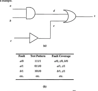
The first task of all test procedures is to compile a fault list, consisting of all the possible faults that can occur. As we are adopting the single stuck-at-fault model, it is assumed that these are the only faults that can occur. A test will then be written which will detect each fault in the fault list. Although each test may be written with the intention of covering one fault, it will invariably turn out in practice that it covers other faults in the list. To illustrate the basic principles of test, the circuit in Figure 1.9 (a) will be used as an example.
a
b
c
(a)
Fault Test Pattern Fault Coverage
a/0 111/1 a/0, zJO, b/0
a/1 011/0 a /1, zJl
b/l 101/0 b /l, zJl
etc. etc. etc.
[image:25.613.163.487.167.469.2](b)
Figure 1.9 (a) Circuit realising the Boolean function Z = a b
+
C (b) Partial fault list, test pattern and fault coverage table for (a)The Fault List
The first task when testing any circuit is to compile a fault list. The fault list for the above circuit is (the abbreviation x/0 means node x is stuck at logic value 0),
a/0 all b/0 b/l c/0 c/1 d/0 d/l e/0 c/1 zJO zJl
Testing isolated logic gates, where one has access to its primary inputs and outputs is a trivial task with the use of logic probes. However, it is often the case with combinational circuits that they contain internal nodes that one cannot directly access because they are housed in I.C. casings. In such situations the sensitive path concept is central to the testing procedure. The concept ensures that a fault at a node appears at the output of the circuit. If we assume there is an error at input a in Figure 1.9, a path has to be sensitised between it and the output, making the output dependent only on the value of input a. This is achieved by manipulating the values of b, c, d and e.
So, to sensitise the path between a and z, we must first transmit the value at input a to the output of the AND gate (node d) i.e. enable the gate. This is achieved by setting b to 1. Now, to transmit the value of node d through to z, we must enable the OR gate. This is done by setting node e to 0. To set e to 0 we have to work backwards and set node c to 1. So by setting, b=c= 1 we have sensitised a path between the input a and the output z.
Fault Cover and Test Pattern Generation
Once the fault list has been compiled, tests have to be written to cover each fault. There are two requirements when writing a test.
i) Establish the fault free condition. So if we are testing whether a node is stuck at 1, we have to set the node at logic value 0.
ii) Establish a sensitive path between the faulty node and the output.
Let us now write a test pattern for the first fault in the fault list, a/0. The sensitive path has already been calculated for input a, so to test for a/0 the test pattern is a=b=c= 1, giving a value of 1 at the output z. The test pattern is written as, 111/1. It was mentioned earlier that some test patterns will cover more than one fault and this is one of them. As we are seeking the logic value 1 at the output z, we are also in effect testing z/0. In a similar manner b/0 is covered. The procedure is now repeated for the remaining faults on the fault list. The table given in Figure 1.9(b) is a partial list of faults and their corresponding test vectors along with each test vector’s fault coverage.
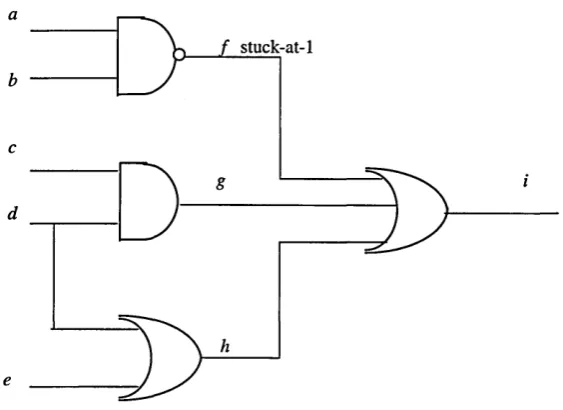
values at g and h. The required logic values are; c = 1 or 0, d - 0, e = 0, giving the test patterns 111001 1 and 1100011.
a
f stuck-at-1 b
c
d
[image:27.613.181.463.91.296.2]e
Figure 1.10. Combinational logic circuit with a stuck-at-1 fault at line f
Reconvergent Fan-Out and Undetectable Faults
Although most faults that may exist in a circuit can be detected, there are certain topological features that can make faults undetectable or difficult to test. As previously mentioned, testability analysis is a means to allow circuit designers to identify such features in their design before tape-out (i.e. a design is finalised).
1
Figure 1.11: z = a b .b c
Redundancy in a circuit can also create undetectable faults [8]. Often when one is seeking to sensitise a path, the situation arises where there are conflicting requirements e.g. a single gate needs to be set at the two logic values. In such cases testing difficulties have arisen because of the failure to minimise a circuit in the design stage.
Although they are not part of the simple stuck-at fault model, bridging faults, where two circuit nodes are accidentally connected together, are often included. Each node in a bridging fault can assume either logic value, the result depends on the type of technology used to implement the circuit. For example, in TTL (Transistor-Transistor Logic), the low node dominates and a high node will be pulled low. If the fault free value of each node is the same, then the circuit operation is unaffected. If however they are different, the fault needs to be detected and rectified. Similar techniques to those used for detecting stuck-at faults such as sensitised path are used to detect bridging faults. Unfortunately, as with reconvergent fan-out, some bridging faults are impossible to detect. Not all bridging faults can be included in the fault model. For a few thousand nodes there will be perhaps millions of node pairs. So in practice, only bridging faults involving adjacent nodes or tracks are included.
1.4.2 The Boolean Difference Method
The Boolean difference [8], [10], [11] method of test pattern generation relies on Boolean algebraic descriptions of circuit lines. The Boolean difference is essentially an XOR of two closely related Boolean functions. If g and h are functions then, in the notation of Boolean algebra,
where © denotes the XOR operation. Consider a Boolean function F(X) of a single output circuit,
It must be noted that the left hand side of the above equation is not a derivative, it is simply notation to represent the Boolean difference with respect to the primary input xt. The most important property of the Boolean difference which forms the basis of its use in test pattern generation is that
if and only if the output of the function F(X) is different for normal and erroneous settings of the primary input jq, in which case a fault at the primary input will be detectable, or observable, at the primary output. Conversely if
is true then F(X) is logically invariant under normal and erroneous settings of xt and a fault in xt cannot be detected at the primary output.
The solutions of equation (3) provide the input vectors that propagate a fault on line xt to the primary output. A test for jq exists if the other inputs can be chosen so that a change of logic value at xt produces a change of logic value at the primary output. To actually generate a test vector for xt stuck-at-0/ 1, this primary input must first be set to 1/0 and then the fault has to be propagated to the primary output. By performing a logical AND operation between the logic value at the at-fault-line opposite to the fault condition and equation (3) one is able to generate test patterns for stuck-at faults at x, . Thus the test vectors for jq stuck-at-0 and stuck-at-1 are given by the solutions of equations (4) and (5) respectively.
where X = ( x j , and the variables xlf...,x n represent the primary inputs. The Boolean difference of F(X) with respect to xt- is defined by
dF(x)
(2)
(4)
The above equations (4) and (5) generate test sets for faults at the primary inputs only. However, the ability to generate tests for faults at the internal lines of a circuit is of greater interest. For an internal circuit node, Sj say, the Boolean difference with respect to Sj becomes
where Sj is regarded as a pseudo primary input [6]. The solution of the Boolean equation
dF(x,Sj)/dsj =1 (6)
provides all the input vectors for which a stuck-at fault on Sj alters the primary output.
As in the previous discussion, to generate a test vector for Sj stuck-at-0/1, the node must first be set to 1/0 and the fault propagated to a primary output. An internal node, Sj, can be expressed as a function of the primary inputs, viz. Sj (X) = Sj , ..., xn) , and the solution of the Boolean equation
Sj(X) = k (7)
yields the input vectors that set Sj to k for k = 0,1. The input vectors required to propagate a fault at Sj to a primary output are given by the solutions to (6) above. To generate test patterns for a fault on S j, it is therefore necessary to solve both equations (6) and (7) simultaneously. Hence, for a circuit with n inputs and m outputs, the test sets T0 and 7] for Sj stuck-at-0 and stuck-at-1 respectively are given by the solutions of
. . « dFlX'S:)
To- # - I 1=1 dSj' " = 1 (8)
H x 'Si)
i=i
T{. SJ( X) . Z — — L = 1 (9)
where Ff (x) denotes the fth output, for i=l,....,m.
Aside property (1): d[F( X) + G ( X ) ] _
dXj
j F p o g g i e
e(X)mx)
9 T O , « ? ( * )dX; dX; dX; ClX:
property (2):
d[F(X)G(X)] = r { X ) d G ( X ) ^ c m dF(X) @ dF(X) dG(X)
dX: dX: dX: dX: dX;
property (3): dF(X)
dX: = 1 F(X) depends only on x.
Example 1.1
Under what conditions will an error in x j cause the output to be in error if / (x ) = XXX2
+
x 3 ? Since,F(x)= XxX2 + *3
—— = ^--- by property (1) above
dx\ dxx
= X3X2 by property (2)
dxj
= x3x2 by property (3)
dx:
where we have u sed = 0 if xt and x t are independent (or if i & j ) . The above result means that dxj
an error in x x will ensure the output is in error if and only if x3x2 = 1 , i.e. *3=0 and *2= 1. Hence if Xxis stuck-at-1, we need to set xx
=
0 and use x2= 1, *3 =
0 to detect the fault.1.5 Test Pattern Generation Algorithms
is left to the researchers to find efficient solutions by use of effective and robust algorithms coupled with efficient organisation of the underlying data through the use of novel data structures.
Given the size and density of integrated circuits, test pattern generation can be a very complex process and is a very active area of research. Many different approaches have been used to efficiently generate test patterns. These approaches include random test pattern generation [19], [20] in which the fault coverage for randomly generated test patterns, using fault simulation, is determined and used to form test sets. Pseudo-exhaustive [21] test pattern generation is a technique that tries to generate test patterns by trying to minimize the time required to exhaustively test a circuit by making use of circuit topology and input/output dependencies. Mathematical techniques such as graph methods [22] and statistical methods such as Monte Carlo [23] have also been used. In addition to algorithms based on some of the aforementioned and more traditional areas of mathematics, newer approaches have also been used in test pattern generation. These include evolutionary algorithms [24], [25] and cellular automata [26].
Many of the above mentioned approaches are underpinned by the basic processes of digital test pattern generation as described earlier in this chapter. Path sensitisation, simulation and the use of fault models are central to many ATPG algorithms regardless of their approach. These basic principles, as well as one or two others, were developed over the past two or three decades and form the basis of the early and now fundamental test pattern generation algorithms. Many of the techniques described in the previous paragraph therefore, also find themselves using these basic principles. The three algorithms described below, The D-Algorithm, PODEM and FAN, are widely recognized as the gold standard within the field of automatic test pattern generation and as such, must be described in any work on test pattern generation.
1.5.1 The D-Algorithm
The D-algorithm [7], [11], published by John Roth in 1960, is by far the most famous test pattern generation algorithm for combinational circuits and the single stuck-at fault model. Given its age, it still remains as the center piece of the field and other algorithms, including PODEM and FAN are essentially extensions of this seminal work. Roth used many important concepts in his work including the use of cubical complex notation, backtracking, error propagation and line justification. He also employed a five-valued composite logic system where,
X = x/x
1 = 1/1
0 = 0/0
D = 1/0
In the above notation, a/b implies that a is the value of a line under fault-free conditions and b is the value of the line under a fault condition. X represents ‘dont care’ or unspecified values. The most interesting notation is the D notation, which represents a fault on a line, and is central to the algorithm. To detect a stuck-at-0 error on a line one must first set the line to 1, represented by a D. Given the definition of D above, this implies the value at the line under fault-free conditions will be 1 and under the fault condition it will be 0. In a similar manner, a stuck-at-1 fault can be represented by a D .
In order to generate a test for a particular fault, the fault line is represented by either D or D (depending on the fault the test is being generated for) with all other lines initially set to X. The next step is to sensitise a path from this line to one or more primary outputs of the circuit by setting the unspecified values from X to either 1 or 0. This process is known as the D-drive. Then there is a backward implication process, starting from the fault line, back to the primary inputs of the circuit. In a similar manner to the D-drive stage, the circuit lines leading to the primary inputs are set to 1 or 0 in order to set the D value at the faulty line. If one is able to set the primary inputs of the circuits to either 1 or 0, without conflict, then a test for the fault has been generated.
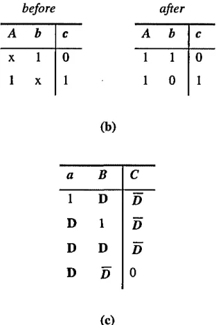
Before a detailed explanation of the algorithm is given, it is important to examine further, through example, the composite notation and the notion of singular covers. A singular cover is a compact representation of a truth table and each row in the cover is known as a singular cube. The singular cover for a two input NAND gate is given in Table 1. The truth table in (a) shows that when either (or both) of the inputs is set to 0, the output of a NAND gate is always 1, and when the inputs are both 1, the output is 0. An extended version of this table, using composite logic, is shown in Table 1(b). It illustrates some examples of backward implication. For example, in the before table, one row has c set to 0, b set to 1 and a unspecified. Through backward implication, it is obvious that for a NAND gate, a must also be set to 1. Another example in this table shows through backward implication, that b must be set to 0 if both a and c are set to 1. The final truth table in (c ) shows that D and D can imply both backward and forward implication.
A b c
0 X 1
X 0 1
1 1 0
before after
A b c A b c
X 1 0 1 1 0
1 X 1 1 0 1
(b)
a B C
1 D D
D 1 D
D D D
D D 0
(c)
Table 1.11 (a) Truth table for a NAND gate (b) truth table illustrating backward implication and (c ) forward and backward implication.
The D-algorithm also employs two key concepts; the J-frontier and the D-frontier, each being a list of gates that meet given criteria and are used to keep track of forward and backward implications. The J-frontier contains gates for which the output is assigned a logic value that is not implied by its inputs and for which no unique backward implication exists. For example, using the NAND gate as defined above, if a=b= x and c = 1 there are three ways to satisfy this output. That is, either a = 1, 6 = 0, or a = 0, b = 1, or a=b=0. Thus, no unique backward implication exists and these gates are candidates for line justification or backward implication. The D-frontier contains gates whose outputs are X and one or more of their inputs are D or D . These gates are candidates for D-drive as introduced above. A procedure o f imply-and-check is executed each time a line is set to a new value of 1 or 0 to ensure no conflicts have occurred. This procedure carries out all forward and backward implications based on the topology of the circuit. To explain the algorithm further, it will be used to generate a test for the stuck-at fault in the circuit given in Figure 1.12
To aid the discussion in the examples, the following notation will be used;
- P0 will denote the circuit line P stuck-at-0
[image:34.614.232.388.59.293.2]s-at-0
Figure 1.12 Combinational circuit with a stuck-at-0 fault at line F
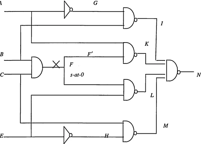
Example 1.2 Using the D-algorithm to generate a test for line F stuck-at-0 in Figure 1.12
The fault will be represented as F0 .
Step 1. Given the stuck-at-0 fault on F, we must set F - 1 and perform the imply-and-check based on this setting. The backward implication of this is that we must set B = C =1. This stage produces the D-frontier {K, L} and the J-frontier (j) , the empty set.
Step 2. Select a gate from the D-frontier through which to drive the value at F'. Select gate K.
To get D through gate K we need to assign A = 1(1) and we get K = D . Performing the ‘imply-and-check’ of these settings we see that,
G = 0 (1 ),7=1(1).
- this step produces the D-frontier { L, N} and the J-frontier (p.
[image:35.612.161.489.60.295.2]To drive the value through the primary output, we need to set L = 1(2) and M = 1(2). Carrying out the imply-and-check we see we require H = 0(2) and I = 1(2) which implies L = D (2) which is a conflict as L has already been set to 1 ! Given this conflict, the D-algorithm now has to perform its back tracking step. That is, to unset all the values set in the current step (i.e. step 2) and select a different gate from the D-frontier {L, N}.
Step 4. Select gate L.
To drive the value through L we need to assign E = 1. Performing the imply-and-check, we see that,
E = 1(2), 77= 0(2), M = 1(2) - this step produces the D-frontier {N} and J-frontier (j) .
Step 5. Drive D through N. This implies I = l(3).Performing the imply-and-check, we see that,
A = 1(3), G = 0(3),N = D
At this point we see that no conflicts exist, the D and J-frontiers are empty which in turn imply that all primary inputs have been set and that the fault has been driven through to the primary output. So a test vector for F stuck-at-0 is,
A - B - C - E - 1
As can be seen from the above example, the D-algorithm traverses the circuit, continuously driving faults through gates and performing the imply-and-check procedure to ensure no conflicts have occurred or been implied by the D-drive process. . If conflicts have occurred, an attempt is made to resolve them through back-tracking, which is just a systematic way of undoing the previous D-drive step and selecting another gate from the D-frontier and attempting the drive process through this new gate. For a given stage in the algorithm, if all gates in the D-frontier result in conflicts then no test exists for that fault. The above example is merely a description of how a test can be generated for one particular fault in one particular circuit. It gives some hints to the algorithm but a formal description of the algorithm is given is Figure 1.13.
1.5.2 PODEM - Path Oriented DEcision Making
faults in a circuit. The goal of PODEM was to reduce the heavy computational load of the D-Algorithm and achieved it by re-staging the problem in terms of a finite search space.
The D-Algorithm considers every node in a circuit to be part of the search space when trying to locate a test vector for a particular fault. Goel reduced the search space by confining it to include only the primary inputs since all other nodes may be expressed as functions of these.
Suppose we have a set of primary inputs that have been assigned either logic 1 or 0 and we set another primary input p, to logic value 1. As we propagate these primary inputs settings through to the primary output(s), much like the D-drive, and we encounter a conflict, we would only have to set the primary input p to 0 and see whether the conflict has been resolved. If this complimentary value also results in a conflict, this input is removed as a candidate for a test pattern, thus reducing the search space.
D-alg begin
if implyandcheck() = FAILURE then return FAILURE if(error not at Primary Output (PO) then
begin
if D-frontier = <J) then return FAILURE repeat
begin
select an untried gate (G) from the D-frontier
c = controlling value at G
assign c to every input of G with value x if D-alg() = SUCCESS then return SUCCESS end
until all gates from D-frontier have been tried return FAILURE
end
/* Error has been propagated to a primary output */ if J-frontier = § then return SUCCESS
select a gate (G) from the J-frontier
c = controlling value at G repeat
begin
select an input (j) of (G) with value x assign c to j
if D-alg() = SUCCESS then return SUCCESS assign cto j /‘ reverse decision*/
end
until all inputs of G are specified return FAILURE
end
Figure 1.13 High-level flow diagram o f The D-Algorithm
possible choices will have to be tried to resolve a conflict. PODEM attempts to resolve conflicts by resetting primary inputs only and then performing the D-drive process. It is this reduction in search space that gives PODEM the performance advantages over the D-Algorithm which will continually search all nodes in a circuit. In PODEM, as soon as a conflict is encountered, only a subset of the primary inputs need to be reset before the D-drive process is started once more.
When attempting to generate a test, PODEM begins by assigning all primary inputs the value X. It then aims to achieve what is known as an initial objective, which is to set the at-fault node to the opposite value to the fault-condition. The next stage of the algorithm is the backtrace, and this stage aims to obtain primary input assignments given the initial objective. It must then determine whether these primary input assignments have resulted in a conflict with the initial objective through the process of implication (PODEM uses circuit simulation to do this). If no conflicts have been generated, PODEM then selects another primary input and assigns a value to it and performs the simulation again to ensure no conflicts have occurred. If a conflict has occurred through this new setting, this primary input is then set to the complement of the initial setting to see whether this too causes a conflict (again through simulation). If a conflict occurs once more, then this primary input is removed from the search space and is no longer considered in the test generation process. If however, no conflict has occurred with either settings, the process of assigning another primary input repeats until a test has been generated or a conflict occurs or there is no path to propagate the fault to a primary output. The actual propagation to a primary output is performed in a similar manner as the D-Algorithm by searching for a path from the current D-frontier to one or more of the primary outputs. As an illustration of the algorithm, an example from [8] will now be discussed that uses PODEM to generate a test for a stuck-at-0 fault in the circuit in Figure 1.14.
Example 1.3. The use o f PODEM to generate a test for line 5 stuck-at-0 for the circuit in Figure 1.14
In the following discussion, the notion of a net will be used to describe the circuit topology. A net is essentially a circuit line that either feeds the input of a gate or leads from the output of a gate.
The initial objective is to set the output of gate A to 1. Then it is necessary to backtrace to one or more of the primary inputs. By backtracing, it can be seen that the input xx has to be set to 0 (x 2 could also have been selected). This input feeds net 1 so we set net 1 to logic 0.
1 2 3 4 5 6 7 8 9 10 11 12
O X X X X X X X X X X X
1 2 3 4 5 6 7 8 9 10 11 12
0 0 X X D X X X X X X X
Since net 5 is now specified, PODEM will now try to find a gate with D as its input and X as its output
towards the primary outputs, in a similar manner to the D-drive of the D-Algorithm. Gates G and H satisfy this condition. Selecting gate G and the subsequent initial condition results in the primary input
x3 being set to 0:
1 2 3 4 5 6 7 8 9 10 11 12
0 O O X D I X O X J J X X
x1 x2 x3 ;c4 = 000X is still not a test, so the PODEM must proceed. Given gate J has D on its input net 10, and Xs on input nets 9 and 11, the initial objective is now to set net 12 to logic 1 but we need to select net 9 as the next objective. This results in the primary input x4 being set to 0 as follows:
1 2 3 4 5 6 7 8 9 10 11 12 0 0 0 0 D 1 1 0 0 J) D D
Hence, now all primary inputs have been set and the fault can be propagated to a primary output, we have a test vector, jq x2 x3 x4 = 0000, for this particular stuck-at-0 fault.
The same test could of course have been found by the DAlgorithm but substantially more trialand -error would have been required due to the number of propagation paths and other consistency operations [8], [27]. Also, for untestable faults, there is much wasted effort when compared to PODEM. It is these features of PODEM and the search space reduction feature described above that gives it significant performance improvements over the D-Algorithm. In some cases, these improvements are an order of magnitude better in terms of both processor time and memory usage [27]. For a deeper explanation of the algorithm, the readers are directed to Goel’s paper and a number of undergraduate texts [7], [11].
1.5.3 FAN - Fanout-oriented Test Generation
The explanation of the FAN algorithm requires the introduction of new terminology. A bound line is the output of a gate that is part of a reconvergent fan-out loop. A line that is not bound is considered to be free. A headline is a free line that drives a gate that is part of a reconvergent fan-out loop. Let us consider the circuit in Figure 1.15 below. Lines H, I and J are bound lines; A, B, C, D, E, F are free lines and G, H and F are headlines. Because by definition, headlines are free lines, they are considered as primary inputs and can be set arbitrarily. So, during backtrace, if a headline is reached, it as though a primary input has been reached and the backtrace ceases.
Figure 1.14 Combinational circuit with stuck-at-0 at line 5
[image:40.612.114.491.175.487.2]Consider the circuit in Figure 1.16 [8]. Lets assume an initial objective to set line H to logic 1, thus testing for H stuck-at-0. PODEM would backtrace to C, D or E. Lets assume the backtrace is done via the path H-E-C which sets £ to 1. This would mean C = 0. But, this would result in F being set to 1, G to 0 and H to 0, which fails the initial objective. Now if the backtrace is performed along H-G-F-C instead, the initial objective is achieved. Thus, possibly two or more backtraces would be required by PODEM to achieve the initial objective.
Figure 1.16 Combinational circuit with stuck-at-0 fault on line H
FAN however, backtraces along multiple paths to the fan-out point, along say H-E-C and H-G-F-C ensuring the value 1 would be set at C, while all along, the initial objective is kept in mind.
Reconvergent fan-outs cause many conflicts when trying to backtrace to primary inputs. Only when FAN has traced all paths to a particular fan-out point, will the actual fan-out stem be assigned a value. PODEM on the other hand will backtrace from an initial objective all the way to a primary input, perform simulation and then detect a conflict if one is present. It is this additional effort that is avoided by FAN. By not proceeding with the backtrace until all paths have been traced to it, FAN is able to avoid conflicts before possibly reaching a primary input and without the need for costly simulation, as required by PODEM.
1.5.4 A brief comparison of the D-Algorithm, PODEM and FAN
as it performs test pattern generation. The problem with both of these algorithms is the early detection of conflicts and the wasted computational effort in determining this condition. Reconvergent fanouts are often the culprits of these conflicts and FAN tries to eliminate these early on the backtrace process by tracing along multiple paths towards the fanout stem. Only when all paths have been traced to these points and it has been determined that no conflict has arisen, will FAN continue simulating further along the circuit paths. This heuristic itself is largely responsible for the computational efficiencies FAN is able to achieve over PODEM and the D-Algorithm.
Performance comparisons have been made of the three algorithms [29] by collating the results from publications written by the researchers of each algorithm. Unfortunately performance comparisons are difficult as the algorithms have not been given the same problem set to solve. Not only this, but the implementation of these algorithms were in different languages for different hardware platforms (hardware in the 1960s cannot be compared to that of the 1980s!) so it is difficult to make direct and truly meaningful comparisons. But some results are available for PODEM and FAN and and do give some indication of the relative merits of each approach. Goel discussed comparisons between PODEM and a random pattern generator [27]. Testing 50,000 gates, in a time of approximately 1372 minutes on an IBM 370/168 machine, PODEM was able to achieve 89% fault coverage of approximately 90,000 faults, which was a marked improvement over the random approach. The largest example reported by the authors of FAN was a 20,000 gate circuit which it, in a time of 291 minutes on an NEC System-1000, was able to achieve 95% fault coverage of approximately 33,000 faults.
Although the above results compare ‘apples to oranges’ it seems apparent from the results presented in the respective papers that FAN certainly seems a marked improvement over PODEM in terms of computational performance. For further details of the results the reader is directed towards the references given above.
As was mentioned earlier, test pattern generation is a complex and continuous effort given the pace of development of ICs. The above three algorithms form the basis of many ATPG algorithms and continue to do so. This is evident is some of the more recent work that has emerged; SOCRATES [30] is based on the strategies within FAN, ATOM [31] improves on PODEM and STAR-ATPG [32] and SPIRIT [33] both incorporate and improve upon, a number of the heuristics used in both PODEM and FAN. It would seem that as ICs incrementally follow Moore’s Law, ATPG algorithms also improve incrementally to maintain this pace.
1.6 Testability Analysis
topology of the circuit i.e. its design. The testability of a circuit is normally regarded as a function of two measures, controllability and observability [36]. Some of the more popular definitions are defined at each node of a circuit as follows:
Controllability: This is the ability to control the fault-free logic value at a node from the primary inputs, so that any logic value can be placed on the node by manipulating the values of the primary inputs.
Observability: This is the ability to propagate the value of a node to one of the primary outputs, so that if there is a change of value
![Figure 1.15 Combinational circuit [8]](https://thumb-us.123doks.com/thumbv2/123dok_us/774228.583432/40.612.114.491.175.487/figure-combinational-circuit.webp)