Ion Channel Sensor on a Silicon Support
Michael Goryll1, Seth Wilk1, Gerard M. Laws1, Stephen M. Goodnick1, Trevor J. Thornton1, Marco Saraniti2, John M. Tang3 and Robert S. Eisenberg3
1
Arizona State University, Department of Electrical Engineering, Tempe, AZ 85287
2
Illinois Institute of Technology, Department of Electrical and Computer Engineering, Chicago, IL 60616
3
Rush Medical College, Department of Molecular Biophysics and Physiology, Chicago, IL 60612
ABSTRACT
We are buildinga biosensor based on ion channels inserted into lipid bilayers that are suspended across an aperture in silicon. The process flow only involves conventional optical lithography and deep Si reactive ion etching to create micromachined apertures in a silicon wafer. In order to provide surface properties for lipid bilayer attachment that are similar to those of the fluorocarbon films that are currently used, we coated the silicon surface with a
fluoropolymer using plasma-assisted chemical vapor deposition. When compared with the surface treatment methods using self-assembled monolayers of fluorocarbon chemicals, this novel approach towards modifying the wettability of a silicon dioxide surface provides an easy and fast method for subsequent lipid bilayer formation. Current-Voltage measurements on OmpF ion channels incorporated into these membranes show the voltage dependent gating action expected from a working porin ion channel.
INTRODUCTION
Biosensor design has become one of the major research topics during recent years. Combining biochemical detection mechanisms with conventional silicon-based electronic signal processing is particularly challenging. Gated ion channels inserted in lipid bilayer membranes are very promising candidates as biochemical transducers, because of their high sensitivity while still being selective. This setup has been used successfully for the detection of a variety of
biochemical reagents [1]. The lipid bilayer membranes, which form the host for the ion channel proteins, are typically formed across apertures in hydrophobic substrates, such as
polytetrafluoroethylene (PTFE, Teflon). Apertures in these substrates are prepared either mechanically or by electrical discharge [2,3], which both are low-volume production methods with limited reproducibility of hole size and shape. On the other hand silicon micromachining is already in a very mature state. Silicon, however, by itself does not have the properties required for a stable lipid bilayer formation. While silicon itself is hydrophobic, a natural oxide layer increases the surface energy, thus creates a hydrophilic surface on which lipid bilayer attachment is difficult. Surface modification layers that provide a low energy surface can facilitate the lipid bilayer formation and thus enable the combination between biochemical detection and
conventional silicon device architecture [4-7]. In this paper we will demonstrate that a plasma-deposited PTFE layer can provide the necessary surface modification to enable lipid bilayer attachment and subsequent ion channel insertion.
EXPERIMENTAL DETAILS
roughness on the lipid bilayer formation, double side polished substrates with 380 µm thickness were used as well. The aperture diameter for lipid bilayer attachment was designed to be 150 µm, similar to the geometry of existing PTFE systems [3]. To achieve an aspect ratio of about one between the thickness of the substrate and the aperture width, the area around the hole was thinned down to a thickness of 175 µm using reactive ion etching. Patterning of the structures to be etched was done using Novolak-based photoresist (AZ4330), which was exposed on a Canon UV mask aligner or a Heidelberg DWL66 direct laser writer.The laser writerwas used for backside alignment to center the aperture inside the prefabricated recess. The recess and the aperture etch were performed in a deep silicon reactive ion etching system (STS ASE tool) running the Bosch process with cyclic SF6 etch and C4F8 deposition steps. Samples were
thermally oxidized to form a 170 nm thick oxide layer that electrically isolates the surface from the bulk material. An additional 50 µm thick SU-8 epoxy resist layer was applies to one side of the sample and patterned using UV photolithography to decrease the capacitance of the samples in the measurement setup. As the last step, a PTFE layer was deposited in the STS deep silicon etching tool, using C4F8 as source gas. Thickness and refractive index of the layer were
characterized on a Woolam multiple wavelength ellipsometer and the water contact angle checked on a rame-hart measurement system. The subsequent lipid bilayer attachment experiments were performed using a mixture of the lipids (1,2-Dioleoyl-sn -Glycero-3-Phosphoethanolamine and 1,2-Dioleoyl-sn-Glycero-3-Phosphocholine) (DOPE:DOPC, 4:1) dissolved in Hexane. The sample was mounted between two PTFE chambers with 5 mm wide openings that provide access to the bilayer support area. Both chambers were filled with 3 ml of 1 molar potassium chloride (KCl) solution, buffered with 20 millimolar N-(2-Hydroxyethyl) piperazine-N'-(2-ethanesulfonic acid) (HEPES) at pH 7.4. Bilayers were formed by the painting method [2,8]. Bilayer resistance and capacitance measurements were carried out using an Axon Instruments Axopatch amplifier in connection with the pClamp software. Electrical access to the baths was achieved via two reversible Ag/AgCl electrodes immersed into the electrolyte
solutions. OmpF porin ion channels [8-10] were inserted into the membrane and their voltage-dependent gating mechanism was studied.
DISCUSSION
In order to measure a response from ion channels inserted in lipid bilayer membranes similar to previously reported Teflon solid support measurements, we tried to resemble the geometry of existing apertures as close as possible. The aspect ratio of the support is one of the important variables because of the torus formation in the lipid bilayer attachment region [11]. The size and shape of this torus influences the formation probability and stability of the lipid bilayer
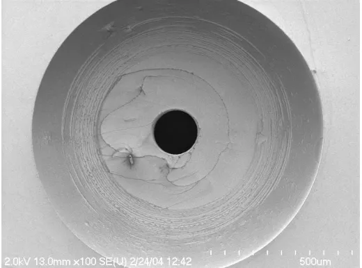
down the aperture size in future experiments without having to account for a varying etch rate, an aspect-ratio independent process was used as described in reference [13], with adaptations appropriate for our etching tool. The etch rate of this process is slightly lower at 3.7 µm/min, which still provides a fast process time. Fig.1 shows a SEM image of the aperture etched inside the recess area on a double side polished substrate.
The aperture itself exhibits excellent uniformity and smooth sidewalls. Using 100 mm (4”) wafers, good process controllability was achieved on a single wafer between multiple samples as well as between separate process runs. This allows for an improved reproducibility of the silicon-based microfabrication method described here over the conventional bilayer cup design.
Besides the geometrical requirements for the support, there is a demand for a specific surface energy of the substrate as well. Because the lipids are dissolved in an alkane, typically hexane or decane, the initial shape of the torus is determined by the contact angle between the solvent and the solid state support. Solvent contact angles on the currently used plastic bilayer cups and PTFE films are high, i.e. these materials have a low surface energy and thus are hydrophobic. Water contact angle measurements are used to determine the surface energy of a specific
material. Silicon dioxide surfaces on the contrary are hydrophilic, so they are not an ideal surface for the formation of a stable torus region. Moreover, due to the amphiphilic nature of the lipids, the attachment of the lipid monolayer itself is thought to be different on a hydrophilic support. Although it seems possible that lipid bilayers can be formed across an oxidized silicon aperture [14], the formation probability is low. This is why there is a need for a surface modification layer on the aperture to lower the surface energy. One way of achieving a hydrophobic surface is to form a self-assembled monolayer on the silicon dioxide surface by vapor deposition of
[image:3.612.75.335.432.625.2]fluoroalkanes [15]. A layer of long chain alkylsilanes docks onto the surface and increases the water contact angle up to 114º [15]. However, these monolayers can be affected in aqueous environment due to the low binding energy of the fluoroalkylsilanes to the silicon surface [16].
Because the sensor is supposed to be used in solution, long term stability of the surface
modification layer is an issue. An alternative method of lowering the surface energy is to deposit a material with a lower surface energy. Polytetrafluoroethylene (PTFE) films have been
successfully used as hydrophobic or release layers in MEMS applications [17,18]. These layers are deposited using plasma-enhanced chemical vapor deposition of fluorocarbon precursor gases [19]. The etching process used to fabricate the recess as well as the aperture involves a cycling between the deposition of a fluorocarbon film to protect the sidewalls and a subsequent etch. The deposition of the protective polymer layers in our case is very similar to the process described in [17-19]. However, these layers are amorphous and thin (typically less than 10 nm thick) because they are only intended to be a temporary protection. Our interest was to prove that these layers can be used to modify the surface for lipid bilayer attachment. Therefore the deposition time was increased to provide a thicker and more robust layer. The layer thickness on a silicon substrate was determined using multiple wavelength ellipsometry. The result of a measurement is depicted in Fig.2, along with a model curve derived by simulating the variation of the wavelength
[image:4.612.79.322.454.636.2]dependence using an isotropic Cauchy model [20]. No significant difference between model and experiment could be noticed when using an anisotropic model as described in [20], which indicates that although our layers are amorphous they are isotropic in nature. The value of the refractive index was found to be 1.36 for a layer of 91 nm thickness, being lower than that of bulk PTFE, which is reported to be 1.4 [18], but higher than that reported for spin-on amorphous films (DuPont Teflon AF) of 1.35. The difference between the refractive index for bulk material can be explained by the high level of crystallinity of bulk PTFE, while the layers deposited by plasma-CVD are amorphous in nature [21]. However, the refractive index as well as the isotropy of the layer indicates that the material deposited is dense and does not have air cavities. A water contact angle of 110º shows that the modified surface is very hydrophobic. Long term exposure to water over a week did not degrade the hydrophobicity or lift off the layer. These results show that the plasma deposited PTFE layers are suitable for lipid bilayer attachment experiments.
Their resistance to water and robustness [17], combined with the easy processing and conformal deposition characteristics [18] makes them an ideal surfactant.
Oxidized silicon samples coated with a 30 nm thick PTFE layer were mounted in a setup consisting of two chambers filled with 1 M KCl solution, buffered with HEPES at pH 7.4. Two 5 mm wide holes provided access to the silicon support chip. The lipid bilayers were formed across the aperture using the painting method, while the substrate was pretreated with the lipid mixture in decane as the solvent. The sealing resistance, which was derived from the slope of the I-V curve in Fig. 3, shows that a giga-Ohm seal could be established. Subsequently we were able to measure the voltage dependent gating behavior from an OmpF ion channel protein that
spontaneously inserted into the suspended lipid bilayer membrane after adding the protein to one bath solution. From Fig. 3 one can conclude that the behavior of the ion channel inserted into the membrane suspended across the PTFE-modified SiO2 surface is what can be expected from a
working porin ion channel. Thus we were able to prove that using a plasma-deposited PTFE layer, a microfabricated silicon substrate can be used as a valid lipid bilayer support, offering the option of a downscaling of the aperture with a significant advantage in signal-to-noise ratio in ion channel measurements [22,23] that recent results indicate [12].
CONCLUSIONS
[image:5.612.90.320.417.599.2]We demonstrate an all-silicon support structure for the attachment of freestanding lipid bilayer membranes for incorporating channel proteins. In the microfabrication of the structure only established tools such as optical lithography and deep Si reactive ion etching have been employed, making the process suitable for the integration with Si-based electronic components. The process described offers significant advantages over the classical mechanical aperture fabrication methods regarding reproducibility and scalability.
Figure 3. I-V characteristics of a lipid bilayer membrane, suspended across a 150 µm wide aperture in silicon that was coated with a 30 nm thick PTFE layer. While the black curve shows the response of the membrane without an ion channel inserted, the grey curve shows the
A PTFE surface modification layer was deposited using plasma CVD that reduces the surface energy and facilitates lipid bilayer formation. The physical properties of this layer are found to be very similar to bulk PTFE material. Measurements of the sealing resistance of a lipid bilayer attached to the 150 µm wide silicon aperture show that a giga-Ohm sealing resistance could be achieved. An OmpF channel protein could be inserted into this membrane and I-V measurements were obtained which demonstrate the voltage dependent gating expected from a porin ion
channel.
REFERENCES
1. M. Trojanovicz, Fresenius J. Anal. Chem. 371, 246 (2001).
2. M. Montal and P. Mueller, Proc. Natl. Acad. Sci. USA 69, 3561 (1972).
3. W. F. Wonderlin, A. Finkel, and R. J. French, Biophys. Journal 58, 289 (1990). 4. C. Schmidt, M. Mayer, and H. Vogel, Angew. Chem. Int. Ed. 39, 3137 (2000).
5. R. Pantoja, D. Sigg, R. Blunck, F. Bezanilla, and J. R. Heath, Biophys. Journal 81, 2389 (2001).
6. M. C. Peterman, J. M. Ziebarth, O. Braha, H. Bayley, H. A. Fishman, and D. M. Bloom,
Biomedical Microdevices 4, 231 (2002).
7. N. Fertig, M. Klau, M. George, R. H. Blick, and J. C. Behrend, Appl. Phys. Lett. 81, 4865 (2002).
8. T. A. van der Straaten, J. M. Tang, R. S. Eisenberg, U. Ravaioli, and N. R. Aluru,
J. Computational Electronics 1, 335 (2002).
9. S. W. Cowan, T. Schirmer, G. Rummel, M. Steiert, R. Ghosh, R. A. Pauptit, J. N. Jansonius, and J. P. Rosenbusch, Nature 358, 727 (1992).
10. K.-L. Lou, N. Saint, A. Prilipov, G. Rummel, S. A. Benson, J. P. Rosenbusch, and T. Schirmer, J. Biol. Chem. 271, 20669 (1996).
11. S. H. White, Biophys. Journal 12, 432 (1972).
12. M. Mayer, J. K. Kriebel, M. T. Tosteson, and G. M. Whitesides, Biophys. Journal 85, 2684 (2003).
13. A.A.Ayón, R. Braff, C. C. Lin, H. H. Sawin, and M. A. Schmidt, J. Electrochem. Soc. 146, 339 (1999).
14. M. Goryll, S. Wilk, G. M. Laws, T. Thornton, S. Goodnick, M. Saraniti, J. Tang, and R. S. Eisenberg, Superlattices and Microstructures (2004) (in press).
15. V. DePalma and N. Tillman, Langmuir 5, 868 (1989). 16. H. Tada and H. Nagayama, Langmuir 11, 136 (1995).
17. P. F. Man, B. P. Gogoi, and C. H. Mastrangelo, J. Microelectromech. Sys. 6, 25 (1997). 18. B. K. Smith, J. J. Sniegowski, G. LaVigne, and C. Brown, Sensors and Actuators A70, 159
(1998).
19. D. F. O'Kane and D. W. Rice, J. Macromol. Sci. Chem. A10, 567 (1976).
20. K. K. S. Lau, J. A. Caulfield, and K. K. Gleason, J. Vac. Sci. Technol. A 18, 2404 (2000). 21. B. D. Washo, J. Macromol. Sci. Chem. A10, 559 (1976).
22. R. A. Levis and J. L. Rae, Methods Enzymol. 207, 66 (1992).
23. R. A. Levis and J. L. Rae, “Technology of patch clamp recording electrodes“, Patch-clamp Applications and Protocols, ed. W. Walz, A. Boulton and G. Baker (Humana Press,