The Microstructure, Thermal Fatigue, and Failure Analysis
of Near-Ternary Eutectic Sn-Ag-Cu Solder Joints
Sung K. Kang
1, Paul Lauro
1, Da-Yuan. Shih
1, Donald W. Henderson
2, Jay Bartelo
2,
Timothy Gosselin
2, Steve R. Cain
2, Charles Goldsmith
3, Karl Puttlitz
3,
Tae K. Hwang
4and Won K. Choi
51IBM, T. J. Watson Research Center, Yorktown Heights, NY 10598, USA
2IBM Microelectronics, Endicott, NY 13760, USA 3IBM Corporation, Hopewell Junction, NY 12533, USA
4Korea Adv. Inst. Sci. & Tech., Daejeon, Korea 5Samsung Adv. Inst. Tech, Suwon, Korea
The electronic industry is making substantial progress toward a full transition to Pb-free soldering in the near future. At present, the leading candidate Pb-free solders are near-ternary eutectic Sn-Ag-Cu alloys. The electronic industry has begun to study both the processing behaviors and the thermo-mechanical fatigue properties of these alloys in detail in order to understand their applicability in context of current electronic card reliability requirements. In recent publications, the solidification behavior of the near-ternary eutectic Sn-Ag-Cu alloys has been reported in terms of the formation of large Ag3Sn plates and their effects on mechanical properties of Pb-free solder joints. Several methods have been
employed to minimize the growth of the large Ag3Sn plates in the Sn-Ag-Cu solder joints by controlling the cooling rate during solidification,
reducing Ag and/or Cu content, or adding minor alloying elements which reduce the amount of undercooling required for the nucleation of tin dendrites. In the present study, the results of accelerated thermal cycle fatigue tests are reported with the near-ternary eutectic Sn-Ag-Cu alloys of reduced Ag contents. Changes in microstructure and mechanical properties are also discussed by comparing the solder joints before and after thermal cycling.
(Received September 10, 2003; Accepted December 2, 2003)
Keywords: lead-free solders, tin-silver-copper alloys, Ag3Sn plates, thermal cycling test, ball grid arrays (BGA), fatigue life, failure analysis, microhardness
1. Introduction
1.1 Near ternary eutectic Sn-Ag-Cu alloys
Among several candidate Pb-free alloy systems, the near-ternary-eutectic Sn-Ag-Cu alloys with a melting temperature around 217C are becoming a leading candidate,1–3)
espe-cially for SMT card assembly including BGA solder joints. The near-eutectic, commercially available alloys include 4.0Ag-0.5Cu, 3.9Ag-0.6Cu, 3.8Ag-0.7Cu, and Sn-3.0Ag-0.5Cu (in mass%). In a study of solidification behavior of the near-eutectic Sn-Ag-Cu alloys,4)it was reported that
Ag3Sn plate nucleation and ensuing growth may occur with
minimal undercooling. In contrast, the -Sn phase required significantly greater undercooling in order to induce nucle-ation and bring about final solidificnucle-ation.4,5) As a conse-quence of this disparity in the required undercooling for nucleation, large, plate-like Ag3Sn structures can grow
rapidly within the liquid phase, during cooling, before the final solidification of solder joints, as reported previously.6–8)
In addition, when large Ag3Sn plates are present, adverse
effects on the plastic deformation properties of the solder,7)
and plastic strain localization at the boundary between the Ag3Sn plates and bounding-Sn phase were observed.6)In a
study involving the thermo-mechanical fatigue testing of CBGA (ceramic ball grid array) solder joints,8) strain
localization was noted to occur at the boundary between the Ag3Sn plates and the-Sn phase, as well as preferred
crack growth along the -Sn/Ag3Sn interface. This study
also described the effective control of large Ag3Sn plate
formation by increasing the cooling rate and/or reducing the Ag content in Sn-Ag-Cu alloys.
1.2 Control of large Ag3Sn plate growth
The growth of large Ag3Sn plates in Sn-Ag-Cu alloys has
been extensively studied in terms of cooling rate,8–10) alloy
content,8,9) and minor alloying elements.11,12) The cooling
rate during the reflow of Sn-Ag-Cu alloys was found to be a critical factor in controlling the formation of large Ag3Sn
plates in SAC joints.8–10) At a high-cooling rate, such as
1.5C/s or higher, the formation of large Ag
3Sn plates can be
kinetically suppressed during a reflow process. However, providing a high-cooling rate is not always practical, especially, in the case of large thermal mass chip carriers. High-cooling rate operations can also cause unwanted side effects, such as thermally induced card warpage during assembly.
To thermodynamically suppress the formation of large Ag3Sn plates in Sn-Ag-Cu alloys, the Ag content was
reduced with a fixed Cu content.9,10)It was found that large
Ag3Sn plate formation was substantially reduced in alloys
having a Ag content less than 3 mass%, even under extremely slow cooling conditions, such as 0.02C/s.9)In addition, the
Cu content in Sn-Ag-Cu alloys was found to have a less significant effect than Ag content on the formation of large Ag3Sn plates. But, lowering the Cu content was also found to
be beneficial in reducing the so-called pasty range (the temperature range between liquidus and solidus temperature) of the molten solder, resulting in fewer joint defects.9)
Another method reported to control the growth of large Ag3Sn plates is to reduce the amount of undercooling
required for the solidification of -Sn.11,12) This can be achieved by adding minor alloying elements, such as Zn, Al, Sb and others to pure Sn or near-eutectic Sn-Ag-Cu alloys.13)
1.3 Optimization of Sn-Ag-Cu Alloy composition
It has been demonstrated that reducing the Ag content to less than 3 mass%, is a very effective method for minimizing the size of Ag3Sn plates in Sn-Ag-Cu alloys. The Cu content
appears to be less sensitive than Ag in forming large Ag3Sn
plates.9)But a high Cu content can lead to the formation of
large Cu6Sn5 rods in quantity, especially when Cu
metal-lization is used in the solder joint. In addition, a high Cu content in Sn-Ag-Cu alloys may increase the pasty range, causing a higher defect rate. Thus, using hypoeutectic alloys in both Ag and Cu content can be beneficial in suppressing both large Ag3Sn and Cu6Sn5particles and limiting its pasty
range, thus reducing the reliability risk factors associated with Sn-Ag-Cu solder joints.
An additional reliability concern associated with Sn-rich solders is the allotropic transformation of white tin (-Sn, tetragonal phase) to gray tin (-Sn, cubic phase) at temper-atures below 13C to form tin pest.9,14) Although tin pest
formation has not been reported with near-ternary Sn-Ag-Cu alloys, it would be prudent to modify the alloy composition to retard or prevent the formation of tin pest.
Based on this information, a series of modified Sn-Ag-Cu alloys was proposed for card assembly applications.9,15)One
example of a modified alloy composition is Sn-2.3Ag-0.5Cu-0.2Bi (mass%). A small addition of Bi content in the alloy can reduce the possibility of tin transformation as claimed in the literature.16)
In the present paper, thermal fatigue behavior of CBGA solder joints was investigated to assess the thermo-mechan-ical fatigue performance of the modified Sn-Ag-Cu compo-sitions. The study addresses the effects of Ag-content, cooling rate, and thermal cycle conditions. Changes in the microstructure and mechanical properties of solder joints during accelerated thermal cycling (ATC) tests are discussed as well.
2. Experimental Procedure
2.1 Test Vehicle description
ATC testing was conducted utilizing 230 mm280 mm (9 in.11 in.), mid-glass transition temperature (Tg) cards with
6 ceramic BGA modules attached as described in the previous study.17)The 4s4p cross-section of the cards results in a 1.8 mm (72 mil) nominal thickness. The card BGA module sites have circular, 0.74 mm (29 mil) diameter, non-soldermask defined pads. The pads are copper with an OSP surface finish. Using TMA, the effective CTE (coefficient of thermal expansion) for the card was determined to be 19 ppm/C in the module (BGA) areas and 16 ppm/C
outside or away from those locations. These card CTEs were approximately constant throughout the ATC testing temper-ature range.
The 32 mm32 mm ceramic modules containing a25
25I/O grid on a 1.27 mm pitch were used as the ATC test vehicle. The chip carriers were 0.8 mm (32 mils) thick and whose CTE was approximately 6 ppm/C. No chips were
attached to the carrier. Rather, a stitched pattern, provided within the carrier itself, was utilized for electrical monitoring. That is, the ceramic substrate wiring (i.e., daisy chain) and matching stitch pattern on the card, formed several
concen-tric rings of BGA solder joints after attachment to the card. Each BGA solder joint that was monitored as a part of a ring was essentially the same distance from the neutral point or DNP, the point on the card where there is no differential motion with temperature changes.
2.2 BGA Solder ball composition and card assembly
The substrate pads on a ceramic module for ball attach-ment were circular in shape with a diameter of 0.86 mm (34 mils) and had Ni-Au metallization. Solder balls were attached to the BGA substrate by placing 0.89 mm (35 mils) diameter solder balls on the BGA I/O pads and reflowing them in a ‘‘balls-up’’ configuration at a peak temperature of about 240C, using a water soluble flux. The compositions of the four Sn-Ag-Cu alloys investigated are given in Table 1. The commercial alloy, Sn-3.8Ag-0.7Cu (SAC) served as a control alloy for comparison purposes.
The BGA modules were joined to the test card with Sn-4.0Ag-0.5Cu solder paste reflowed in a forced convection oven under a N2atmosphere. Stencil printing of solder paste,
component placement and other process steps followed standard SMT practices. The solder paste volume averaged about 5,500 cubic mils per pad and was reflowed using a ‘‘ramp/soak/spike’’ type profile. The soak or plateau was at approximately 175C, peak temperatures were between 235–
240C, and time above liquidus was 70–75 seconds. Two
cooling rates were used, about 0.5C/s (slow) and 1.7C/s
(fast). The BGA solder joint height, or stand-off, was measured to be about 0.60 mm (23.5 mils) after card assembly for all alloys. Moderate void formation was found in the final solder joints due to the use of solder paste during card assembly. Void formation in the Pb-free solder joints was found to be equivalent to or slightly greater than normally found in similar Sn-Pb SMT assembled joints. The actual composition of the solder joints is expected to be slightly higher in the Ag content (by 0.15 to 0.2 mass%) than the composition of BGA solder balls, since the solder balls were attached using the Sn-4.0Ag-0.5Cu solder paste.
2.3 Accelerated thermal cycle testing
[image:2.595.305.549.95.172.2]After assembly, cards were electrically connected to the test system, mounted in fixtures, and placed in an ATC chamber. Four cards for each of the four alloys were run simultaneously in the same chamber. This procedure was undertaken to minimize any potential thermal profile dif-ferences during the comparative testing conducted on the
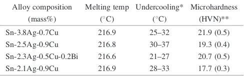
Table 1 Composition, Melting Temperature, Undercooling and Micro-hardness of As-received Sn-Ag-Cu BGA Solder Balls.
Alloy composition Melting temp Undercooling* Microhardness
(mass%) (C) (C) (HVN)**
Sn-3.8Ag-0.7Cu 216.9 25–32 21.9 (0.5)
Sn-2.5Ag-0.9Cu 216.8 30–37 19.3 (0.4)
Sn-2.3Ag-0.5Cu-0.2Bi 216.6 21–27 20.7 (0.5)
Sn-2.1Ag-0.9Cu 216.9 28–33 17.7 (0.3)
* Undercooling = onset melting temperature onset solidification temperature.
four alloys for each ATC condition. Thermocouples were attached to a minimum of four cards representing edge-to-center locations of the group within the chamber. The chambers were then run in load control and programmed until all thermocouples met the target thermal profile tolerances of
0=þ5C for the maximum profile temperature and
þ0=5C for the minimum profile temperature. The average
ramp rate was in the range of 12 to 14C per minute.
Three ATC test conditions were chosen with two temper-ature ranges (0 to 100C,40toþ125C) and two thermal
cycle frequencies (30 and 120 min) as follows; i) ATC Test#1: 0 to 100C, 30-min cycle time,
ii) ATC Test#2: 0 to 100C, 120-min cycle time,
iii) ATC Test#3:40to 125C, 42-min cycle time. For each ATC test cell, 24 modules were monitored using 4-wire interval readouts at room temperature. All BGA joints were tested at each readout. Failures were recorded when the change in resistance of an electrical net exceeded 200 m
from its initial resistance prior to thermal cycling. The data reported in this paper shows the cycle interval at which the first fail was identified for a particular module. In all cases, the location of the first fail was in the outermost, and highest DNP rings.
3. Results
3.1 The microstructure of solder joints after assembly
The microstructure of BGA solder joints after assembly has been examined on their cross sections for four alloy compositions and two cooling rates. Figure 1 shows a typical microstructure of a Sn-3.8Ag-0.7Cu joint located at a corner of a CBGA module. This solder joint was solidified at about
0.5C/s (slow cool) during the card attachment. The top (right) micrograph shows the microstructure near the ceramic module and the bottom (right) one is the microstructure at the card side. Due to the high Ag content and the slow cooling rate, large Ag3Sn plates grown in random directions were
commonly observed. In the case of the fast-cooling rate (1.75C/s) large Ag
3Sn plates were less frequently observed
in Sn-3.8Ag-0.7Cu joints. In solder joints with the reduced Ag content, large Ag3Sn plates were not observed in both the
slow and fast-cool conditions. However, the high-Cu content in the initial BGA solder and Cu dissolution from the Cu pad on the test card caused large Cu6Sn5rods to form near the
Cu-pad side. The presence of Ni is surprising in the CuSn IMC on the Cu pad in as-joined samples. This indicates that Ni diffusion occurred during joining through the molten solder from the Au/Ni pad on a ceramic carrier to the Cu pad on the card. A similar result was reported previously in the study of the interfacial reactions in Pb-free, BGA solder joints.18)The -Sn dendrite structure in fast-cool joints appears to be finer than in slow-cooled joints, while no apparent variation was noted among the ball locations; e.g.corner vs. middle of a ceramic carrier. However, the-Sn dendrites were observed to be finer near the interfaces, both on the ceramic carrier and card sides, than in the middle of the solder joints. In addition, the-Sn dendrite structure seems to be finer with a higher Ag content in Sn-Ag-Cu alloys.
It is interesting to note the presence of some curved Ag3Sn
[image:3.595.307.549.471.746.2]plates in the fast cooled, Sn-3.8Ag-0.7Cu joints, suggesting a complex growth behavior of large Ag3Sn plates.
Figure 2 exhibits another example of an as-assembled microstructure in Sn-2.5Ag-0.9Cu solder joints with a
η-Cu6Sn5
η-Cu6Sn5+ Ni
Ag3Sn Sn+Cu+Ni
60µm 60µm Sn-3.8Ag-0.7Cu
As-joined (slow cool)
Ag3Sn Sn-3.8Ag-0.7Cu
As-joined (slow cool)
Fig. 1 SEM micrographs showing a typical microstructure of Sn-3.8Ag-0.7Cu joint located at a corner of a CBGA module as-assembled with the cooling rate of 0.5C/s.
Sn-2.5Ag-0.9Cu
As-joined
(slow cool)
η-Cu6Sn5
η-Cu6Sn5+ Ni
60µm 60µm
Sn-2.5Ag-0.9Cu
As-joined
(slow cool)
[image:3.595.47.290.476.749.2]reduced Ag content. Here, large, primary Ag3Sn plates were
not observed anywhere even if the joints were cooled at a relative slow rate, about 0.5C/s. Due to the high Cu content
(0.9%),-Cu6Sn5particles were commonly noted in the
as-assembled microstructure. The -Sn dendrite structure was more or less similar in size regardless of solder ball location. But within a solder ball, a finer-Sn dendrite structure was observed near the interfaces compared with the middle of each solder joint.
3.2 ATC failure data analysis
[image:4.595.54.282.86.294.2]The electrical failure data from three different ATC test schemes were plotted as a lognormal probability distribution for 8 different test conditions (4 alloys and 2 cooling rates) in Fig. 3 to Fig. 5, respectively. Because of the field service conditions, the 0 to 100C ATC temperature range is
probably most widely used in the computer and communi-cation industries.
For the temperature range of 0 to 100C, two cycle times (30 and 120 min) were used. The number of cycles to failure in each case is plotted against the probability of accumulated failure rates in percentile for 8 different test cells in Fig. 3 and Fig. 4. Failure data was analyzed assuming lognormal statistics with a global common (all cells in every experiment were taken to have the same, which was found to be 0.1530). Parameters, obtained with the maximum likelihood method, are given in Table 2. [Note: The procedure for applying lognormal statistics is to take the natural log of the raw data, then use the more familiar normal statistics on the log of the data. Thus, ¼ln(N50), where
N50 is the cycle count corresponding to 50% accumulated
failure.] Because all of the experimental cells had the same number of parts with nearly complete failure, the significance of the factors and interactions were evaluated with a standard factor ANOVA (analysis of variance), again using the log of the number of cycles to failure.
As the cycle time is increased from 30 min to 120 min for the 0 to 100C temperature range, the number of cycles to
failure decreased in all cases, but more drastically for the SAC (Sn-3.8Ag-0.7Cu) and Sn-2.3Ag-0.5Cu-0.2Bi joints. This decrease in the number of cycle to failure is attributed to increased time for plastic strain accumulation and crack extension at the low and high temperature dwells and to the time-dependent changes that occur in the alloy microstruc-ture, particularly at elevated temperatures. For the 30-min cycle test, the average fatigue life (N50) is the largest for the
slow-cooled SAC joints, followed by the slow-cooled joints
Multiple Sample Lognormal Probability Plot Global Common σ = 0.153 99
95 90
75
50
25
10 5
1
Percentile
800 1000 1200 1400 1600 1800 Cycles to Fail
3.8Ag(slow) 3.8Ag(fast) 2.3Ag(slow) 2.3Ag(fast) 2.5Ag(slow) 2.5Ag(fast) 2.1Ag(slow) 2.1Ag(fast)
Failure Data for 0 C to 100 C (30 min Cycle Time)
Fig. 3 Comparison of the thermal fatigue life of Sn-Ag-Cu solder joints of CBGA carriers mounted on an organic PCB tested under the ATC condition of 0 to 100C with a 30-min cycle time.
Failure Data for -40 C to 125 C (42min Cycle Time)
Multiple Sample Lognormal Probability Plot Global Common σ = 0.153
200 300 400 500 600 700 800 Cycles to Fail
Percentile
99
95 90
75
50
25
10 5
1
3.8Ag(slow) 3.8Ag(fast)
2.3Ag(slow)
2.3Ag(fast) 2.5Ag(slow)
2.5Ag(fast) 2.1Ag(slow) 2.1Ag(fast)
Fig. 5 Comparison of the thermal fatigue life of Sn-Ag-Cu solder joints of CBGA carriers mounted on an organic PCB tested under the ATC condition of40to 125C with a 42-min cycle time.
Failure Data for 0 C to 100 C (120min Cycle Time)
99
95 90
75
50
25
10 5
1
Percentile
Multiple Sample Lognormal Probability Plot Global Common σ = 0.153
600 800 1000 1200 1400 Cycles to Fail
3.8Ag(slow) 3.8Ag(fast) 2.3Ag(slow)
2.3Ag(fast)
2.5Ag(slow)
2.5Ag(fast)
2.1Ag(slow)
2.1Ag(fast)
[image:4.595.314.531.102.272.2] [image:4.595.313.530.388.575.2]with 2.1%Ag and 2.5%Ag, and the fast-cooled joints of 2.1%Ag being the last. For the 120-min cycle test, this trend is reversed, where the slow cooled 2.1%Ag joints shows the longest fatigue life, followed by the slow-cooled 2.5%Ag, and the fast cooled 2.3%Ag (with 0.2%Bi) joints being the shortest. Here, the beneficial effect of low Ag content of Sn-Ag-Cu alloys on thermal fatigue life is clearly demonstrated for the 0 to 100C temperature range with the 120-min cycle
time.
Figure 5 shows the failure data for the 40 to 125C
temperature range with a 42-min cycle time. Because of the increased peak temperatures and the larger temperature range, the number of cycles to failure drastically decreased (to about 1/3) for the equivalent alloy and cooling condition compared to the 0 to 100C test. In addition, the spread in
fatigue life among the alloy compositions and cooling rates is much smaller compared to the 0 to 100C test. The 3.8%Ag
and 2.5%Ag solder joints performed slightly better than others.
In general, the slow-cooled joints survived longer than the fast-cooled joints for each alloy group for all three ATC test conditions.
3.3 Failure analysis of thermal cycled solder joints
Figure 6 shows a typical example of slow-cooled Sn-3.8Ag-0.7Cu BGA solder joints thermal cycled from 0 to 100C with the 120-min cycle. The four cross sections represent four different locations of solder joints; a corner solder joint (Ring-1), the second solder joint (Ring-2), the third (Ring-3) and the fourth (Ring-4) toward the center of the ceramic module. The temperature invariant solder joint at the center of a module, Ring-13, has a DNP value of zero. A dominant crack growth pattern is noted to be near the ceramic carrier side (top side of each micrograph), and no cracks are observed near the Cu pad on a PCB (bottom side). The crack propagation is observed up to the fourth ring of this module and the cracks are mostly confined to the pad/solder interface near the ceramic module. Large Ag3Sn plates that grew in
random directions are readily visible in the thermal-cycled SAC joints, but do not appear to have played a role in crack propagation.
Figure 7 shows another example of the cross sectional micrographs from BGA joints of Sn-2.5Ag-0.9Cu (slow cool), thermal cycled from 0 to 100C for 120 min. Because
of the reduced Ag content, no large Ag3Sn plates are noted in
these cross sections. In the Ring-1 joint, the cracks are observed both in the ceramic and in the Cu-pad sides. In this 2.5Ag joint, both cracks propagated much further into the solder joint compared to the 3.8Ag joints shown in Fig. 6. The failure analysis strongly supports the ATC test result that the low Ag joints (both 2.1Ag and 2.5Ag) have a longer fatigue life than the 3.8Ag joints tested for 0 to 100C with a
120-min cycle time.
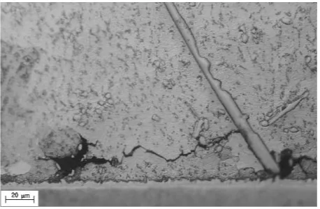
The interaction of Ag3Sn plates with the crack propagation
path is not clear from the cross sectional analysis of the present study, with regard to whether they facilitate or impede the crack propagation during thermal fatigue testing. Figure 8 depicts an example where the crack propagation appears to be blocked by the presence of a large Ag3Sn plate
in the crack path.
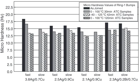
3.4 Microhardness measurement of BGA solder joints
[image:5.595.45.550.83.222.2]To investigate the changes in mechanical properties of BGA solder joints, microhardness measurements were performed on the cross-sections of thermal-cycled samples. Nine evenly spaced measurements were made on a33grid for each sample with a Vickers indentor using a load of 25 g. Figure 9 shows graphically the average microhardness of solder joints at a corner location of each module (Ring-1 position) in terms of solder composition, cooling rate and ATC scheme. The average microhardness of thermal cycled joints decreases as the ATC condition becomes more severe, such as with increasingTor cycle time in comparison with the as-assembled sample of each group. Except for the solder joints containing 0.2% Bi, the average hardness gradually decreases as Ag content decreases. It is not obvious to note the effect of cooling rate on the microhardness of solder joints either as-assembled or thermal-cycled. The microhard-ness measurement was also performed on solder joints at the center location of each module, where the DNP is zero. The average hardness reduction of the center location was less pronounced than at the Ring-1 position after thermal cycling. This can be understood by recognizing the fact that a solder joint at the center location only experienced thermal exposure, while solder joints at the corner experienced both thermal exposure and cyclic strain. The latter facilitate microstructural changes as well as crack growth in solder joints located at the corner.
Table 2 Average Fatigue Life (N50) Estimated from ATC Failure Data of Sn-Ag-Cu BGA Solder Joints.
Alloy composition ATC stress conditions
(cooling rate) 0 to 100
C 0 to 100C 40–125C
(30 min) (120 min) (42 min)
Sn-3.8Ag-0.7Cu (Slow) 1,408 (7.25)* 1,012 (6.92)* 455 (6.12)*
Sn-3.8Ag-0.7Cu (Fast) 1,164 (7.06) 982 (6.89) 392 (5.97)
Sn-2.5Ag-0.9Cu (Slow) 1,212 (7.10) 1,108 (7.01) 446 (6.10)
Sn-2.5Ag-0.9Cu (Fast) 1,200 (7.09) 1,054 (6.96) 384 (5.95)
Sn-2.3Ag-0.5Cu-0.2Bi (Slow) 1,212 (7.10) 953 (6.86) 407 (6.01)
Sn-2.3Ag-0.5Cu-0.2Bi (Fast) 1,130 (7.03) 934 (6.84) 376 (5.93)
Sn-2.1Ag-0.9Cu (Slow) 1,224 (7.11) 1,188 (7.08) 372 (5.92)
Sn-2.1Ag-0.9Cu (Fast) 1,064 (6.97) 1,012 (6.92) 384 (5.95)
Sample #11 3.8Ag, Slow Cooling
Ring-1 Ring-2
Ring-3 Ring-4
Fig. 6 Optical micrographs showing typical cross-sectional views of Sn-3.8Ag-0.7Cu solder joints thermal cycled from 0 to 100C with a
120 min cycle time. Four cross sections represent four different locations of solder joints, from a corner joint (Ring-1) to fourth joint (Ring-4) inboard.
Sample #59 2.5Ag, Slow Cooling
Ring-1 Ring-2
Ring-3 Ring-4
Fig. 7 Optical micrographs showing typical cross-sectional views of Sn-2.5Ag-0.9Cu solder joints thermal cycled from 0 to 100C with a
[image:6.595.98.498.68.364.2] [image:6.595.100.498.437.730.2]4. Discussion
4.1 Effects of Ag content
The microstructural characterization of both as-assembled and thermal-cycled joints identified large Ag3Sn plates in
Sn-3.8Ag-0.7Cu joints, but not in joints with a low Ag content, such as 2.5Ag, 2.3Ag or 2.1Ag. This is consistent with the previous results that the presence of large Ag3Sn plates was
critically influenced by the Ag content of the alloys.8–10)As
noted in Fig. 6, the characteristics of large Ag3Sn plates did
not change much in Sn-3.8Ag-0.7Cu solder joints after thermal cycling tests. This also agrees with the explanation previously given that the formation of large Ag3Sn plates
occurred during the solidification of solder joints.8–10) One of the objectives of the present study was to determine if there is any beneficial effects of a low-Ag content on the thermal fatigue life of Sn-Ag-Cu solder joints. Based on the ATC data analysis, there is an advantage of a low-Ag content on thermal fatigue life in the case of a 0 to 100C, long-cycle
time (120 min) stress condition, but not for a short-cycle time (30 min), nor for the40to 125C condition. For the 0 to
100C, 30-min cycle time test, Sn-3.8Ag-0.7Cu joints
exhibited a longer fatigue life than low-Ag joints, although large Ag3Sn plates were observed in the 3.8Ag joints. This
suggests the thermal fatigue behavior of Sn-Ag-Cu joints are more affected by thermal cycle conditions than the Ag content of the joints. Since large Ag3Sn plates are found in
random directions, the presence of large Ag3Sn plates may
not necessarily lead to a poor fatigue life. Considering an example shown in Fig. 8, where a large Ag3Sn plate appears
to block the crack propagation, the role of large Ag3Sn plates
on the fatigue life appears to be a complex issue.
One interesting result to note for low-Ag joints is that their fatigue life decreased to less extent as the cycle time increases compared to higher-Ag solder joints (e.g. Sn-3.8Ag-0.7Cu). The reduced sensitivity to cycle time for low-Ag joints can be explained based on microstructural dif-ferences observed among joints where Ag content differs. In particular, lowering Ag content in Sn-Ag-Cu alloys appears to reduce the volume fraction of the eutectic structure, and accordingly increase the volume fraction of -Sn dendrite phase. In addition, lowering the Ag content appears to
increase the Sn dendrite size. The microhardness measure-ments also support the changes in the microstructure; a decrease in microhardness as the Ag content decreases. The creep deformation of Sn-Ag-Cu alloys has been understood mainly by the deformation of the Sn dendrite phase rather than by the eutectic structure.19) Furthermore, since creep
deformation is known to be operative dominantly on grain or crystal boundaries, a coarse dendrite structure of low Ag joints is expected to be more resistant to the creep component of thermal cycling tests than high-Ag joints.
4.2 Effects of cooling rate
The beneficial effect of a slow-cooling rate is very clear in Table 2 for Sn-3.8Ag-0.7Cu joints, while the effect is less pronounced for low Ag containing joints, although the fatigue life of each alloy tested is slightly longer with slow cooling. When a solder joint is processed under a slow-cooling rate, it retains less residual stress and strain after solidification, so is a positive factor in enhancing fatigue life. Since Sn-3.8Ag-0.7Cu is the hardest and least ductile among the solders tested, it would benefit most from slow cooling. Interestingly, the beneficial effects of slow cooling seem to override potential deleterious effects of large Ag3Sn plates
found in slow-cooled joints of Sn-3.8Ag-0.7Cu.
Another factor to be considered in explaining the cooling-rate effect is the microstructural difference due to cooling rate. From this study and previous ones,9,10)slowly cooled joints (or alloys) exhibit a coarsened-Sn dendrite structure with a lower microhardness value in comparison to fast-cooled ones. When thermal fatigue would cause more time-dependent deformation such as creep than pure mechanical deformation, the coarsened microstructure observed in slow-cooled joints would exhibit a longer fatigue life.
The fact that the fatigue life of low Ag joints is more or less independent of cooling rate can be interpreted as an advantage of low Ag alloys, because they are less sensitive to reflow process conditions, including cooling rate, while Sn-3.8Ag-0.7Cu solder joints are significantly affected.
4.3 Thermal cycle effects
From the previous study of the thermal fatigue life of Pb-free solder joints in comparison to 63Sn-37Pb,17) it was reported that the thermomechanical fatigue behavior of Sn-3.8Ag-0.7Cu was much more sensitive to the choice of ATC temperature range and peak test temperature than eutectic Sn-Pb solder. It was also determined that the peak temperature, such as 125C, was a critical factor in reducing the fatigue
life of Sn-3.8Ag-0.7Cu for a given temperature range (T).17) In this study, it was determined (Table 2) that for
the same T¼100C, the longer cycle time of 120 min
reduced the fatigue life by 10 to 30%, and low-Ag joints were less affected compared to Sn-3.8Ag-0.7Cu. For the 40to 125C test (T¼165C) with a 42-min cycle time, the
fatigue life was drastically reduced to about 30% of the
T ¼100C condition. This reduction is attributed to the
higher peak temperature (125C vs. 100C) and larger T.
Even for the more extreme test condition of 40to 125C,
low-Ag joints survived better than Sn-3.8Ag-0.7Cu, although the differentiation is not remarkable.
The better thermomechanical behavior of low Ag joints
Fig. 8 Optical micrograph showing a large Ag3Sn plate blocking the
[image:7.595.55.284.599.749.2]over high Ag joints, especially under the ATC condition of 0 to 100C with 120-min cycle time, may be understood in
terms of their ductility or hardness properties. Based on the microhardness measurements of as-assembled joints (Fig. 9) and as-received BGA balls (Table 1), the hardness is generally lower when the Ag content is lower. This may imply that low-Ag joints have a higher ductility than high-Ag joints. The higher ductility would promote a better distribu-tion of accumulated plastic strain over a larger joint volume, and therefore exhibit a longer fatigue life. The crack extension per cycle is also reduced by the higher solder ductility. The crack propagation patterns observed with ATC-failed joints also support this argument as shown in Fig. 6 vs. Fig. 7. For Sn-3.8Ag-0.7Cu joints, the crack generally propagated along the interface between the module and solder, while for Sn-2.5Ag-0.9Cu joints cracks at each interface propagated further into the solder joint, suggesting more ductility and uniform distribution of plastic strain during the ATC test.
5. Conclusions
The thermo-mechanical fatigue behaviors of Sn-Ag-Cu solder joints have been investigated in terms of Ag content, cooling rate, and ATC test condition. From this study, the following conclusions are drawn:
(1) Sn-2.1Ag-0.9Cu solder joints assembled at a slow cooling rate have the best thermal fatigue life over the high-Ag joints for the ATC test of 0 to 100C with a 120-min cycle time.
(2) Sn-3.8Ag-0.7Cu solder joints assembled at a slow cooling rate have the best thermal fatigue life over other solder joints for the ATC test of 0 to 100C with a 30-min cycle time.
(3) The slow cooling rate (0.5C/s) is found to be beneficial
for the thermal fatigue life of Sn-Ag-Cu joints regardless of Ag content or ATC test scheme in comparison to the fast cooling rate (1.7C/s).
(4) The thermal fatigue life of low-Ag solder joints is less dependent of the cooling rate during the assembly process in
comparison to the high-Ag solder joints.
(5) The crack propagation pattern in Sn-3.8Ag-0.7Cu joints is more or less confined to the interface, while in low-Ag joints the crack propagation is within the solder joint. This suggests a longer fatigue life of low-Ag joints, possibly due to their greater ductility and lower hardness.
(6) The role of large Ag3Sn plates in determining the fatigue
life of Sn-Ag-Cu solder joints is not clear; being detrimental only when the plates are aligned in the direction of crack propagation. Notwithstanding the fact that the presence of a large Ag3Sn plate can actually enhance fatigue life by
blocking or arresting an advancing crack, it is also true they can significantly increase the reliability risk factor, thus every effort should be made to eliminate their presence.
REFERENCES
1) Japan Electronics and Information Technology Industries Association (JEITA), 2002 Lead-Free Roadmap.
2) J. Bath, C. Handwerker and E. Bradley: Circuits Assembly11(2000) 45–52.
3) I. E. Anderson, J. C. Foley, B. A. Cook, J. Harringa, R. K. Terpstra and O. Unal: J. Elec. Mater.30(2001) 1050–1059.
4) K. W. Moon, W. J. Boettinger, U. R. Kitten, F. S. Biancaniello and C. A. Handwerker: J. Electronic Mater.29(2000) 1122–1136. 5) I. Ohnuma, M. Miyashita, K. Anzai, X. J. Liu, H. Ohtani, R. Kainuma
and K. Ishida: J. Electronic Mater.29(2000) 1137–1144.
6) D. R. Frear, J. W. Jang, J. K. Lin and C. Zhang: JOM53(2001) 28–32. 7) K. S. Kim, S. H. Huh and K. Suganuma: Mater. Sci. Eng. A333(2002)
106–114.
8) D. W. Henderson, T. Gosselin, A. Sarkhel, S. K. Kang, W. K. Choi, D. Y. Shih, C. Goldsmith and K. Puttlitz: J. Mater. Res.17(2002) 2775–8.
9) S. K. Kang, W. K. Choi, D. Y. Shih, D. W. Henderson, T. Gosselin, A. Sarkhel, C. Goldsmith and K. Puttlitz: Proc. 53rd ECTC, (New Orleans, LA), May 2003, p. 64–70.
10) S. K. Kang, W. K. Choi, D. Y. Shih, D. W. Henderson, T. Gosselin, A. Sarkhel, C. Goldsmith and K. Puttlitz: JOM55(2003) pp. 61–65. 11) K. L. Buckmaster, J. J. Dziedzic, M. A. Masters, B. D. Poquette, G. W.
Tormoen, D. Swenson, D. W. Henderson, T. Gosselin, S. K. Kang, D. Y. Shih and K. J. Puttlitz: presented at the TMS 2003 Fall Meeting, Chicago, Nov. 2003.
12) S. K. Kang, D. Y. Shih, D. Leonard, D. W. Henderson, T. Gosselin, S. I. Cho and W. K. Choi: to be presented at TMS 2004 Annual Meeting, Charlotte, NC, March, 2004.
13) A. Ohno and T. Motegi: J. Japan Inst. Metals.37(1973) 777–780. 14) Y. Kariya, N. William, C. Gagg and W. Plumbridge: JOM53(2001)
39–41.
15) D. W. Henderson, T. Gosselin, S. K. Kang, W. K. Choi, D. Y. Shih, C. Goldsmith and K. Puttlitz: US Patent filed, Feb. 15, 2002.
16) W. G. Burgers and I. J. Groen: Faraday Society, Discussion23(1957) p. 183.
17) J. Bartelo, S. Cain, D. Caletka, K. Darbha, T. Gosselin, D. Henderson, D. King, K. Knadle, A. Sarkhel, G. Thiel, C. Woychik, D. Y. Shih, S. K. Kang, K. Puttlitz and J. Woods: Proc. APEX 2001, January 14–18, (San Diego, CA), (2001) LF2-2.
18) S. K. Kang, W. K. Choi, D. Y. Shih, P. Lauro, D. Henderson, T. Gosselin and D. Leonard: Proc. 52nd ECTC, (San Diego, CA), May 2002, pp. 147–153.
19) J. W. Morris, H. G. Song and Fay Hua: Proc. 53rd ECTC, (New Orleans, LA), May 2003, pp. 54–57.
0.0 2.5 5.0 7.5 10.0 12.5 15.0 17.5 20.0
22.5 Micro Hardness Values of Ring-1 Bumps As Joined 0 ~ 100 oC 30min ATC Samples -40 ~ 125 oC 42min ATC Samples 0 ~ 100 oC 120min ATC Samples
fast slow fast slow fast slow fast slow
3.8Ag/0.7Cu 2.5Ag/0.9Cu 2.1Ag/0.9Cu 2.3Ag/0.2Bi/0.7Cu
Micro Hardness (Hv)
[image:8.595.49.291.71.214.2]