Effects of Electrostatic Discharge Stress on Electrical Properties
of Bidirectional TVS Zener Diode with Abrupt Junctions
Daoheung Bouangeune
1, Yeon-Ho Kil
1, Sang-Sik Choi
2, Deok-Ho Cho
2,
Kyu-Hwan Shim
1,2,+and Chel-Jong Choi
1,3,+1School of Semiconductor and Chemical Engineering, Semiconductor Physics Research Center, Chonbuk National University,
Jeonju 561-756, Republic of Korea
2R&D Division, Sigetronics, Inc., Jeonju 561-756, Republic of Korea
3Department of BIN Fusion Technology, Chonbuk National University, Jeonju 561-756, Republic of Korea
A bidirectional transient voltage suppressor (TVS) Zener diode was fabricated with abrupt junctions using the low-temperature epitaxy process. The effects of various electrostatic discharge (ESD) stresses on the electrical properties are demonstrated, such as the currentvoltage (IV) and 1/f noise power spectral density (PSD). Very sharp and uniform bidirectional multi-junctions result in good symmetricIVbehavior over a wide range of operating temperatures of 300450 K. The differential resistance in the breakdown region is only 0.2³, and the reverse leakage current density is completely suppressed to 1.5©10¹4A/m2. The thermal activation energy obtained from the Arrhenius plot is nearly
equal to half the band gap of Si, indicating that the reverse leakage current is dominated by thermal generation at the depletion edges for the entire reverse bias regions. The manufacture bidirectional TVS devices exhibit excellent ESD robustness, regardless of the stress conditions of the human body model and electrical fast transient. However, a«4.5 kV machine model and«13 kV IEC61000-4-2 stresses led to severe damage of the epitaxially grown junction, resulting in rapid increases in both the reverse leakage current and 1/f noise PSD.
[doi:10.2320/matertrans.M2013144]
(Received April 12, 2013; Accepted August 21, 2013; Published October 11, 2013)
Keywords: electrostatic discharge (ESD), 1/f noise, transient voltage suppressor (TVS), zener, diode, human body model (HBM), machine model (MM), international electrotechnical commission (IEC), electrical fast transient (EFT)
1. Introduction
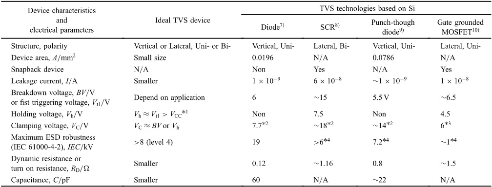
Electrostatic discharge (ESD) is a well-known transient threat to sensitive integrated circuit (IC) components.13) Common ESD events lead to permanent device damage associated with the breakdowns of junctions, metal inter-connects and dielectrics, caused by high current transients and high voltage overstress, resulting in the malfunction of IC chips. IC dimensions have been continuously scaled down to realize higher package density, faster operation speed and lower power dissipation. As such, ICs are more vulnerable than before to the damaging effects associated with ESD events.1,4)Moreover, ESD continues to be the primary cause of poor reliability in IC components. It was reported that approximately 35% of total IC failures are related to ESD, incurring tremendous annual costs to the IC industry.5,6) Therefore, dedicated ESD protection devices are required to protect IC chips against ESD damage. Among the various transient voltage suppressor (TVS) technologies as summa-rized in Table 1, the non-snapback TVS device like the TVS diode has received much attention close to an ideal TVS device, due to the simple structure and good performance characteristics, such as lowest leakage current, clamping voltage and dynamic resistance. Generally, the conventional TVS devices are constructed with reverse-biased pn junctions designed to breakdown at a well-controlled voltage, and operate in the avalanche condition.12)However, the large leakage current and capacitance make them unsatisfactory for high-performance technology applications.13,14)Furthermore, the conventional TVS devices are focused only unidirectional devices, despite the fact that ESD can have either a positive
or negative current/voltage waveform. Therefore, the bidirec-tional TVS device has emerged to ensure the reliability of the protective component.
We have fabricated a bidirectional TVS Zener diode with epitaxial Si layers consisting of very sharp planar junctions, and investigated the effects of ESD on its electrical properties. In particular, the currentvoltage (IV) and 1/f noise properties were analyzed in conjunction with ESD stresses to understand the failure process and correlate them to noise protection. It is shown that the manufactured TVS Zener diode is very promising, with a low differential resistance, good thermal stability and strong ESD protection capability.
2. Experimental Procedures
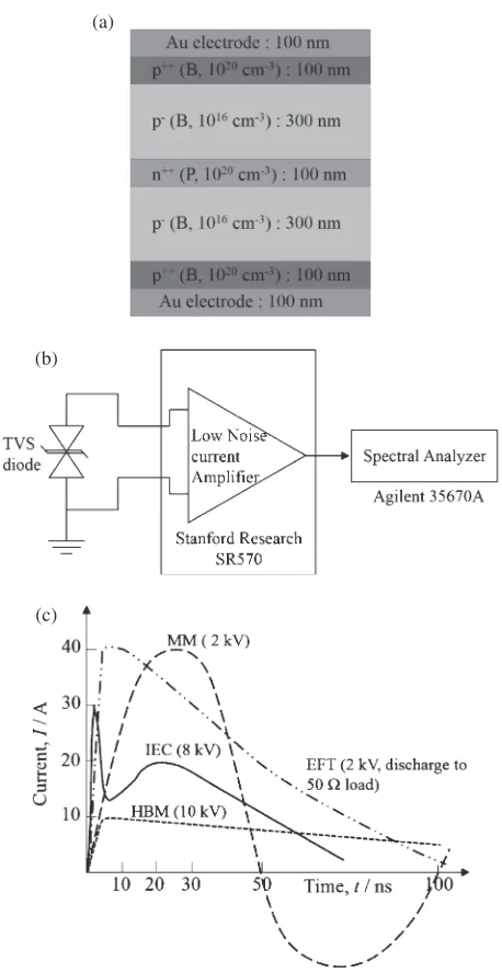
The proposed bidirectional TVS diode consisted of the pnp structure as the main part to avoid the snapback phenomenon compare the npn structure, as shown in Fig. 1(a).15)Although the snapback phenomenon can achieve low clamping voltage, the low holding voltage below power supply voltage is still main problem.8)In addition, a very thin and heavily doped n++epilayer enabledIVcurves steep rise after breakdown, resulting in small dynamic resistance value and the improvement of ESD performance. Therefore, the p-type (100) Si wafer with a resistivity of 0.003³·cm was used as a starting material. In addition, the bidirectional breakdown voltage was control by doping and thickness in multi-junction. To form an abrupt planar junction with a doping gradient of >5©1025cm¹4, thin Si films with various doping conditions were epitaxially grown using reduced-pressure chemical vapor deposition (RPCVD). The p- and n-type epitaxial Si layers in the junction were formed +Corresponding author, E-mail: khshim@jbnu.ac.kr, cjchoi@jbnu.ac.kr
in-situ by the addition of diborane (B2H6) and phosphine (PH3) gases during the deposition, respectively. To minimize the degradation of device performance caused by the non-uniform local electric field concentrated in the SiO2/Si interfaces associated with a linearly-graded junction formed by the conventional high-temperature drive-in process, the RPCVD process was performed at low temperatures of 600 800°C. For the same reason, based on the well-established complementary metaloxidesemiconductor (CMOS) tech-nology, the process temperature for the fabrication of a bidirectional TVS Zener diode was maintained below 800°C. In order to form a top contact electrode, 100-nm-thick Au film was deposited by means of an e-beam evaporator, followed by patterning with a 140©140-µm2 square shape using lift-off lithography. The details of the device structure and fabrication process for a bidirectional TVS Zener diode can be found elsewhere.16) The IV characteristics were analyzed using a parameter analyzer (Agilent 4156C). The ESD properties and reliably of the manufactured TVS diode were analyzed using an ESD simulator (NoiseKenESS-6008), which can supply an output voltage of up to «8 kV in a human body model (HBM) and machine model (MM). An ESS-2000 with a discharge gun TC-815R and FNS-AXII were used for the IEC61000-4-2 and IEC61000-4-4 standard analyses, respectively. For convenience, IEC61000-4-2 and IEC61000-4-4 are referred to here as IEC and electrical fast transient (EFT), respectively. The 1/f noise power spectral density (PSD) was measured using the experimental setup shown in Fig. 1(b), which consists of a low-noise current amplifier (SR570) and a spectral analyzer (Agilent 35670A). The HBM and MM tests referred as ESD simulator models represent the effect of statistic charges created by human body and machine discharge on electronic components. Generally, human bodies and machine components are charged by walking across a carpeted floor or removing a sweater, and by rubbing insulative materials during their operation, respectively.17) Meanwhile, IEC61000-4-2 and
IEC61000-4-4 are part of a larger family of IEC 61000-4 (IEC: International Electrotechnical Commission) defined as the performance required of all electronic devices in a variety of electromagnetic interference (EMI) conditions. The IEC was developed from HBM, which is referred as the minimum ESD level of acceptable performance required on all electronic devices sold into the European Union.18) The EFT test simulates the effect of the burst of very fast pulses on electronic components, which is created by switching circuits, such as relay contact bounce and some air contactors when interrupting inductive-capacitive loads.19) To under-stand the difference of each ESD models, all ESD waveforms used here were shown in Fig. 1(c).20,21)
3. Results and Discussion
Figure 2 represents the IV characteristics of a bidirec-tional TVS Zener diode measured at temperatures in the range of 300450 K. Generally, a bidirectional TVS Zener diode can be described as two unidirectional TVS diodes in back to back contact, i.e., one works in forward bias and another is reverse bias. When applied voltage or transient voltage like ESD is larger than breakdown voltage of TVS diode, the reverse biased one suddenly shows breakdown in avalanche breakdown mode, resulting in passing extra transient current to ground. For all temperatures, the device shows good symmetricIVbehavior without degradation of the device performance. The increase in temperature led to an insignificant change of the breakdown voltage, the value of which is ³«19 V at 102A/m2. Since the carriers in the semiconductor follow Boltzmann statistics, the reverse leakage current density increased with increasing temper-ature. However, regardless of temperature, the reverse leakage current density was kept at less than 10 A/m2 at
«15 V. This small reverse leakage current is essential to assure the improvement in reliability, noise performance and ESD robustness of the TVS device. The temperature
C/ Cµ h * ³ * ³ * *
Maximum ESD robustness
(IEC 61000-4-2),IEC/kV >8 (level 4) 19 >6*
4 7.2*4 ³1*4
Dynamic resistance or
turn on resistance,RD/³ Smaller 0.12 ³1.16 0.8 ³1.5
Capacitance,C/pF Smaller 60 N/A ³22 N/A
*1V
CC=Normal operator voltage of system or circuits.
*2Clamping voltage measured by transmission line pulse (TLP) at 10 A.
*3Clamping voltage at 1 A TLP.
[image:2.595.46.550.84.276.2]coefficients of the breakdown voltage and the reverse leakage current were measured to be ³10¹3V/K and
³3.42©10¹3A/m2·K (at ¹10 V). These values are reason-able, because Zener breakdown occurs correspondingly in the switching regime from the tunneling mode to the avalanche multiplication mode.22)
The temperature dependence of the reverse leakage current can provide useful insight into the leakage mechanism. The temperature dependence of reverse currentIrcan be described by:
Ir /T3exp EkTa
ð1Þ
wherekis the Boltzmann constant,Eais the activate energy of the junction andTis the absolute temperature. The slope of an Arrhenius plot of log10Ir(T)/T3 versus 103/T yields the activation energyEa.23)The activation energy of the reverse leakage current should in principle be close to the Si band
gap Eg or Eg/2 in diffusion or recombination-dominated regimes, respectively.24)Figure 3 shows the Arrhenius plot of the reverse leakage current of a bidirectional TVS Zener diode measured at various reverse biases in a temperature range of 300450 K. Irrespective of the reverse biases, the values of activation energy determined from the slope of the Arrhenius plots ranged from 0.56 to 0.57 eV, which are nearly equal to Eg/2. This result clearly indicates that the reverse leakage current of the bidirectional TVS Zener diode was dominated by thermal generation at the depletion edges for the entire reverse bias regions. The generation and recombination of carriers from generation-recombination centers in the space charge region of a pn junction in the present device could be a main contribution to carrier conduction in reverse bias.
The differential resistance (Rz=dV/dI) in the breakdown region is one of the most important parameters of the TVS device. A low differential resistance guarantees low clamping voltages and minimizes the resistive Joule heating with strong and rapid ESD surges. Moreover, the high differential resistance leads to unstable current drivability. Figure 4 presents the plots of differential resistance as a function of reverse current obtained from the IV characteristics in the Fig. 2 IV characteristics measured from the bidirectional TVS Zener
diode at various temperatures of 300, 350, 400 and 450 K.
Fig. 3 Arrhenius plot of the leakage current of a bidirectional TVS Zener diode measured at various reverse biases in temperature range of 300 450 K.
(a)
(b)
(c)
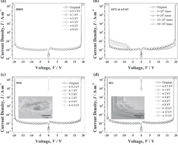
[image:3.595.55.284.66.510.2] [image:3.595.322.535.69.236.2] [image:3.595.322.526.292.452.2]application of various ESD stresses. The manufactured TVS at ¹10 V were respectively found to be 1.32©10¹4 and 2©10¹3A/m2 before and after applying 106 EFT pulses. Although the EFT stress led to the degradation of device performance to some extent, the reverse leakage current density level was still maintained below 10¹1A/m2. This implies that the TVS device demonstrated here has sufficient reverse leakage current margins for device application. Similarly, the TVS device was capable of withstanding
«4.0 kV MM and «12 kV of IEC without degradation of the IV characteristics, as shown in Figs. 5(c) and 5(d), respectively. However, both «4.5 kV MM and «13 kV IEC caused a rapid increase in the reverse leakage current density, indicating a typical electrical failure signature. The scanning electron microscope (SEM) results (insets of Figs. 5(c) and 5(d)) showed that the application of either«4.5 kV MM or
«13 kV IEC incurred the creation of pinholes surrounded by refrozen features on the metal electrode. This indicates that the epitaxially grown junction was severely damaged by
«4.5 kV MM or«13 kV IEC, which could be responsible for the device failure.
Fig. 5 IVcharacteristics measured before and after various ESD stresses: (a) HBM, (b) EFT, (c) MM and (d) IEC. Fig. 4 The corresponding differential resistance curves measured from the
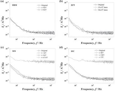
[image:4.595.61.276.251.415.2] [image:4.595.117.481.476.773.2]The ESD immunity of the bidirectional TVS Zener diode was also confirmed by low-frequency noise measurement, which is a valuable diagnostic tool to assess the reliability of semiconductor active devices.2528) Figure 6 exhibits the plots of 1/f noise PSD as a function of the frequency of the bidirectional TVS Zener diode measured before and after various ESD stresses. Similar to the ESD stress-dependent IV characteristics (Fig. 5), the manufactured TVS device showed excellent 1/f noise properties for HBM and EFT tests, as shown in Figs. 6(a) and 6(b), respectively. For instance, the 1/f noise PSD remained unchangeable (³10¹19A2/Hz at a frequency of 100 Hz) even after maximum HBM and EFT stresses. On the other hand, as shown in Figs. 6(c) and 6(d), the 1/f noise PSD changed insignificantly up to«4.0 kV MM and«12 kV IEC, and then increased rapidly. Such a large increase in the 1/f noise PSD could be associated with the defect-induced noise at the trap-and-detrap centers, when considering damaged features on of the present device produced by «4.5 kV MM and
«13 kV IEC (insets of Figs. 5(c) and 5(d)).
4. Conclusion
A bidirectional TVS Zener diode was fabricated with an epitaxially grown abrupt junction, and its ESD performance was demonstrated using IV characteristics and 1/f noise PSD. Due to the planar junctions achieved using low-temperature epitaxial growth technology, the reverse leakage current density and differential resistance in the breakdown region can be suppressed to 1.5©10¹4A/m2 and 0.2³, respectively. The manufactured TVS device presented an excellent ESD robustness against«8 kV HBM and 106EFT
pulses of 4.5 kV without degradation of theIVand 1/f noise characteristics. On the other hand,«4.5 kV MM and«13 kV IEC resulted in critical damage to the epitaxially grown junction, which could be responsible for the large increases in reverse leakage current and 1/f PSD.
Acknowledgements
This work was supported by the Priority Research Center Program (2011-0031400), and the Converging Research Center Program (2012K001428) through the National Research Foundation of Korea (NRF), funded by the Ministry of Education. It was also supported by the IT R&D program of the MKE (KI002083, Next-Generation Substrate Technology for High-Performance Semiconductor Devices).
REFERENCES
1) A. Z. Wang, H. G. Feng, K. Gong, R. Y. Zhan and J. Stine: Microelectron. J.32(2001) 733747.
2) M.-D. Ker and W.-J. Chang:IEEE Trans. Electron Devices55(2008) 14091416.
3) Z. Wang, H. Feng, R. Zhan, H. Xie, G. Chen, Q. Wu, X. Guan, Z. Wang and C. Zhang:IEEE Trans. Electron Devices52(2005) 1304 1311.
4) A. Amerasekera and C. Duvvury: IEEE Trans. Compon. Packag. Manuf. Tech. C18(1995) 314320.
5) R. Merri and E. Issaq: Proc. EOS/ESD Symp.15(1993) pp. 233237. 6) T. Green: Proc. EOS/ESD Symp. (1988) pp. 714.
7) D. Bouangeune, Woong-Ki Hong, S. S. Choi, Ch. J. Choi, D. H. Cho, J. M. Park, J. H. Lee, Hyun-Duk Yang and K. H. Shim: Proc. 1st IEEE GCCE, Tokyo, Japan, (2012) pp. 189192.
[image:5.595.115.483.71.364.2]IEEE Bipolar/BiCMOS Circuits and Technology, Boston, USA, (2007) pp. 226229.
16) S. S. Choi, D. H. Cho and K. H. Shim:Electron. Mater. Lett.5(2009) 5962.
17) J. E. Vinson and J. J. Liou:Proc. IEEE86(1998) 399420. 18) B. Jeppesen: Proc. Conference Northcon, Seattle, WA, (1998) pp. 134
Conf. on AIP.780(2005) pp. 721724.
27) L. K. J. Vandamme:IEEE Trans. Electron Devices41(1994) 2176 2187.