Interface Structure of Cu Wire Bonding on Cu Substrate with Sn Plating
Shinichi Fujiwara
1,+and Reinhold H. Dauskardt
21Yokohama Research Laboratory, Hitachi, Ltd., Yokohama 244-0817, Japan 2Stanford University, Stanford, CA 94305-4034, USA
In previous research on copper wire bonding on a copper substrate with tin plating, suitable thickness and binding conditions for the tin plating were chosen using the peel test after the copper wire bonding. These conditions were determined to be a thickness of 10 microns, a stage temperature of 373 K, a bonding power of 500 to 700 mW and a bonding time of 30 to 50 ms. Cross-sectional observations of the bonding interface indicated that the tin layer remained between the copper wire and copper substrate after bonding under these conditions. The purpose of the present study was to evaluate the joint interface structure of the bonded copper wire on the copper substrate with the tin plating. Residual Sn exists locally at the initial bonding interface, and the locations bonded to the interstitial Sn are intermixed with the locations where the Cu wire is bonded to a CuSn intermetallic compound. No oxidefilm layer was found at the bonding interface in the joint between the Cu wire and CuSn intermetallic compound; TEM images indicated that these have metallic bonding in which Cu and Cu3Sn are directly bonded. This is in contrast
to ultrasonic bonding between Cu and Sn, wherein the Cu and Sn are bonded by means of the Sn oxidefilm.
[doi:10.2320/matertrans.MB201203]
(Received June 1, 2012; Accepted August 16, 2012; Published November 25, 2012)
Keywords: wire bonding, interface structure, semiconductor device packaging, intermetallic compound, joint reliability, ultrasonic bonding
1. Introduction
Wire bonding has long been used for connecting the electrodes of semiconductor devices to external terminals, and currently remains the mainstream method for this purpose. Gold (Au) wires are most often used because they are easy to work with and exhibit superior corrosion resistance; they have been extensively investigated.1,2)
Meanwhile, pad pitches continue to decrease and by 2018, the minimum pad pitch is expected to be 30 µm and the minimum wire diameter 12.5 µm.3) However, because
bonding reliability decreases when Au reacts with the Al used for wiring in semiconductor devices,4)and neck breaks can
occur, increasing cost, as wire diameters become finer. Thus selecting a material to replace Au is a crucial problem. Ag, Al and Cu are being studied as a replacement for Au;58) of these, Cu is probably the strongest candidate for future
finer pitch applications due to its superior thermal and electrical conductivity, and its strength against neck breaks. However, Cu is difficult to form into uniform balls for ball bonding since it readily forms an oxide film in air. Cu also requires greater power during bonding since it is more difficult to deform compared to Au.
In the current research, we conducted a study of wedge bonding wherein wires are directly bonded without forming a Cu ball. In addition, Cu, which is widely used as the wiring material for substrates and leads, was selected as the material for the electrodes and external terminals to which the Cu wire was bonded, and the bondability of Cu wire to Cu substrates was evaluated. Cu wire bonding to Cu substrates has been previously studied; however surface oxidation of Cu remains a concern.911) In previous investigations,12)the Cu wires were bonded after suppressing the formation of oxide films on Cu by Sn-plating the Cu substrate, and parameters for bonding the Cu wire to the Cu substrate but leaving residual Sn at the joint interface were derived. In this study, the joint cross sections were
examined in detail by scanning electron microscopy (SEM) and transmission electron microscopy (TEM) to understand the bonding state after initial bonding.
2. Experimental Procedure
2.1 Initial bonding test and bonding state
A manual wire ultrasonic bonding device was used in this research. The ultrasound frequency was 63 kHz, the bonding load range was 0.17 to 0.88 N, and the bonding power and ultrasound application time were arbitrarily set. The Cu wire used in this research had 99.99% purity, showed 8 to 16% elongation, and 0.12 N breaking load. The wire diameter was 25 µm.
A Cu substrate, C1020R type, with 10-µm-thick Sn plating was secured on a hotplate with the Sn-plated side up. Cu wire bonding was performed after cleaning the Sn-plated surface with alcohol. The bonding load was fixed at 0.5 N, and the temperature of the hotplate was set to 373 K for 60 s. The Sn-plated Cu substrate used in this work formed a CuSn intermetallic compound before bonding.
Previous research suggested that good bonding could be achieved by heating a Cu substrate with a 10-µm-thick Sn plating to 373 K at a bonding power of 500 to 700 mW for 30 to 50 ms.12)The joint strength was found to be approximately
0.05 N. From this result, the initial bonding state and long-term reliability were evaluated for bonding at 500 mW for 30 ms, which allowed high joint strength to be achieved in a short time.
Wire surface conditions were observed by SEM from a 52 degree tilted view of the bonded wire. The bonding states were subsequently observed using focused ion beam (FIB) milling to prepare a cross section in the vertical direction relative to the bonding surface.
2.2 TEM observation of the Cu wire/Sn/Cu bonding interfaces
A Hitachi FIB milling system and a dual beam FIB/SEM (FEI) system were used to prepare TEM samples. A field +Corresponding author, E-mail: shinichi.fujiwara.mf@hitachi.com
Special Issue on Lead-Free and Advanced Interconnection Materials for Electronics V
emission transmission electron microscope (JEOL Ltd.) was used for the TEM observations at an acceleration voltage of 200 kV. Thin film samples of the Cu wire/Sn plating/Cu substrate joint face were prepared by FIB for TEM. Electron beam diameter of TEM analysis is 1nm.
3. Results and Discussion
3.1 Understanding the initial bonding state
[image:2.595.48.282.69.161.2]Figure 1 shows a photograph of the Cu wire bonded to an Sn plating, as viewed from a 52 degree tilt angle. The direction of the ultrasonic waves is from left to right. It can be seen that the ultrasonic application removes Sn toward the tip of the wire; the part of the wire touched by the tool is formed to the shape of the tool tip. Although no elongation is seen in the direction of the impression in the places modeled by the tool recess, the Cu is elongated in the impression direction in other places. Thus, we assume that with this tool shape, the Cu wire is restrained by the recess in the tool tip, but the Cu wire slides on the Sn plating contact surface.
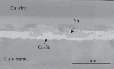
Figure 2 shows the initial Cu wire/Sn plating/Cu substrate joint interface. As previously discussed, we discovered that this is a mixture of regions where the Cu wire and Cu substrate are bonded only by the CuSn intermetallic compound and regions where they are bonded by the CuSn intermetallic compound and Sn. In order to be able to classify this bonding as bonding between the Cu wire and CuSn intermetallic compound or bonding between the Cu wire and Sn, we subjected each joint interface to detailed observations using TEM. Wefirst investigated the bonding state between the Cu wire and CuSn intermetallic compound.
Figure 3 shows observations in the vicinity of the joint at a location bonded only with the CuSn intermetallic compound; some types of cavities were locally found at the Cu wire/CuSn intermetallic compound interface and the CuSn intermetallic compound/Cu substrate interface. Only one kind of cavity was present at the Cu wire/CuSn intermetallic compound boundary located at the crystal grain boundaries, as shown in Fig. 4. It is conjectured that these were missed during the FIB processing (called ‘lacked grain’). In addition, other cavities seen along the bonding surface are thought to be non-attached regions where the Cu wire and CuSn intermetallic compound were unable to bond during the ultrasonic bonding (called ‘gaps’). Meanwhile, since the CuSn intermetallic compound/Cu substrate inter-face is formed before the ultrasonic bonding, it is assumed that the cavities, termed‘voids’, found at this interface do not originate in the ultrasonic bonding. These voids were formed
before the ultrasonic bonding because the tin plating process was reflow plating with heating.12)
Figures 5, 6 and 7 show the results of observations of the Cu wire/CuSn intermetallic compound interfaces. The crystal grains of the CuSn intermetallic compound are small at the bonding interface between the Cu wire and CuSn intermetallic compound, as shown in Fig. 5. Considering that 20µm
Surface of Sn plating
Cu wire
tool shape formed
20
µ
m
Fig. 1 SEM image of Cu wire bonding (52 degree tilted).
5µm Sn
Cu-Sn
Cu substrate Cu wire
Fig. 2 The cross-section result of SEM observation of the initial Cu wire/ Sn plating/Cu substrate joint interface.
A
Cu wire
Cu-Sn
Cu substrate 1µm
Lacked grain
Gap
Void
Fig. 3 The observation view in the vicinity of the joint at a location bonded only by the CuSn intermetallic compound.
B Cu wire
Cu-Sn
Initial interface
200nm Lacked grain
[image:2.595.307.547.71.217.2] [image:2.595.307.546.266.423.2] [image:2.595.308.547.471.652.2]Sn was present on the CuSn intermetallic compound before introducing the ultrasound, it is considered that the CuSn was nucleated during the growth process of the CuSn
intermetallic compound. The results of quantitative analysis of the Cu wire/CuSn intermetallic compound interface are shown in Table 1, and it is known that metallic bonding is accomplished at the bonding interface without the presence of oxidefilms of either Cu or Sn. It was also confirmed that the CuSn intermetallic compound at the bonding interface is Cu3Sn. It is apparent from the above discussion that bonding
at the Cu/CuSn intermetallic compound interface is metallic bonding of Cu and Cu3Sn.
3.2 Cu wire/CuSn intermetallic compound bonding state
Observations for the areas of Cu wire/Sn bonding and Cu wire/CuSn intermetallic compound bonding are shown in Fig. 8. The lines in Fig. 8 show the Sn/CuSn intermetallic compound interface and the CuSn intermetallic compound/ Cu substrate interface. According to Fig. 8, the majority of Sn crystal grains are 1 µm or greater in diameter, but the grains of the CuSn intermetallic compound are less than 1 µm in diameter, and the grain sizes are even finer, especially in the vicinity of the boundary with the Cu substrate. This is thought to be because the CuSn grains become finer as the CuSn intermetallic compound grows. In addition, gaps are seen at the interface between the Cu wire and Sn (upper left side of Fig. 8), because the shapes of the gaps follow the interface, and an approximately 10 nm layer was seen on the Sn-side of the gap; there is high probability that this is an area that did not attach during the ultrasonic bonding.
Figures 9 and 10 show the expanded views of a Cu wire/ Sn interface joint where a gap could not be confirmed. It was discovered from Fig. 9 that bonding between the Cu wire and Sn was accomplished with a thin intervening layer, the thickness of which was found to be approximately 10 to
Initial interface
C Cu wire
Cu-Sn
100nm
Fig. 5 The result of TEM observation between Cu wire and CuSn intermetallic compound (region B in Fig. 4).
Initial interface
D Cu wire
Cu-Sn
20nm
Fig. 6 The result of TEM observation between Cu wire and CuSn intermetallic compound (region C in Fig. 5).
Initial interface point 1
Cu point 2
point 3
Cu3Sn
Cu wire
Cu-Sn
5nm
[image:3.595.51.290.70.251.2]Fig. 7 The result of TEM observation between Cu wire and CuSn intermetallic compound (region D in Fig. 6).
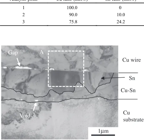
Table 1 Analysis data by EDX on spots 1 to 3 (Fig. 7).
Analysis point Cu ratio (mol%) Sn ratio (mol%)
1 100.0 0
2 90.0 10.0
3 75.8 24.2
A
Cu wire
Cu-Sn Sn
Cu substrate
1µm Gap
Void
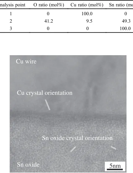
[image:3.595.305.548.94.331.2] [image:3.595.50.290.297.479.2] [image:3.595.50.290.525.708.2]80 nm from Fig. 10. Quantitative analysis was performed at the location shown in Fig. 11 to identify this layer. The analysis results are shown in Table 2. According to Table 2, Sn, O and Cu were confirmed from analysis point 2, where an oxide of Sn or Cu formed in a layer. From this, it became apparent that the Cu wire and Sn were bonded by means of the oxidefilm.
In ultrasonic bonding, the intermetallic bonding is believed to be accomplished by mechanically eliminating the oxide
films formed on the surfaces of the bodies being bonded by ultrasound and compression, and bringing into contact the fresh metallic surfaces exposed. However, our current observations indicate that Cu and Sn were bonded by the oxide film. Lattice images of the various bonding surfaces were observed to confirm the Cu wire/Sn oxidefilm and the Sn oxidefilm/Sn bonding states (Fig. 12, Fig. 13).
A distinct Cu crystal lattice on the Cu wire side was observed at the Cu wire/Sn oxide film interface (Fig. 12). The crystal lattice in the Sn oxide film was also observed, however, the long-range order of the crystal lattice was not as
long as that on the Cu wire side, and the lattice fringes were confirmed in multiple directions. There were a 3 nm widths layer in the vicinity of the bonding interface, but clear lattice fringe could not be confirmed, and it was found that the Cu wire and Sn oxidefilm were bonded without any defects such as cavities. It is assumed that the Cu wire and Sn oxidefilm were bonded at the bonding interface by the oxygen in the oxidefilm.
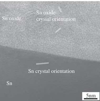
In the lattice image observations at the Sn oxidefilm/Sn interface (Fig. 13), lattice fringes were seen in multiple directions in the Sn oxide film, but no long-range order of B
Cu wire
Sn Gap
200nm
Fig. 9 The result of TEM observation between Cu wire and Sn (region A in Fig. 8).
C Cu wire
Sn
[image:4.595.331.520.68.259.2]100nm
Fig. 10 The result of TEM observation between Cu wire and Sn (region B in Fig. 9).
point2 Sn oxide
point3 Sn
D
E Cu wire
Sn
point1 Cu
20nm
[image:4.595.76.264.70.257.2]Fig. 11 The result of TEM observation between Cu wire and Sn (region C in Fig. 10).
Table 2 Analysis data by EDX on spots 1 to 3 (Fig. 11).
Analysis point O ratio (mol%) Cu ratio (mol%) Sn ratio (mol%)
1 0 100.0 0
2 41.2 9.5 49.3
3 0 0 100.0
Cu wire
Sn oxide crystal orientation
Sn oxide
Cu crystal orientation
5nm
[image:4.595.74.265.307.498.2] [image:4.595.317.532.323.602.2]any kind was observed. However, a Sn crystal lattice could be distinctly confirmed on the Sn side, and continuity was found to be high. In addition, unlike in the interface between the Cu wire and the Sn oxidefilm, no areas of contrast could be confirmed, nor were any cavities found in the vicinity of the interface. This is thought to be due to the differences in the bonding mechanism between the Sn oxide film and Sn and the bonding mechanism between the Cu wire and Sn oxide film. This Sn oxide film was formed by leaving the Sn exposed to air in the sample preparation process. Therefore, we assume that bonding at the interface between the Sn oxide film and the Sn as seen in Fig. 13 is due to bonding by oxygen, as in common metal oxide films. In addition, since this interface is formed without adding any external energy, it is thought that the Sn oxidefilm/Sn interface can also be distinctly confirmed. However, we assume that the areas of contrast were formed by forced bonding, since the interface between the Cu wire and Sn oxide film was formed by the ultrasound energy and compression during bonding.
In this investigation, we thus discovered that metals and oxidefilms could be locally bonded by ultrasonic bonding of Cu wire and Sn oxidefilm.
3.3 Bonding state at Cu wire/Sn interface
Figure 14 shows SEM observation of the joint cross-section after peel testing of the Cu wires bonded at 500 mW for 30 ms. This joint is the remaining joint at one end of a wire that was subjected to a peel test at 0.05 N, the other joint having been ruptured. From Fig. 14, it can be seen that though there were local Sn regions, the Cu wire was bonded to a CuSn intermetallic compound. In addition, voids were seen at the interface between the CuSn intermetallic compound and the Cu substrate, and cracks that developed in the peel test had advanced into the interface between the CuSn intermetallic compound and Cu wire or into the Sn.
Consequently, we were able to confirm that for Cu wire bonded to the Sn-plated Cu under these bonding conditions, residual Sn was locally present at the bonding interface
between the wire and Cu substrate, and bonding took place between the wire and the CuSn intermetallic compound.
4. Conclusion
The following conclusions were obtained with regard to the Cu wire bonding to a Sn-plated Cu substrate.
(1) Residual Sn exists locally at the initial bonding interface, and the locations bonded with interstitial Sn are intermixed with locations where the Cu wire is bonded with the CuSn intermetallic compound. (2) No oxidefilm layer was found at the bonding interface
in the joint between the Cu wire and the CuSn intermetallic compound, which TEM lattice images showed to be metallic bonding with Cu and Cu3Sn
being directly bonded.
(3) At locations where there was residual Sn, the Cu wire and Sn were bonded with an interstitial Sn oxidefilm, and there was a bonding area of indistinct crystal orientation of approximately 3 nm at the interface between the Cu wire and Sn oxidefilm.
(4) In ultrasonic bonding between Cu and Sn, the bonding was formed by the Sn oxide film.
Acknowledgments
The authors wish to thank Dr. M. S. Oliver, Dr. A. W. Hsing and Dr. T. S. Kim of Stanford University for their support in making specimens.
REFERENCES
1) D. Y. Shinand and P. J. Ficalora:IEEE Trans. Electron. Dev.26(1979) 2734.
2) S. Y. Yang, H. J. Byun, S. W. Park and W. J. Lee: Proc. 45th Annual on IEEE Reliability Physics Symposium, (2007) pp. 113116.
Sn oxide
Sn
Sn crystal orientation Sn oxide
crystal orientation
[image:5.595.74.264.69.261.2]5nm
Fig. 13 The result of TEM observation between Cu wire and Sn (region E in Fig. 11).
Cu wire
Cu-Sn
Cu substrate Crack by peel testing
Sn
Void
1µm
1
µ
[image:5.595.306.546.69.307.2]m
3) H. S. Chang, K. C. Hsieh, T. Martens and A. Yang: IEEE Trans. Compon. Packag. Tech.27(2004) 155160.
4) K. Toyozawa, K. Fujita, S. Minamide and T. Maeda: IEEE Trans. Compon. Hybrids Manuf. Tech.13(1990) 667672.
5) J. Schwizer, M. Mayer, D. Bolliger, O. Paul and H. Baltes: The 24th IEEE/CPMT Symposium on Electronics Manufacturing Technology Symposium, (Austin, USA, 1999) pp. 108114.
6) S. Koyama, M. Takahashi and K. Ikeuchi:Solid State Ion.172(2004) 397401.
7) M. Onishi and H. Fujibuchi: Trans. Jpn. Inst. Met.16 (1975) 539 548.
8) I. Shohji, T. Sakurai and S. Arai:Key Eng. Mater.297300(2005) 28192824.
9) H. Xu, C. Liu, V. V. Silberschmidt and H. Wang: The 58th Electronic Components and Technology Conference, (Florida, USA, 2008) pp. 14241430.
10) H. Clauberg, B. Chylak, N. Wong, J. Yeung and E. Milke: IEEE CPMT Symposium Japan, (Tokyo, Japan, 2010) pp. 14.
11) M. Maeda, T. Sato, N. Inoue, D. Yagi and Y. Takahashi:Microelectron. Reliab.51(2011) 130136.