A Simple Model to Describe the Rule of Glancing Angle Deposition
Qin Zhou, Zhengcao Li
*, Jie Ni and Zhengjun Zhang
Advanced Materials Laboratory, Department of Materials Science and Engineering, Tsinghua University, Beijing 100084, P. R. China
A model was built to study the rule of glancing angle deposition. This model, which is called hemisphere model, is convenient to describe how the experimental conditions influence morphology of the nanostructures prepared by GLAD. Influence of experiment conditions such as incidence angle, incidence rate, substrate temperature, and substrate rotation rate are theoretical analyzed by the hemisphere model, and validated respectively by amount of experiments. As an application of the model, metals of different melting points were deposited into coherent multi-section nanorods by adjusting substrate temperature. [doi:10.2320/matertrans.M2010342]
(Received September 29, 2010; Accepted December 8, 2010; Published February 2, 2011)
Keywords: model, glancing angle deposition, hemisphere growth
Glancing angle deposition (GLAD) is a physical vapor deposition method which the trajectory of incident vapor flux is not parallel to the substrate normal, but depositing at oblique angles. K. Robbie and M. J. Brett had carried out this method,1,2)and then M. M. Hawkeye and M. J. Brett analyzed
the deposition mechanism.3–5)
GLAD technique is a simple but powerful means which is capable of producing thin films with pre-designed nano-structures such as nanopillars, slanted posts, zigzag columns, spirals, etc.6–8)These nanostructures can be used in a variety of fields, e.g., photonic crystals, magnetic storage media, and optoelectronic devices, etc.9–14) For example, arrays of Ag nanorods can be used as surface-enhanced Raman scattering substrates, and Rhodamine 6G molecules can be detected to a concentration limit of 1014mol/L by this substrate.15,16)
Arrays of HfO2 nanocolumns can be used as antireflection
coating, and the antireflection rate can be adjust by GLAD conditions.17)
In this letter, we report our effort to build a simple model which is called hemisphere growth model to study the rule of glancing angle deposition. Influence of experiment conditions such as incidence angle, incidence rate, substrate temperature, and substrate rotation rate are theoretical analyzed by the hemisphere growth model, and validated respectively by amount of experiment. As an application of the model, metals of different melting point were deposited into coherent multi-section nanorods by adjusting substrate temperature.
When deposition at oblique angles, after nucleation and initial growth, columns format following the structure zone model.3,5) According to the structure zone model, when
substrate temperature is lower than 0.3 melting point of target material, the film microstructure is composed of tapered columns with domed tops, and GLAD principally relies on these structures. On the basis of this, we build a model that incident vapor flux nucleates on the substrates and grows into close-packing hemispheres, and in GLAD process nano-structures grow from these hemispheres.
It is well known that atomic shadowing and adatom diffusion are the dominate growth mechanisms in GLAD. When depositing at oblique angles, one hemisphere will form
a shadow to nearby hemispheres as shown in Fig. 1. The diameterDof hemispheres is related to the temperature of the substrates when they form and the melting point of the material. The diameter increases when the temperature becomes higher, while decreases when the melting point of the material becomes higher.3,5)
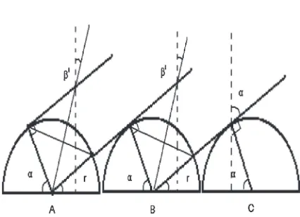
When depositing at incident angle , hemisphere B will form a shadow area0 to hemisphere A, and satisfies following formula:
¼arccosð2 cos1Þ
Hemisphere A will form a shadow areato itself, and incident vapor flux can deposit from to . The incident beam flux of unit area atarc angle dispersed to a area ofsinðÞon the hemisphere, thusdarc length gainssinðÞdmaterial beam flux, and total material on the arc is RsinðÞd. If atomic diffusion is abundant from to , nanorods growth angle will satisfies from average from to , as following formula:
¼ Z
sinðÞd Z
sinðÞd
¼þcosðþÞ sinðþÞ
2 cos
Fig. 1 A schematic of the hemisphere growth model.
*Corresponding author, E-mail: [email protected]
Materials Transactions, Vol. 52, No. 3 (2011) pp. 469 to 473
[image:1.595.319.532.272.426.2]But if atomic diffusion is low, growth angle will approach to . Actual growth angle will between and . We introduced a parameterkto simulate actual growth angle:
¼ ð1kÞþk
A similar but simpler formula is:
¼karccosð2 cos1Þ
2
Growth proportionwhich means grown area to total area is also a function of incident angle . The experimental is calculated from top view SEM image of the nanorod films, which is area of rods divided by area of total area. The calculated is calculated from projective area of arc from angle to angledivided by projective area of hemisphere in Fig. 1.
¼cosðÞ þcosðÞ
2
¼cosðÞ
2 þ
cosðarccosð2 cos1Þ Þ
2
We define growth ratio as the nanorod length growth speed, and incident ratioas incident flux depositing speed. Growth ratio is not the same as incident ratio, but a function of incident angleand incident ratio:
¼cos=cos
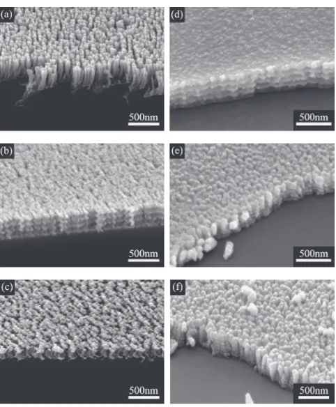
The aforementioned formulas are mainly about how incident angle affects the grown morphology. A series of experiments were performed to validate these simulations. Figure 2 shows the morphology of Fe thin films prepared
by GLAD with different incident angles. The SEM micro-graphs were taken with a FEI SEM (QUANTA 200FEG) working at 20 kV. The Fe thin films shown in Fig. 2(a), (b), (c), (d) and (e) were deposited with incident angle of 74,
78, 82, 85 and 88, respectively. The other deposition
parameters were totally the same. The system was pumped down to a vacuum level of8105Pa, and the films were
deposited at a depositing rate is 0.3 nm/s, with the thickness monitored by a quartz crystal microbalance. When incident angles were adjusted from 74 to 88, the growth angles
[image:2.595.48.292.71.359.2]became larger, the Fe nanorods grew shorter, and the porosity turned larger.
Figure 3 shows a comparison between the results simu-lated by the hemisphere model and Fe films prepared in our experiments. Figure 3(a), (b) and (c) show how growth angle
Fig. 2 The SEM images of Fe thin films prepared by GLAD with different incident angles. (a) at 74; (b) at 78; (c) at 82; (d) at 85; (e) at 88.
[image:2.595.326.523.76.532.2] [image:2.595.84.256.614.662.2], growth proportion and growth ratio change while incident angle turns from 1 to 89, respectively.
Experimental growth angleand growth ratio are achieved from cross-section view SEM image by statistic tilting angle and nanorod length. Growth ratio is calculated from that nanorod length divided by growth time. Experimental growth proportionis calculated from top view SEM image of the nanorod films, which is area of rods divided by area of total area. As in our experiment, the flux incident ratio and growth time is the same, thus the experimental = of different incident angle is in the same trend as rod length. And experimental =is plot from rod length with different incident angle. When deposited at oblique angles (7090),
the simulation accorded with the experimental results. For this model is used for glancing angle deposition, which is a method when incident angle is larger (>70), we didn’t achieve the experimental data when the oblique angle is smaller than 70.
The increase of beta and decrease of growth proportion as a function of alpha angle are intuitively understandable. The growth ratio of columns increases slowly to a maximum at about 70 angle and then rapidly decreases as angle
increases. As angle increases, the nanorods growth area decreases (where parameter 1= comes from), which leads growth ratio increases asangle increases. Therefore, as
angle increases, incident beam flux from the same area disperses to larger area on the substrate (where parameter
cos=coscomes from), which leads growth ratio decreases as angle increases, especially at larger angle. That’s why the growth ratio decreases rapidly asangle increases when
angle is larger than 70.
The forementioned Fe films are deposited without sub-strate rotation, when deposited with an angular velocity !, the nanostructures will become no longer tilted nanorods, but helical or vertical columns.
Growth angle , growth ratio and substrate angular velocity!effect the deposition morphology. SupposeX,Y,Z
is a rectangular coordinate system, and axis Z is vertical to the substrate, while axis X is parallel to the initial growth direction, axis Y is perpendicular to the initial growth direction. After deposited a period of timet, the growth track becomes (X,Y,Z):
X¼ =!sinsin!t
Y¼ =!sinð1cos!tÞ
Z¼ tcos
It is a helical morphology. Suppose the radius of the helix is
R, and screw pitch isH:
R¼ =!sin¼=!cos=cossin
H¼2 =!cos¼2=!cos=cos2
For and are functions of incident angle , we define
FrðÞ ¼cos=cossin and FhðÞ ¼cos=cos2 to
simplify the expression. Both of Fr() and Fh() are also the functions of incident angle.
Suppose the diameter of the nanorods is, which is a direct propagation of hemisphere diameter D. When H> , the morphology will be helix, otherwise will be columns. Thus, to achieve helical nanostrustures, one should choose deposition parameter!slow enough:
! <2cos=
As a simulation result, =! determines the deposited morphology as one parameter, and if=! is the same, the morphology is similar;17) When the other parameters are
definite, small!induces helical morphology; largerresults in smaller R and smallerH, thus nanohelixes will be more discrete with each other.
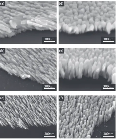
Figure 4 shows the morphology of Fe thin films prepared by GLAD with different substrate angular velocity and different incident angles at room temperature. Figure 4(a), (b) and (c) show the Fe films deposited at substrate angular velocity was 2 rpm, 0.25 rpm and 0.05 rpm, respectively, while other parameters were the same. When the angular velocity was 2 rpm, the morphology of the Fe film was vertical nanocolumns; when the angular velocity was 0.25 rpm, the morphology turned into nanohelixes; when the angular velocity was 0.05 rpm, the screw pitch H was bigger than that was when!was 0.25 rpm. Figure 4(d), (e) and (f) show the Fe films deposited while incident angles were 65, 75and 85, respectively. When the incident angle
was 65, the radius of the helixRwas so big that helixes were
connected with each other, and the screw pitch Hwas big, too, thus the Fe films in Fig. 4(d) looks like multilayer films. When the incident angle was 85, the radius of the helixR
was small enough to apart from each other, and the screw
[image:3.595.307.548.68.360.2]pitch H was small, too, therefore, helical nanostructures formed.
Figure 5 shows a comparison between the simulation results and Fe films prepared in our experiments. Figure 5(a) and (b) show how radius of the helixR(FrðÞ ¼R!=) and
screw pitch H (FhðÞ ¼H!=2) change while incident
angleturns from 1 to 89, respectively. When deposited
at oblique angles (7090), the simulation accorded with
the experimental results. Growth angle increases as
angle increases, the vertical part of growth decreases while horizontal part increases, thus screw pitch Hdecreases and radius of the helixRincreases whenangle is smaller than 70. When angle is larger than 70, the growth ratio
decreases rapidly, so both radius of the helix R and screw pitchHdecreases.
Besides atomic shadowing, adatom diffusion is one of the dominate growth mechanisms in GLAD, too. According to Fick’s law, diffusion coefficientDfollows:
D/expðEd=kbTsÞ
Here Ed means diffusion energy, kb means the Boltzmann
constant and Ts means the temperature of substrate. Thus,
temperature of substrate Ts effects diffusion coefficient
greatly, high substrate temperature results in large diffusion coefficient. In addition, according to the structure zone model, after nucleation and initial growth, the size of tapered columns depends on the substrate temperature. As a result,
the size of hemisphere in the hemisphere growth model depends on the substrate temperature Ts. Therefore, low
substrate temperature induces thin and separated nanostruc-tures, while high substrate temperature induces thick and connected nanostructures.18)
Figure 6 shows the morphology of Ag thin films prepared by GLAD with different substrate temperature. The Ag thin films shown in Fig. 6(a), (b) and (c) were deposited without substrate rotation, and at substrate temperature of room temperature, 10C and 40C, respectively. Figure 6(d), (e) and (f) show the Ag thin films deposited with angular velocity of 2 rpm, and at substrate temperature of room temperature, 10C and 40C, respectively. The system
was pumped down to a vacuum level of3105Pa, and the
films were deposited at a depositing rate is 0.5 nm/s, with the thickness monitored by a quartz crystal microbalance. Both with and without substrate rotation, the Ag nanostructures deposited at room temperature are connected, while at
40C are separated and porous.
As an application of the hemisphere growth model, metals of different melting point were deposited into coherent multi-section nanorods by adjusting substrate temperature. Metals of different melting point have different diffusion coefficient, so when they are deposited into multi-section nanorods, they will have different nanorod radius. In the hemisphere growth model, the diameter of the nanorodsis a direct propagation of hemisphere diameter D, andDincreases when substrate
Fig. 6 The SEM images of Ag thin films prepared by GLAD at incident angle of 85with different substrate temperature. (a) deposited without substrate rotation and at room temperature; (b) deposited without substrate rotation and at10C; (c) deposited without substrate rotation and at
40C; (d) deposited with angular velocity of 2 rpm and at room temperature; (e) deposited with angular velocity of 2 rpm and at10C; (f) deposited with angular velocity of 2 rpm and at40C.
[image:4.595.65.271.69.398.2] [image:4.595.307.548.71.361.2]temperature rises or melting point of material becomes lower. Thus in order to depositing coherent multi-section nanorods with different melting point materials, one should deposit high melting point material in high substrate temperature and low melting point material in low temperature. Figure 7 shows the Fe-Ag thin films prepared by GLAD with different substrate temperature. We use liquid nitrogen to control the substrate temperature. Substrates and liquid nitrogen contain-er are connected with a coppcontain-er belt, which transfcontain-ers heat from substrates to liquid nitrogen. A k style thermocouple is used to measure the temperature of substrates. The Fe-Ag nano-structures in Fig. 7(a) were deposited at room temperature,
and the Fe (bulk melting point is 1535C) nanorods are separated but the Ag (bulk melting point is 960C) nanorods
are connected to each other; the ones in Fig. 7(b) were deposited at40C, and the Ag nanorods are separated but
the Fe nanorods become very thin that two or three Fe rods connect to one Ag rod; the nanostructures in Fig. 7(c) were deposited at room temperature while depositing Fe and at
40C while depositing Ag, and the multi-section nanorods
are coherent.
In summary, we have built a simple model which is called hemisphere growth model to study the rule of glancing angle deposition. Influence of experiment conditions such as incidence angle, incidence rate, substrate temperature, and substrate rotation rate are theoretical analyzed and simulated by the hemisphere growth model, and validated respectively by amount of experiment. As an application of the model, metals of different melting point were deposited into coherent multi-section nanorods by adjusting substrate temperature. This study provides a simple way to realize the rule of glancing angle deposition, and help to achieve different morphologies by adjusting experiment conditions of GLAD.
Acknowledgments
The authors are grateful to the financial support by the National Natural Science Foundation of China (50931002 and 61076003), and the National Basic Research Program of China (973 program, 2007CB936601 and 2010CB731600).
REFERENCES
1) K. Robbie, L. J. Friedrich, S. K. Dew, T. Smy and M. J. Brett: J. Vac. Sci. Technol. A13(1995) 1032–1035.
2) K. Robbie and M. J. Brett: J. Vac. Sci. Technol. A15(1997) 1460– 1465.
3) Matthew M. Hawkeye and Michael J. Brett: J. Vac. Sci. Technol. A25
(2007) 1317–1335.
4) Cristina Buzea, a Kate Kaminska, Gisia Beydaghyan, Tim Brown, Chelsea Elliott, Cory Dean and Kevin Robbie: J. Vac. Sci. Technol. B
23(2005) 2545–2552.
5) H. T. G. Hentzell, C. R. M. Grovenor and D. A. Smith: J. Vac. Sci. Technol. A2(1984) 218–219.
6) M. Malac, R. F. Egerton, M. J. Brett and B. Dick: J. Vac. Sci. Technol. B17(1999) 2671.
7) M. Malac and R. F. Egerton: J. Vac. Sci. Technol. A19(2001) 158. 8) B. Dick and M. J. Brett: J. Vac. Sci. Technol. B21(2003) 23. 9) S. R. Kennedy, M. J. Brett, H. Miguez, O. Toader and S. John:
Photonics Nanostructures1(2003) 37.
10) B. Dick, M. J. Brett, T. J. Smy, M. R. Freeman, M. Malac and R. F. Egerton: J. Vac. Sci. Technol. A18(2000) 1838.
11) H. Alouach, H. Fujiwara and G. J. Mankey: J. Vac. Sci. Technol. A23
(2005) 1046.
12) J. P. Singh, F. Tang, T. Karabacak, T. M. Lu and G. C. Wang: J. Vac. Sci. Technol. B22(2004) 1048.
13) A. Lakhtakia: Mater. Sci. Eng. C19(2002) 427.
14) M. M. HawKeye and M. J. Brett: J. Vac. Sci. Technol. A25(2007) 1317.
15) Ralph A. Tripp, Richard A. Dluhy and Yiping Zhao: Nanotoday 3
(2008) 31–37.
16) S. B. Chaney, S. Shanmukh, R. A. Dluhy and Y.-P. Zhao: Appl. Phys. Lett.87(2005) 031908.
17) N. Jie, Z. Yu, Z. Qin and Z. Zhengjun: J. Am. Ceram. Soc.91(2008) (10) 3458–3460.
18) C. M. Zhou and D. Gall: J. Vac. Sci. Technol. A25(2007) 312–318. Fig. 7 The SEM images of Fe-Ag thin films prepared by GLAD with
different substrate temperature. (a) deposited at room temperature; (b) deposited at40C; (c) deposit Fe at room temperature and Ag at40C.
[image:5.595.60.279.61.585.2]