Enhanced Mechanical Properties of LaF
3Thin Films by Ion Plating Deposition
Takanobu Hori
1;2;*, Shinji Motokoshi
3and Hiroshi Kajiyama
2 1Research & Development Management Division, ShinMaywa Industries, Ltd., Takarazuka 665-8550, Japan
2Department of Semiconductor Electronics and Integration Science, Graduate School of Advanced Sciences of Matter, Hiroshima University, Higashi-Hiroshima 739-8530, Japan
3Institute for Laser Technology, Osaka 550-0004, Japan
The mechanical properties of lanthanum fluoride (LaF3) films are investigated. The films are deposited by using a resistive heating (RH)
boat evaporation method and the advanced ion plating (AIP) method. A severe abrasion resistance test and a laser induced damage threshold (LIDT) test are done on the films. Abrasion resistance is increased by increasing the deposition temperatures for RH films. On the other hand, for AIP films, abrasion resistance is increased by adding direct current (DC) bias voltage. It is confirmed that the AIP films have a superior LIDT characteristics than those of RH films. With an additional DC bias voltage superimposed to a self bias voltage, the abrasion resistance and LIDT value is further improved. Based on the proposed mechanism of LIDT process, the microstructures of LaF3films are discussed.
[doi:10.2320/matertrans.M2010367]
(Received March 7, 2011; Accepted April 21, 2011; Published June 8, 2011)
Keywords: antireflective coating, lanthanum fluoride, ion plating, abrasion resistance, laser resistance
1. Introduction
Antireflective (AR) coating is indispensable to all kinds of optical devices to reduce optical loss due to the discontinuity of refractive index (n) at the interface. Usually, the thin films of high and low n materials are alternatively deposited at the surface of optical devices. By the combination of higher and lowernmaterials, lower reflection at wider wavelength region could be obtained.
Lanthanum fluoride (LaF3) is known to be a high n
material which is effective for the wavelengths from vacuum ultraviolet to visible light. The most importance ultraviolet optical device is a laser. Therefore, the laser resistance of LaF3 AR coating is quite important as well as abrasion
resistance, environmental stability.
LaF3 films have been conventionally prepared by using a
resistive heating (RH) method, where thermally evaporated materials are deposited on a heated substrate. It has been reported that the laser resistance of RH film was improved by RH deposition.1)However, aging and thermal reliabilities are still quite low because of columnar structures and grain boundaries.
Ion plating (IP),2) ion assist deposition (IAD)3) and ion
beam sputtering (IBS)4) were applied to get dense packed
uniform films with less columnar structures and grain boundaries. Among the above methods, we will focus on the IP method. In a conventional IP method, evaporated species are excited by plasma. A self bias voltage is naturally formed between a plasma and a floated substrate holder. Crystal growth by a conventional IP deposition is enhanced, because ionized evaporated species are accelerated towards a substrate by such a self bias voltage. In this study, we use the advanced ion plating method5–8)we have developed, in which an external direct current (DC) bias voltage could be additionally applied to a substrate holder. By using the advanced IP (AIP) method, it becomes possible to control the
crystal growth by changing the kinetic energy of impinging species from a plasma region.
In this paper, we compare the film properties deposited by RH method and AIP method in term of film morphology, crystallinity, abrasion resistance, laser resistance. The effects of the AIP conditions on film characteristics are discussed.
2. Experimentals
Figure 1 shows a schematic diagram of the AIP deposition system ShinMaywa Industries, Ltd. has developed for this study.5–8)A radio frequency (RF: 13.56 MHz) power and an
external DC bias voltage (VDC) are applied to a substrate
holder through a matching box (MB) at the same time. Since the capacitance between a substrate holder and a chamber was considerably smaller compared with the matching capacitance, RF plasma could be sustained at the vacuum pressures as low as103Pa, which is 10 times lower pressure than that of a conventional RF-IP method. So, we can reduce the contaminants in films. The substrate holder is insulated from chamber that is ground by the capacitor in MB. Therefore, the self bias is impressed to the substrate holder (and the substrate) when plasma is generated. The difference from a conventional RH evaporation is an applied RF power for plasma generation and a DC bias voltage for changing the impinging velocity.
Deposition conditions were as follows both for RH and AIP films. The base pressure of chamber was1:33103Pa
or less, and the LaF3 granules (purity: 99.9 mass%) was
evaporated by resistance heating of a tungsten boat. LaF3 film with a thickness of 300 nm was deposited on a
silica glass substrate (diameter: 30 mm, root mean square roughness: 0.6 nm or less). Deposition rate was 1 nm/s and substrate temperature (Ts) was 25C (RH, AIP), 150C (RH)
and 300C (RH). In AIP deposition, a RF power of 300 W and 700 W were applied. Also, a DC bias voltage of
700V were superimposed to a self bias voltage of typically
150V.
The film crystallinity was measured by X-ray diffraction (XRD; Rigaku RAD-2C) with2scanning at a fixed incident angle, and calculation of the grain size. The monochromatic X-ray of CoK1radiation (¼0:17889nm) was used. The grain sizeDwas calculated by the Scherrer’s equation.
D¼K=cos
where K is the Scherrer’s constant, is the X-ray wave-length,is the Bragg diffraction angle, andis the full width of peak at half maximum intensity.
The surface morphology was measured by atomic force microscope (AFM; JEOL JSPM-5400). The RMS was calculated. The cross-sectional images was measured by a field emission scanning electron microscope (SEM; Hitachi S-4800).
Abrasion resistance was measured by rubbing film surface with a steel wool (#0000; extra fine) mounted on a holder with a surface area of 1 cm2, as shown in Fig. 2. The abrasion
condition was based on the U.S. Department of Defense standard (Mil-C-14806A). Film surface was rubbed by a loaded steel wool by 20 times. After rubbing, the surface was checked by an optical microscope whether there are any physical damages or peeling.
The laser resistance was evaluated by detecting the morphological change induced by a laser irradiation. The experimental setup is exhibited in Fig. 3. A Q-switched Nd:YAG laser system (Spectra Physics Co. Quanta-ray) with 10 ns pulse width at 1064 nm was used. The laser pulse of a single mode oscillator was amplified by amplifier and it converted into the 355 nm wavelength by two KDP
(KH2PO4) crystals. The laser pulse was guided to a focusing
lens with 3000 mm focal length. The pulse width was measured by a biplanar photo tube, and the energy of each pulse was measured by a energy meter. The energy of irradiation laser beam was adjusted with a polarizer and half wave plate (HWP). Beam profile and spot size were measured with a CCD camera, which was installed at the equal distance from the lens to the sample surface.
Laser induced damage test was performed by a 1-on-1 method,9)in which the laser focused point were changed by every laser shot. The surface after laser shot irradiation was observed using Normarski microscope at50magnification. Laser induced damage threshold (LIDT) was determined at the maximum peak fluence of Gaussian distribution of laser energy that does not caused a damage.
3. Results and Discussion
3.1 X-ray diffraction (XRD) results
Figure 4 shows the XRD patterns of the films prepared by a RH method at differentTs. It is obvious that the films are
polycrystalline. The peaks of polycrystalline films matched well with hexagonal structure of LaF3(JCPDS 00-032-0483).
The diffraction peaks of (111) and others were measured. Figure 4 shows that the preferred crystal orientation changed withTs. By increasing the Ts, the intensity of the strongest
peak becomes larger, and the peak has changed from (110) to (111).
Table 1 shows the grain size calculated by the profiles of (111) peak. The grain size were 9.2 nm and 24.0 nm atTsof Test piece
20 strokes Load
Steel wool (#0000)
Fig. 2 Schematic diagram of a severe abrasion tester.
Energy meter
CCD camera
Biplanar Microscopy
Polarizer
HWP Lens
f=3000
Osc.
Nd:YAG 1064nm 10ns 10Hz
Pulse selector, shaper & Amp.
Sample stage Rotation
stage
Fig. 3 Experimental setup of laser induced damage testing.
Ar
MB RF
DC
Vacuum pump Substrate holder
Thickness monitor Substrate
Resistance heating boat Heater
LaF3
Plasma 650mm
Fig. 1 Schematic diagram of the ion plating.
0 250 500 750 1000 1250 1500 1750
10° 20° 30° 40° 50° 60° 70° 80° 90° 100°
Intensity (arb.unit)
2θ
11
0
111
11
2
300 11
3
302 221
223 304 11
5
41
1
25°C 150°C 300°C
(a) (b) (c)
Fig. 4 X-ray diffraction patterns of LaF3 films prepared at different
[image:2.595.307.542.71.187.2] [image:2.595.59.275.72.214.2] [image:2.595.319.535.245.367.2] [image:2.595.94.244.262.389.2]25C and 300C, respectively. It is clear that grain sizes were
increased by increasing Ts. G. Liu et al. also reported the
similar dependence of the grain size of LaF3 film on the Ts
in the case of electron beam evaporation deposition.10)This
is indicating that crystal growth was promoted at higherTs.
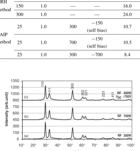
Figure 5 shows the XRD patterns of films prepared by AIP method. The peak pattern was similar with the RH film deposited at 25C shown in Fig. 4(a). The film had a
pollycrystalline structure. It was confirmed that a DC bias voltage reduced grain size at the RF power of 300 W: Grain size was be 8.4 nm and 10.7 nm with and without a DC bias voltage, respectively. This shows that the large crystal growth was suppressed by the effect of the ion bombardment.
3.2 Root mean square roughness (RMS)
RMS measurement listed in Table 2. It seemed to resemble the value of RMS and grain size that was shown in Table 1. In RH films, RMS became larger by increasing Ts. The
crystal growth advanced by the heat energy after an evaporated particle reaches the substrate, and it seemed to roughen according to the shadow effect, since the grain size increases. In AIP films, RMS less depended on the RF power and DC bias.
3.3 Cross-sectional images
Figure 6 shows the cross-sectional SEM images of the films. It is obvious that the films are columnar structures. In RH films, it is clear that crystal grew by increasingTs. The
diameter of the columnar structures were about 10 nm and
about 30 nm at Ts of 25C and 300C, respectively. In AIP
films, crystal growth was done not so well. The surface morphology and the diameter of the columnar structures were also same as in Fig. 6(a).
Thus, the grain size values estimated from the Scherrer’s equation in the subsection 3.1 were verified with those observed in SEM.
[image:3.595.47.289.84.215.2]3.4 Abrasion resistance
Table 2 shows the degree of the abrasion injury as an intercomparison. The symbol ‘‘ ’’ in the table is shown that a film was not peeled off at load of 3.9 N. ‘‘ ’’ is shown that film was scratched at 2.9 N, and, ‘‘’’ is shown that film was scratched at 2.0 N. And, ‘‘’’ is shown that film was peeled off all at 4.9 N. Still, Fig. 7 shows the surface microscope images after the test at 4.9 N.
For RH films, abrasion resistance increased by increasing
Ts. For example, peeling was not identified at 3.9 N atTsof
300C. For AIP films deposited withoutV
DC, the abrasion
resistance is slightly improved compared with RH film atTs
of 25C. But, it showed poor abrasion resistance. Linear
scratches were observed, and density of linear scratches increased by increasing the load.
We focus on the effect of superimposed VDC on the
abrasion resistance of AIP film at Ts of 25C. The abrasion
resistance was drastically increased by applying a VDC as
shown in Table 2. We propose the mechanism of improved abrasion resistance. In the AIP method, evaporated LaF3
clusters are excited not only to the ionized states but also to excited neutral states by Ar plasma. Furthermore, the ionized species gain extra kinetic energies by aVDC. These excited
species definitely contribute to the crystal growth: the surface migration and nucleation are promoted. Ion bombardment suppresses crystal growth, and, a minute and packed film is formed. Our result shows that such kinetic energy gains are the key to improve the abrasion resistance of LaF3 films.
3.5 Laser induced damage threshold (LIDT)
The results of LIDT measurements are listed in Table 2. For RH films, clearTsdependence was not observed and the
values were between 3.5–4.2 J/cm2. This is a quite contrast to the abrasion resistance discussed in the former section: It increased by increasingTs. For RH films, the LIDT values
were higher than those of RH films in the range of 5.5–
Table 1 Grain size calculated by (111) peak of LaF3thin films.
Ts (C)
Deposition rate (nm/s)
RF power (W)
DC bias (V)
(111) Grain size (nm)
RH 25 1.0 — — 9.2
method 150 1.0 — — 16.0
300 1.0 — — 24.0
25 1.0 300 150 10.7
(self bias) AIP
25 1.0 700 150 10.5
method
(self bias)
25 1.0 300 700 8.4
0 150 300 450 600 750 900 1050 1200 1350
10° 20° 30° 40° 50° 60° 70° 80° 90° 100°
Intensity (arb.unit)
2θ
11
0
111
300
302 221 223 411
RF 300W RF 700W RF 300W VDC−−700V
(a) (b) (c)
Fig. 5 X-ray diffraction patterns of LaF3films prepared by AIP deposition
[image:3.595.303.550.95.232.2] [image:3.595.55.283.120.366.2]at (a) RF 300 W withoutVDC; (b) RF 700 W withoutVDC; (c) RF 300 W withVDCof700V.
Table 2 RMS, abrasion resistance and LIDT of LaF3 thin films. (RMS:
root mean square roughness, LIDT: laser induce damage threshold)
Ts (C)
Deposition rate (nm/s)
RF power
(W)
DC bias (V)
RMS (nm)
Abrasion resistance
LIDT (J/cm2)
RH 25 1.0 — — 1.4
4.2
method 150 1.0 — — 2.8 3.5
300 1.0 — — 4.9 4.1
AIP
25 1.0 300 150
(self bias) 1.7 5.5
method 25 1.0 700 150
(self bias) 1.6 5.6
100
μ
m
100
μ
m
100
μ
m
100
μ
m
(a)
(b)
(c)
(d)
peeling
peeling
Fig. 7 Surface microscope image of LaF3thin films after severe abrasion test at load of 4.9 N. Samples prepared by (a) RH deposition at
25C; (b) RH deposition at 300C; (c) AIP deposition at RF 300 W withoutV
DC; (d) AIP deposition at RF 300 W withVDCof700V.
(a)
(b)
(c)
(d)
300nm
300nm
300nm
300nm
Fig. 6 Cross-sectional SEM images of LaF3films. (a) RH deposition at 25C; (b) RH deposition at 300C; (c) AIP deposition at RF 300 W
[image:4.595.70.526.72.420.2] [image:4.595.106.487.476.760.2]6.7 J/cm2. Laser damage resistance of LaF
3 thin films have
been reported in the previous literatures.1,10) H. Yu et al.
studied about characterization of LaF3 coatings prepared at
different temperatures and rates. In their study, LIDT measurement was approximately 4–7 J/cm2. Then, G. Liu
et al. studied films prepared by EB method and LIDT
measurement was about 1.5–4 J/cm2. These results are
equivalent to our results of RH films on similar conditions (Ts: 300C, deposition rate: 1.0 nm/s). On the other hand,
LIDTs of AIP films are shown above already. This results show that the AIP method is available technique for improvement of laser resistance. Furthermore, a DC bias voltage (700V) of superimposed to a self bias voltage obviously improved both the abrasion resistance and LIDT.
The mechanism of LIDT process occurring in the thin film under laser irradiation has been discussed based on the phenomenological modes in term of thermal destruction11)
and dielectric breakdown.12,13) The thermal destruction is
caused by thermal expansion due to the absorption of laser photons. In the dielectric breakdown model, films are broken by electron avalanche.14)The electrons emitted from defects
and/or impurities are accelerated by the electric field of laser photons.15,16) Those high energetic electrons could ionize atoms, or excite defects and/or impurity sites. In the results, conduction electrons are generated. By the repetition of these processes, the number of conduction electrons is nonlinearly increased. This is an avalanche effects occurring in the film under laser irradiation. Because of the electric field induced by electron avalanche, films are destructed electrically at the critical number of avalanche electrons.
In the LIDT measurement in this study, pulsed laser photons are irradiated on to the sample: pulse duration: 2 ns, wavelength: 355 nm, frequency: 10 Hz. The band gap energy of LaF3is 9.7 eV. Therefore, the thermal destruction model is
hard to take in this study. It should be pointed out that abrasion resistance and LIDT prove the different aspects of crystallinity of the LaF3films in this study. By increasingTs,
abrasion resistance increased. As for LIDT, it has not shown an obvious dependence onTs. In the case of AIP films which
were deposited without a DC bias voltage superimposed to a self bias voltage, the abrasion resistance was measured to be poor, although the LIDT were all higher that those of RH films.
The basic mechanism of the enhanced mechanical proper-ties is likely as follows. A superimposed DC bias voltage accelerates the impinging LaF3þ ions towards the
sub-strate.17) Those impinging ions with higher kinetic energy
enhance surface migration. They also reduce grain sizes because of ion bombardment at the growth front as shown in Table 2. The AIP films could have smaller sizes of grains, leading to a dense packed crystal structure. So, it might be plausible to consider that the number of initial electrons for avalanche amplification, since the number of defects would be reduced in the AIP films.
4. Conclusion
LaF3 films were synthesized by using a resistive heating
(RH) evaporation method and the advanced ion plating (AIP) method. The effects of a substrate temperature (Ts), an input
RF power and a DC bias voltage on the mechanical properties were measured in term of abrasion resistance and laser induced damage threshold (LIDT) as well as a grain size and surface roughness.
The grain size of AIP films was reduced by a DC bias voltage superimposed to a self bias voltage of typically
150V. Since the ion bombardment was enhanced by a DC bias voltage, the grain sizes and a surface roughness were reduced so much in the case of AIP deposition.
The LIDT values were in the range of 5.5–6.7 J/cm2. This is higher than those of RH films. LIDT is the threshold laser power for dielectric breakdown induced by avalanche electrons emitted from defects and/or impurities. Thus, the higher LIDT value reflects the lower density of defects and/or impurities in the film. So, it is reasonable to consider that, in the AIP deposition, the crystallinity of LaF3 film
was enhanced by the accelerated impinging LaF3þ ions by
superimposing a DC bias voltage. It is noted that the most excellent abrasion resistance and the highest LIDT value were only realized by the ion plating deposition with a DC bias voltage super imposed to a self bias voltage.
Based on the above results and discussions, it was confirmed that mechanical properties of LaF3 films such as
abrasion resistance and a laser resistance could be improved by the AIP deposition we used in this study.
REFERENCES
1) H. Yu, Y. Shen, Y. Cui, H. Qi, J. Shao and Z. Fan: Appl. Surf. Sci.254 (2008) 1783–1788.
2) T. Hori, I. Tokomoto, K. Uetani, M. Fukinbara, A. Kato and H. Kajiyama: Mat. Res. Soc. Symp. Proc.722(2002) L5.3.1–L5.3.6. 3) T. Ishida and K. Yoshida: Jpn. J. Appl. Phys.46(2007) L16–L17. 4) T. Yoshida, K. Nishimoto, K. Etoh and I. Kataoka: Jpn. J. Appl. Phys.
41(2002) 5751–5732.
5) K. Uetani, H. Kajiyama, A. Kato, A. Takagi, T. Hori, I. Tokomoto, Y. Koizumi, K. Nose, Y. Ihara, K. Onisawa and T. Minemura: Mater. Trans.42(2001) 1870–1873.
6) K. Uetani, H. Kajiyama, A. Kato, A. Takagi, I. Tokomoto, Y. Koizumi, K. Nose, Y. Ihara, K. Onisawa and T. Minemura: Mater. Trans.42 (2001) 411–413.
7) K. Uetani, H. Kajiyama, A. Takagi, I. Tokomoto, Y. Koizumi, K. Nose, Y. Ihara, A. Kato, K. Onisawa and T. Minemura: Mater. Trans.42 (2001) 403–406.
8) K. Uetani, H. Kajiyama, T. Yamaguchi, K. Nose, K. Onisawa and T. Minemura: Mater. Trans. JIM41(2000) 1161–1163.
9) ISO 11254-1:2000, Lasers and Laser-related Equipment-determination of Laser-induced Damages Threshold of Optical Surfaces, Part. 1 : 1-on-1 Test, International Organization for Standardization, Geneva, Switzerland, 2000.
10) G. Liu, H. He, Y. Jin and Z. Fan: Appl. Surf. Sci.256(2010) 2343– 2346.
11) T. W. Walker, A. H. Guenther and P. Nielsen: IEEE J. Quantum Electron.17(1981) 2041–2065.
12) J. H. Apfel and J. S. Matteucci: Nat. Bur. Stand. (U.S.) Spec. Publ.462 (1976) 301–309.
13) D. H. Gill, B. E. Newnam and J. McLeod: Nat. Bur. Stand. (U.S.) Spec. Publ.509(1977) 260–270.
14) M. Sparks, D. L. Mills, R. Warren, T. Holstein, A. A. Maradudin, L. J. Sham, E. Loh, Jr. and D. F. King: Phys. Rev. B24(1981) 3519–3536. 15) M. Otani, H. Fujimura, J. Ishikura and K. Yoshida: Jpn. J. Appl. Phys.
43(2004) 6350–6351.
16) E. Eva, K. Mann, N. Kaiser, B. Anton, R. Henking, D. Ristau, P. Weissbrodt, D. Mademann, L. Raupach and E. Hacker: Appl. Opt.35 (1996) 5613–5619.