Microstructure and Electrical Conductivity of SrRuO
3Thin Films
Prepared by Laser Ablation
Akihiko Ito
*, Hiroshi Masumoto and Takashi Goto
Institute for Materials Research, Tohoku University, Sendai 980-8577, Japan
SrRuO3(SRO) thin films were prepared by laser ablation, and the effects of deposition conditions on the microstructure and electrical
conductivity of these films were investigated by changing the substrate temperature (Tsub) and deposition atmosphere. The SRO thin films
deposited on quartz substrates in a high vacuum (P¼106Pa) and an oxygen partial pressure (P
O2) of 0.13 Pa were amorphous, independent of Tsub. Pseudo-cubic SRO thin films were obtained atPO2¼13Pa andTsub>773K. The Sr to Ru ratio increased with increasingTsub, and free Ru
was contained in SRO films prepared atP¼106Pa. The crystal grain coarsened with increasingT
subandPO2. The electrical conductivity ()
of SRO thin films increased with increasingTsubandPO2, and the highestwas obtained atTsub¼973K andPO2¼13Pa. Theof SRO
films mainly changed with the Sr/Ru ratio and the surface morphology. The change ofassociated with the magnetic phase transition was observed at 163 K. [doi:10.2320/matertrans.47.2808]
(Received June 14, 2006; Accepted September 4, 2006; Published November 15, 2006)
Keywords: laser ablation, strontium ruthenate, thin films, conductive oxide, microstructure, electrical conductivity
1. Introduction
SrRuO3 (SRO) thin film shows promise as electrode material for micro electrical devices such as G-bit DRAMs and FeRAMs because of its excellent electrical conductivity and chemical stability.1) Since SRO has a pseudo-cubic perovskite structure similar to ferroelectric PbZrxTi1xO3 (PZT) and BaSrxTi1xO3 (BST) materials, SRO thin film would provide good bottom electrodes for ferroelectric devices with a layered structure, where well-coherent or epitaxial film with a flat surface texture is required.2–4)
SRO thin films have been prepared by sputtering,3,5–7)
metal-organic chemical vapor deposition (MOCVD)7,8) and
laser ablation (pulsed laser deposition).9–12)It is known that
sputtering often causes a significant difference of composi-tion between targets and films and that MOCVD requires subtle control of the composition due to the difference of chemical stability between alkaline-earth and noble metal precursors. On the other hand, laser ablation could be advantageous in the preparation of thin oxide films with well-controlled compositions due to instantaneous evaporation of targets under a relatively oxygen-rich atmosphere.
SRO thin film has been widely grown epitaxially on single-crystals, typically SrTiO3 and LaAlO3,2,6–9,11,12) where the high electrical conductivity of such film is almost the same as that of SRO single crystals, and excellent interfacial coherency has been reported. Although the electrical con-ductivity of SRO thin film strongly depends on the deposition conditions and highly conductive SRO thin film has been prepared only under restricted conditions, no study has been conducted on the detailed relationship between deposition conditions and properties, particularly the electrical con-ductivity of SRO thin film obtained by laser ablation. In this study, SRO thin film was prepared mainly by changing the substrate temperature and oxygen pressure, and the relation-ships between deposition conditions, microstructure and electrical conductivity were investigated.
2. Experimental Procedure
A third harmonic wavelength of a Q-switch pulsed Nd:YAG laser (Spectron Laser System SL805, ¼355nm and repetition: 10 Hz) was used for the ablation. The laser beam was introduced into the vacuum chamber at an angle of 45through a quartz window. The power density of the laser output was2104J/m2. Deposition parameters are summa-rized in Table 1.
RuO2 and SrCO3powders were used as starting materials for preparing SRO targets. These powders were weighted, mixed, pressed into pellets and reacted at 1273 K for 36 ks to obtain SRO powder. The SRO powder was pressed again and sintered at 1573 K for 42.2 ks, and then the SRO target was prepared. Quartz plates (12100:5mm) were used for substrates. After the chamber was evacuated up to 3:0
107Pa, the deposition was carried out in a high vacuum (UHV,P¼106Pa) or in O
2at oxygen pressures (PO2) from
0.13 to 65 Pa. The target and substrate stage were rotated at 5 rpm, the distance between them being 60 mm. The substrate temperature (Tsub) was changed from room temperature to
1073 K. The thickness of the film was approximately 100 nm at a deposition time of 3.6 ks.
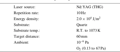
[image:1.595.307.547.679.784.2]The crystal phase was studied by thin film X-ray diffraction (XRD, Rigaku RAD-2C). The thickness was measured by a profilometer (Taylor-Hobson Talystep). X-ray photoelectron spectra (XPS, Surface Science SX100) were
Table 1 Deposition parameters.
Laser source: Nd:YAG (THG)
Repetition rate: 10 Hz
Energy density: 2:0104J/m2
Substrate: Quartz
Substrate temp.: R.T. to 1073 K
Target distance: 60 mm
Ambient: 106Pa
O2(0.13 to 67 Pa) *Graduate Student, Tohoku University
employed to investigate the binding energy of Ru, Sr and O atoms. The composition was studied by electron probe microanalysis (EPMA, JEPL JXA-8621MX). Surface mor-phology was observed by a field-emission scanning electron microscope (FESEM, JEOL JSM-6500FT). The electrical resistivity was measured in a temperature range between 60 and 298 K under a reduced He atmosphere, and between 298 and 673 K in air by the van der Pauw method.
3. Results and Discussion
Figure 1 shows XRD patterns of films prepared atPO2¼
13Pa andTsub ¼298to 973 K. Amorphous films with a halo
pattern were obtained at Tsub ¼298 and 573 K (Fig. 1(a)).
At Tsub>773K, peaks around 32 and 46 was identified,
which became significant with increasing Tsub. These peaks
could correspond to the (110) and (200) plane of pseudo-cubic SRO, respectively. At a high vacuum (P¼106) and
PO2¼0:13Pa, SRO thin films were amorphous with halo
patterns independent ofTsub.
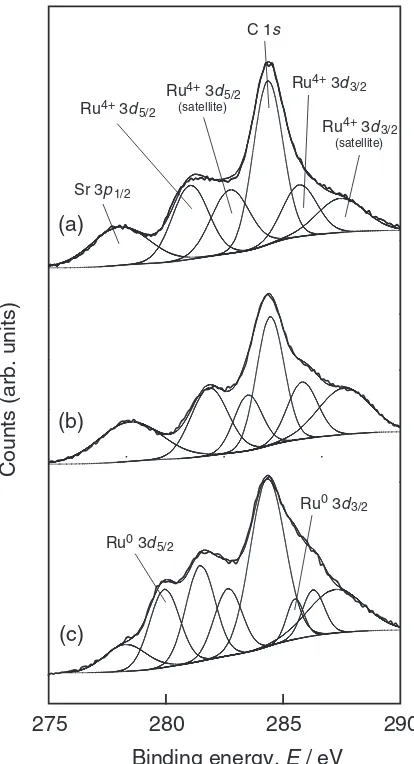
Figure 2 shows the Ru 3dXPS spectra of SRO thin films prepared at various conditions. The spectra were deconvo-luted by Gaussian functions with a baseline correction. The peak at 284.4 eV was assigned to carbon (C 1s) from contaminated hydrocarbon. At PO2¼13Pa and Tsub ¼973
K, the diffused peak was assigned to Sr 3p1=2 (278 eV), Ru 3d5=2 (281 and 283 eV) and Ru3d3=2 (286 and 288 eV) (Fig. 2(a)). It is known that the Ru3dspectrum has spin-orbit doublets at 281 and 286 eV with satellite peaks at 283 and
288 eV. The satellites are considered to result from the screening and unscreening of Ru3d cores by conduction electrons,13–15) although the highly oxidized Ru6þ state at surface might be associated with the satellite peaks.16,17) Figure 2(b) shows the Ru3dXPS spectra of SRO thin films prepared at PO2¼13Pa and Tsub¼298K. The binding
energies of Ru4þ 3dpeaks were 0.7 eV higher than those of Tsub ¼973K. The peaks at 280 and 285 eV of SRO thin films
prepared at PO2¼10
6Pa and T
sub¼973K could
corre-spond to Ru0 3d
5=2and Ru0 3d3=2, respectively, implying the co-deposition of metal Ru in the films (Fig. 2(c)). The Ru0 3d peaks were observed only in the SRO thin films prepared at P¼106Pa, in which the oxygen was insuffi-cient to obtain fully oxidized films.
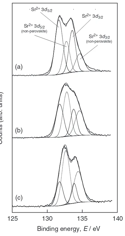
Figure 3 depicts the Sr3dXPS spectra of SRO thin films shown in Fig. 2. AtPO2¼13Pa andTsub ¼973K, two peaks
apparently corresponding to Sr3d5=2 and Sr3d3=2 (131 eV and 133 eV) were observed (Fig. 3(a)). The difference of 2 eV between the two Sr3d peaks was in good agreement with the reported value,18)whereas the ratio of Sr3d5=2peak to Sr3d3=2of the un-deconvoluted peak was contradicted by that of the spin-orbital interaction. AtTsub¼573and 298 K,
there was no splitting and one broadened peak was observed
2θ (Cu Kα) 20
(a) (b) (c)
25 30 35 40 45 50
Intensity (arb. units)
SrRuO3
(1
10)
(200)
Fig. 1 XRD patterns of SRO thin films prepared on quartz atPO2¼13Pa
andTsub¼298K (a), 773 K (b) and 973 K (c).
275 280 285 290
Binding energy, E / eV
Counts (arb. units)
Ru4+ 3d 5/2
Ru4+ 3d 5/2 (satellite)
Ru4+ 3d 3/2 (satellite) Ru4+ 3d
3/2
Ru0 3d 5/2
Ru0 3d 3/2 C 1s
Sr 3p1/2
(c) (b) (a)
[image:2.595.323.530.71.453.2] [image:2.595.73.268.72.384.2](Fig. 3(b)). AtP¼106Pa andT
sub¼973K, a doubly split
peak was obtained, but the Sr 3d peaks were almost 1 eV higher than those of PO2 ¼13Pa andTsub¼973K,
respec-tively. The Sr3d peaks of perovskite compounds such as SrRuO3,19,20) SrTiO321,22) and (Ba, Sr) TiO323) have been measured, and it has been reported that the binding energy of Sr in SrO (135 eV) is different from that in a perovskite structure.24)The abnormal ratio of Sr3d
5=2to Sr3d3=2would be caused by either a non-perovskite Sr-Ti-O cluster23)or
Sr-O segregation at the surface.21,22)By assuming
non-perov-skite Sr-O bonding with binding energy of 1 eV higher than the perovskite bonding, the Sr3d XPS spectra were deconvoluted into perovskite and non-perovskite peaks. The deconvoluted peaks of Sr3d5=2 (132 and 133 eV) and Sr 3d3=2 (134 and 135 eV) with the splitting energy (¼
2eV) are shown in Fig. 3, where the proportion of SSr3d5=2=SSr3d3=2¼3=2 was derived from the spin-orbital
interaction. The broad or apparently shifted Sr3d peaks can be well-deconvoluted with the perovskite and non-perovskite components. The non-perovskite component might increase with decreasingTsuband become significant at a high vacuum
ofP¼106Pa.
Figure 4 depicts the O1sXPS spectra of SRO thin films shown in Figs. 2 and 3. AtPO2¼13Pa andTsub ¼973K, an
O1speak at 528 eV and a broadened peak at around 530 eV were observed (Fig. 4(a)). The peak at 528 eV can be assigned to the perovskite structure of SRO.19,20) The broadened peak would originate from either the Ru4d eg
state,25) non-perovskite clusters19) or the state which is chemically different from the nonstoichiometry at the grain boundary or surface.20) It is difficult to specify the exact
reason for the broadened peak, and it is probably due to a combination of the above reasons. In this study, the O 1s peak was deconvoluted by perovskite and non-perovskite bondings. At PO2¼13Pa, the perovskite-bonding
compo-nent became smaller with decreasingTsub. A small peak at
535 eV was observed in Fig. 4(b). Since there is no SrO compound in the film, as shown in Fig. 3, this peak could be associated with Sr-O clusters or Sr-O termination at the surface.
Figure 5 shows the binding energy of the Ru3d5=2 peak for SRO thin films prepared atPO2 ¼13Pa andTsub ¼298to
973 K. With increasingTsub, the binding energy of the Ru4þ
peak increased from 281.1 to 281.8 eV.
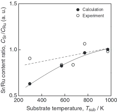
Figure 6 depicts the calculated and experimental Sr/Ru
125 130 135 140
Binding energy, E / eV
Counts (arb. units)
Sr2+ 3d 5/2
Sr2+ 3d 5/2 (non-perovskite)
Sr2+ 3d 3/2 (non-perovskite) Sr2+ 3d
3/2
(c) (b) (a)
Fig. 3 Sr3dXPS spectra of SRO thin films prepared atPO2¼13Pa and Tsub¼973K (a), 298 K (b), and atTsub¼973K andP¼106Pa (c).
Solid and dashed lines show perovskite and non-perovskite bonding, respectively.
525 530 535 540
Binding energy, E / eV
Counts (arb. units)
O2- 1s (non-perovskite)
O2- 1s (SrO) O2- 1s
(c) (b) (a)
[image:3.595.312.531.65.458.2] [image:3.595.69.278.69.462.2]content ratio (CSr=CRu) for SRO thin films prepared at PO2¼13Pa andTsub¼298to 973 K. The calculated values
were derived from the shift of the Ru4þ 3d5=2peak as shown in Fig. 5. Since the oxygen seems to be sufficiently supplied at PO2¼13Pa, the oxygen content may be assumed to be
almost constant in the SRO thin films. The shift of Ru 3dmay be associated with the valence number of Ru ions. By assuming that the valence of the Ru4þions slightly increases lineally toward Ru6þto compensate for the Sr deficiency, the Sr/Ru content ratio can be calculated by eq. (1).
CSr=CRu¼ ðBERuVIBERuMeasuredÞ=ðBERuVIBERuIVÞ;
ð1Þ
where BERu is the binding energy of Ru3d, BERuIV¼
281eV andBERuVI¼283eV.26)The trend of the calculated CSr=CRu values was similar to that of the experimental
values, and decreased with decreasing Tsub. Although the
experimental values were slightly smaller than those of the calculated values, the trends of the two coincided well. Sr
atoms in the non-perovskite Sr-O structure were more numerous in the thin films prepared at lower Tsub, thus
leading to formation of an Sr deficient perovskite structure which caused the shift of Ru4þ 3dpeak.
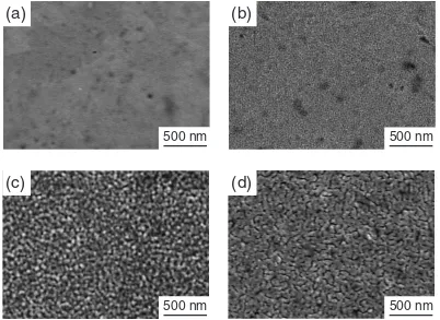
Figure 7 shows the surface morphology of SRO thin films prepared atPO2¼13Pa andTsub¼298to 973 K. A
hetero-geneous texture with droplets and pores was observed at Tsub ¼298K (Fig. 7(a)), and a uniform fine grained texture
was obtained at Tsub ¼773K (Fig. 7(b)). The grain size
increased from 20 nm atTsub ¼973K (Fig. 7(c)) to 100 nm
[image:4.595.69.267.72.249.2]with an island-like texture atTsub¼1073K (Fig. 7(d)).
Figure 8 shows the surface morphology of SRO thin films prepared at Tsub¼973K and various atmospheres. A
porous, non-uniform surface was observed at P¼106Pa (Fig. 8(a)). Small grains of several nm in size with a porous texture were observed at PO2¼0:13Pa (Fig. 8(b)).
Well-crystallized grains with uniform texture were obtained at PO2¼13Pa (Fig. 8(c)). The grain size increased to more
than 50 nm and formed a network texture at PO2 ¼67Pa
(Fig. 8(d)).
As shown in Figs. 7 and 8, well-crystallized SRO thin films were not obtained at lowPO2andTsub, and the grain size
became coarse and rough at higher Tsub and PO2. The
appropriate condition to prepare SRO thin film with a homogeneous, fine-grained texture was PO2¼13Pa and
Tsub ¼973K.
Figure 9 shows the temperature dependence of the electrical resistivity from room temperature to 673 K for SRO thin films prepared at various conditions. For SRO thin films prepared at PO2¼13Pa, the electrical resistivity at
room temperature decreased from 9:9104 to 8:8
106m with increasing T
sub (Figs. 9(a)–(d)), and at Tsub >773K the films exhibited metallic conduction.
Al-though SRO thin films prepared at Tsub¼973K and P¼106Pa exhibited a high resistivity of2:0103m with semi-conductor-like conduction behavior (Fig. 9(e)), the films prepared at PO2¼0:13Pa and 65 Pa at Tsub¼
973K were 1:7105m and 1:5105m with me-tallic conduction, respectively (Figs. 9(f) and 9(h)). These results suggest that the Tsub rather than PO2 significantly
affected the electrical resistivity of SRO thin film. This tendency could correspond to those obtained by XRD and XPS, in which the effect of PO2 on the composition and
chemical bonding was also less influenced by that ofTsub.
Figure 10 shows the temperature dependence of the electrical resistivity from 60 K to room temperature for SRO thin films prepared at PO2¼13Pa and Tsub¼573 to
973 K. SRO thin films prepared at Tsub ¼573K exhibited
semi-conductor-like behavior (Fig. 10(a)), but those at Tsub >673K showed metallic conduction (Figs. 10(b)–(d)).
The temperature gradient of electrical resistivity changed at T ¼163K (Fig. 10(d)), which coincided with the Curie temperature (TC), indicating a magnetic phase transition. The
change of temperature gradient belowTCcould be explained
by the effect of the decreasing spin scattering on the electrical resistivity in the ferromagnetic phase.27)On the other hand, no change atTCwas observed for SRO thin films prepared at Tsub <773K. It is known that there is a strong correlation
between the magnetic/electric properties and the crystal structure,i.e., Ru-O-Ru distance and the connection angle of 282.0
281.5
281.0
280.5
200 400 600 800 1000
Substrate temperature, Tsub / K
Peak position of Ru 3
d5/2
,
E
/ eV
Fig. 5 Effect of substrate temperature on XPS peak position of Ru3d5=2
for SRO thin films prepared at PO2¼13Pa and various substrate
temperatures.
Experiment Calculation
200 400 600 800 1000
1.5
1.0
0.5
Substrate temperature, Tsub / K
Sr/Ru content ratio,
CSr
/
CRu
(a. u.)
[image:4.595.70.267.313.502.2]the RuO6 octahedral.6,28) Since the structure of SRO thin films prepared at low Tsub might be slightly more distorted
than those prepared at higherTsub, the change of temperature
gradient of electrical resistivity at the TC was not evident.
Therefore, the temperature dependence of electrical con-ductivity around TC can be a good indication of the
(c)
(d)
(a)
(b)
1
µ
m
1
µ
m
1
µ
m
1
µ
m
Fig. 7 SEM images of surface morphology of SRO thin films prepared atPO2¼13Pa andTsub¼298K (a), 773 K (b), 973 K (c)
and 1073 K (d).
(c)
(d)
(a)
(b)
500 nm
500 nm
500 nm
500 nm
Fig. 8 SEM images of surface morphology of SRO thin films prepared atTsub¼973K andP¼106(a) andPO2¼0:13Pa (b), 13 Pa (c)
[image:5.595.100.498.72.368.2] [image:5.595.97.499.408.701.2]crystallinity of SRO films. SRO in the form of a single-crystal and epitaxially grown film have been well studied and theTC
has been identified. However, no study on polycrystalline SRO thin films prepared on quartz substrates has been reported. Although the SRO thin films prepared in this study were poly-crystalline, they indicated theTC, suggesting high
quality, well-crystallized SRO thin films.
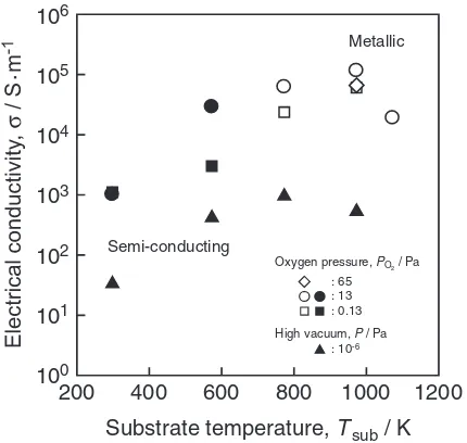
Figure 11 summarizes the effects of Tsub andPO2 on the
electrical conductivity of SRO thin films. Highly conductive SRO thin films were obtained at higher Tsub andPO2. The
SRO thin films having high crystallinity without Sr defi-ciency prepared at higher Tsub and PO2 would be highly
conductive with metallic conduction. The electrical conduc-tivity slightly decreased at higherTsubandPO2. That would be
caused by surface morphology due to island growth (Fig. 7(d)) and the coarse-grained surface (Fig. 8(d)). As shown in Fig. 9, the highly conductive SRO thin film exhibited metallic conduction whereas the less conductive SRO thin film trended to be semi-conducting.
4. Conclusions
SRO thin films were prepared by laser ablation on quartz substrates. SRO thin films were amorphous atP¼106and PO2¼0:13Pa. AtPO2¼13Pa andTsub>773K, SRO thin
films were well crystallized into a pseudo-cubic perovskite structure. Non-perovskite Sr-O clusters with slight Sr deficiency of the perovskite structure were possibly con-tained in the SRO thin films prepared at low Tsub, and
metallic Ru was identified atP¼106Pa. Well-crystallized fine grains were obtained at PO2¼13Pa andTsub ¼973K.
The electrical resistivity of SRO thin films prepared at PO2¼13Pa decreased from 9:910
4 to8:8106m
200 300 400 500 600 700
10-2
10-3
10-4
10-5
10-6
h f e
g 10-3
10-4
10-5
10-6
d c b a
Temperature, T / K
Fig. 9 Temperature dependence of electrical resistivity of SRO thin films prepared atPO2¼13Pa andTsub¼293K (a), 573 K (b), 773 K (c) and
973 K (d), and atTsub¼973K andP¼106Pa (e), andPO2¼0:13Pa (f),
13 Pa (g) and 67 Pa (h).
50 100 150 200 250 300
10-4
10-5
10-3
10-1
10-2
d c
b a
[image:6.595.72.269.72.413.2]Temperature, T / K TC
Fig. 10 Temperature dependence of electrical resistivity at low temper-atures for SRO thin films prepared atPO2¼13Pa andTsub¼573K (a),
673 K (b), 773 K (c) and 973 K (d). The vertical scale for plot (a) is modified.
200 400 600 800 1000 1200 106
105
104
100
101
102 103
Substrate temperature, Tsub / K
Metallic
Semi-conducting
: 65 : 13 : 0.13
: 10-6 Oxygen pressure, PO2 / Pa
High vacuum, P / Pa
[image:6.595.326.524.73.350.2] [image:6.595.320.535.421.625.2]with increasingTsubassociated with Sr deficient composition.
A further increase in Tsub and PO2 caused a decrease in
electrical conductivity due to the coarse grain surface morphology. High crystallinity polycrystalline SRO thin films showed a change of electrical resistivity at a TC of
160 K, related to the magnetic phase transition.
Acknowledgements
This research was supported in part by a COE program at Institute for Materials Research, Tohoku University. We are grateful to N. Ohtsu and Y. Murakami at the Advanced Research Center of Metallic Glasses, Institute for Materials Research for XPS measurement and EPMA analysis, re-spectively. This research was financially supported in part by Furuya Metal Co., Ltd. and Lonmin Plc.
REFERENCES
1) P. B. Allen, H. Berger, O. Chauvet, L. Forro, T. Jarlborg, A. Junod, B. Revaz and G. Santi: Phys. Rev. B53(1996) 4393–4398.
2) C. B. Eom, R. B. Van Dover, J. M. Phillips, D. J. Werder, J. H. Marshall, C. H. Chen, R. J. Cavaand, R. M. Flemingand and D. K. Fork: Appl. Phys. Lett.63(1993) 2570–2572.
3) T. Morimoto, O. Hidaka, K. Yamakawa, O. Arisumi, H. Kanaya, T. Iwamoto, Y. Kumura, I. Kunishima and S. Tanaka: Jpn. J. Appl. Phys. 39(2000) 2110–2213.
4) O. Kuffer and Ø. Fischer: J. Appl. Phys.97(2005) 014103. 5) R. Ohara, T. Schimizu, K. Sano, M. Yoshiki and T. Kawakubo: Jpn. J.
Appl. Phys.40(2001) 1384–1387.
6) Z. Sefrioui, D. Arias, M. A. Navacerrada, M. Varela, G. Loos, M. Lucı´a, J. Santamarı´a, F. S. -Quesadaand and M. A. Lo´pez de la Torre: Appl. Phys. Lett.73(1998) 3375–3377.
7) K. Takahashi, T. Oikawa, K. Saito, S. Kaneko, H. Fujisawa, M. Shimizu and H. Funakubo: Jpn. J. Appl. Phys.41(2002) 5376–5386.
8) H. Funakubo, T. Oikawa, N. Higashi and K. Saito: J. Crystal Growth 235(2002) 401–406.
9) M. Hiratani, C. Okazaki, K. Imagawa and K. Takagi: Jpn. J. Phys.35 (1996) 6212–6216.
10) K. Watanabe, M. Ami and M. Tanaka: Mater. Res. Bull.32(1997) 83– 96.
11) X. Fangand and T. Kobayashi: J. Appl. Phys.90(2001) 162–166. 12) X. D. Wu, S. R. Foltyn, R. C. Dye, Y. Coulter and R. E. Muenchausen:
Appl. Phys. Lett.62(1993) 2434–2436.
13) P. A. Cox, J. B. Goodenough, P. J. Tavener, D. Telles and R. G. Egdell: J. Solid State Chem.62(1986) 360–370.
14) Y. J. Kim, Y. Gao and S. A. Chambers: Appl. Surf. Sci.120(1997) 250–260.
15) H. Over, A. P. Seitsonen, E. Lundgren, M. Smedh and J. N. Andersen: Surf. Sci.504(2002) L196–L200.
16) H. J. Lewerenz, S. Stucki and R. Ko¨tz: Surf. Sci.126(1983) 463–468. 17) P. Froment, M. J. Genet and M. Devillers: J. Electron. Spectrosc. Relat.
Phenom.104(1999) 119–126.
18) J. C. Fuggle and N. Ma˚rtensson: J. Electron Spectrosc. Relat. Phys.21 (1980) 275–281.
19) J. Shin, S. V. Kalinin, H. N. Lee, H. M. Christen, R. G. Moore, E. W. Plummerand and A. P. Baddorf: Surf. Sci.581(2005) 118–132. 20) J. Kim, J. Chungand and S.-J. Oh: Phys. Rev. B71(2005) 121406. 21) K. Szot, W. Speier, U. Breuer, R. Meyer, J. Szadeand and R. Waser:
Surf. Sci.460(2000) 112–128.
22) P. A. W. van der Heide, Q. D. Jiang, Y. S. Kimand and J. W. Rabalais: Surf. Sci.473(2001) 59–70.
23) J. X. Liao, C. R. Yang, J. H. Zhang, C. L. Fu, H. W. Chenand and W. J. Leng: Appl. Surf. Sci. (in press).
24) H. van Doverenand and J. A. TH. Verhoeven: J. Electron Spectrosc. Relat. Phenom.21(1980) 265–273.
25) J. Park, S.-J. Oh, J.-H. Park, D. M. Kimand and C.-B. Eom: Phys. Rev. B69(2004) 085108.
26) S. Bhaskar, P. S. Dobal, S. B. Majumderand and R. S. Katiyar: J. Appl. Phys.89(2001) 2987–2992.
27) L. Klein, Y. Kats, N. Wiser, M. Konczykowski, J. W. Reiner, T. H. Geballe, M. R. Beasleyand and A. Kapitulnik: Europhys. Lett. 55 (2001) 532–538.