Bondability of Copper Joints Formed Using a Mixed Paste
of Ag
2O and CuO for Low-Temperature Sinter Bonding
Tomo Ogura
+, Tomohiro Yagishita, Shinya Takata, Tomoyuki Fujimoto and Akio Hirose
Division of Materials and Manufacturing Science, Graduate School of Engineering, Osaka University, Suita 565-0871, JapanThe bondability of copper joints formed using a mixed paste of silver oxide (Ag2O) and copper oxide (CuO) that contained reducing solvents was evaluated in order to achieve bonds that exhibited high migration tolerance and could serve as Pb-free alternatives to the conventional bonds formed using high-melting point solders in electronics packaging. The Ag2O particles reduced into silver nanoparticles at 150°C, whereas the CuO reduced into copper nanoparticles about 300°C. The joints formed using the Ag2O/CuO mixed paste, when heated to the appropriate levels, exhibited bondability superior to that of conventional Pb5Sn joints. The oxidefilm formed on the copper substrate was reduced by the combustion of polyethylene glycol 400, and bonding was achieved between the sintered layer and the copper substrate. A longer period resulted in the oxidisation of a few layers of sintered copper layers into Cu2O. The ion-migration tolerance of the Ag2O/CuO mixed paste was approximately four times that of a layer of pure sintered silver. [doi:10.2320/matertrans.MD201202]
(Received November 30, 2012; Accepted February 18, 2013; Published April 5, 2013)
Keywords: silver oxide, copper oxide, ion migration, sintering, nanoparticles, copper joint
1. Introduction
It is desirable that electronic devices not only work efficiently at elevated temperatures but also consume lesser power when packaged. However, bonding technology that can meet these requirements needs to be developed. In particular, there is a pressing demand for suitable alternatives to lead-rich high-melting-point solders, which contain chemi-cal substances that are hazardous to the environment. The difficulty in developing lead-free solders for use at high temperatures arises from the requirement that the metallic bonds between mounted parts of semiconductor chips and various wiring connections exhibit long-term reliability. The mounted components of semiconductor chips (i.e., die-bonded parts) generate considerable heat and thus need improved thermal resistance. In addition, the discharge characteristics of certain parts of semiconductor chips must be maintained to enable the stable operation of the chips.1,2) It is anticipated that the use of nanoparticles as bonding materials in die-attach technologies will provide feasible alternatives to the current microsoldering techniques that require the use of high-temperature solders such as Pb10Sn or Pb5Sn. This is because particles smaller than 10 nm in size exhibit characteristics significantly different from those of the bulk state.36)This phenomenon is owing to the large
surface energy of the nanoparticles. If activated nanoparticles could be made to affect the surface atoms of the bulk metal being bonded, metal-to-metal bonding using the nano-particles asfiller material could be achieved at significantly lower temperatures than those in the case of conventional fusion welding or diffusion bonding. This unique property of nanoparticles could be exploited in bonding materials in electronic devices in order to achieve the improved thermal characteristics discussed above.
The use of nanoparticles as bonding materials for die-attach technologies is attracting significant research interest, and there have been numerous studies exploring nanoparticle pastes for use in low-temperature sintering.711)Researchers
have proposed a novel bonding process that involves silver nanoparticles.2,1215) In addition, silver nanoparticles have been formed in-situ from silver oxide particles,1,1620) and these silver nanoparticles are being explored as an alternative to the high-temperature solders currently used, such as Pb 10Sn or Pb5Sn. Researchers have also studied the dynamics of the initial stage of the sintering of nanoparticles on metal substrates using molecular dynamics (MD) simulation studies.21)When bonding techniques involving the sintering
of nanoparticles are used in the assembly of fine pitch electronic devices, attention must be paid to the ion-migration tolerance of the bonded circuits, since a sintered layer of pure Ag is formed on them.22) It has been found that the
ion-migration tolerances of the sintered layers improve with the addition of gold and palladium particles in the form of a second metal to the Ag2O paste.19)However, these metals are
expensive, resulting in an increase in costs, whereas, from an industrial point of view, it is important to devise sintering methods that are cheaper.
In this study, CuO was chosen as an alternative to gold and palladium and used so as to add a second metal to the Ag2O
paste. This was done in the hope that CuO would be reduced by the solvent during bonding, and the formed copper nanoparticles would get distributed in the sintered silver, preventing the migration of the silver atoms. Yanet al.also reported the addition of cupper to silver improves bondability of joints using CuAg mixed nanoparticles.23) The
bond-ability of the joints formed using a reducing-solvents-containing mixed paste of silver oxide (Ag2O) and copper
oxide (CuO) was investigated.
2. Experimental Procedure
Ag2O particles and CuO particles were prepared as shown
in Fig. 1. The Ag2O particles and CuO particles were mixed
in the ratio of 9 : 1 (in mass%) in the combined solvents of polyethylene glycol (PEG) 400 and a viscous solvent, used in a concentration of 180 µl/g, and processed into a paste for bonding. A copper substrate was used as the material to be bonded. The paste was applied to a lower sample that was
+Corresponding author, E-mail: tomo.ogura@mapse.eng.osaka-u.ac.jp Special Issue on Nanojoining and Microjoining
10 mm in diameter and 25 mm in length and then preheated to 80°C. Next, an upper sample measuring 5 mm in diameter and 15 mm in length was placed on top of the lower sample and bonded at temperatures ranging from 300 to 400°C. The bonding was carried out in an infrared furnace for 5 min under pressure of 5 MPa, applied using a dead weight mounted on top of the upper sample. The joint strength of the formed bond was evaluated using a tensile test performed at a cross-head speed of 1 mm/min. The thermal characteristics of the combined paste were determined using a combination of thermogravimetric (TG) and differential thermal (DT) analy-ses, performed using a heating rate of 10°C/min in ambient atmosphere. The cross section of the joint was observed using transmission electron microscopy (TEM). The ion-migration tolerance of the sintered layer was evaluated using the previously employed water drop method.19) The bonding
pastes were applied to a glass substrate. Then, the pastes sintered at 300°C for 300 s under pressure after preheated. A 10 µl droplet of distilled water was placed on the gap between the sintered samples, and a voltage of 3 V was applied across the samples. On the application of the voltage, silver ions migrated from the anode to the cathode, and silver dendrites grew in the direction of the anode. The time taken by the silver dendrites to reach the anode was measured.
3. Results and Discussion
3.1 Reduction behaviour of the Ag2O/CuO mixed paste
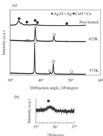
Figure 2 shows TG-DT analyses curves of the mixed paste of Ag2O/CuO. Two exothermal peaks, at 150°C and at
300°C, were observed. A corresponding loss in the weight of the paste sample was also confirmed. Figure 3 shows the X-ray diffraction (XRD) patterns of the Ag2O/CuO mixed
paste samples that had been heated to 150 and 300°C. The XRD pattern of the paste sample heated to 150°C showed peaks attributable to silver and CuO, whereas the XRD pattern of the paste sample heated to 300°C showed peaks attributable to silver and copper. On the basis of the TG-DT analyses curves and the XRD patterns of the paste samples, it was determined that Ag2O particles reduced into silver
nanoparticles at 150°C. In addition, CuO also reduced into copper nanoparticles at about 300°C. Residual amounts of the PEG solvent remained in the bonding layer until the bonding temperature reached 150°C, at which point the redox reaction reached completion.20) Therefore, the reduction of
CuO was considered to be proceeded by the residual PEG solvent because PEG solvent did not evaporate and combust until the temperature reached 300°C.20)
1
μ
m
1
μ
m
(a) (b)
Fig. 1 SEM images of (a) Ag2O and (b) CuO particles.
-25 -20 -15 -10 -5 0
-200 0 200 400 600 800 1000
0 100 200 300 400
DTA TG
DT
A (
μ
V)
TG (mass%)
Temperature, T /°C
Fig. 2 TG-DTA curves of the Ag2O/CuO mixed paste.
Non heated
423K Ag2O Ag CuO Cu
573K
(a)
(b)
Intensity (a.u.)
40°
Diffraction angle, 2θ/degree
30° 50° 60°
Intensity (a.u.)
2θ/degree 37° 36°
35°
[image:2.595.114.485.69.192.2] [image:2.595.322.527.231.502.2] [image:2.595.76.262.234.389.2]3.2 Tensile strength of the joints
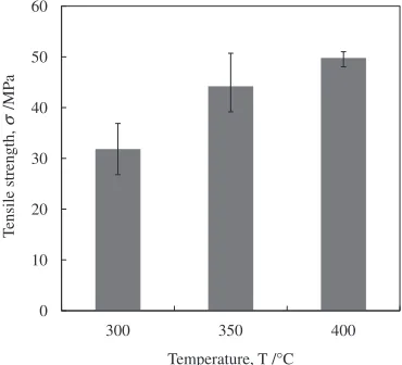
Figure 4(a) shows tensile strength of the joints formed using the Ag2O/CuO mixed paste heated to 400°C. The
strength of the joints could be measured at 250°C. At 300°C, the strength increased, owing to the formation and sintering of copper nanoparticles and the evaporation and combustion of the residual PEG solvent. In general, the strength increased with increases in the temperature and the holding time (see Fig. 4(b)). Figure 5 shows the tensile strengths of joints heated to various temperatures and held at those temperatures for 300 s. Again, the strength increased with an increase in the bonding temperature, and all specimens exhibited has higher strengths than those of gold-to-gold joints formed using Pb5Sn (29 MPa), which is the current industrial standard for die bonding. This showed clearly that when the
joints formed using the Ag2O/CuO mixed paste were heated
to appropriately high temperatures, the bonding achieved was superior to that obtained using Pb5Sn.
The fractured surface of a joint after the tensile test is shown in Fig. 6. It was confirmed that some silver particles sintered with the copper substrate at 200°C (Fig. 6(a)). The number of sintered particles present on the fractured surface increased as with temperature (Figs. 6(b) and 6(c)). The
Holding time, t /s 0
10 20 30 40 50 60
0 60 120 180 240 300
(a)
(b) 0 10 20 30 40 50 60
100 150 200 250 300 350 400 Temperature, T /°C
T
ensile strength,
σ
/MP
a
T
ensile strength,
σ
/MP
a
Fig. 4 Tensile strengths of the joints formed using the Ag2O/CuO mixed paste (a) heated till up to 400°C and (b) held at 400°C for various periods, with the bonding pressure being 5 MPa.
0 10 20 30 40 50 60
300 350 400
Temperature, T /°C
T
ensile strength,
σ
/MP
a
Fig. 5 Tensile strengths of the joints formed using the Ag2O/CuO mixed paste and heated to various temperatures, while being held at the temperatures for 300 s. The bonding pressure used was 5 MPa.
1mm
5
μ
m
1mm
5
μ
m
1mm
5
μ
m
1mm
5
μ
m
(a)
(b)
(c)
(d)
[image:3.595.306.548.60.615.2] [image:3.595.77.263.68.306.2] [image:3.595.77.262.376.544.2]dimple-like fracture region also increased in area (Figs. 6(c) and 6(d)), indicating that the sintering of not only silver nanoparticles but also of copper nanoparticles occurred after the reduction of CuO. In addition, with an increase in the holding time, the circumferential regions of the fractured surfaces of the joints were increasingly seen to contain a black region, which is typically observed on the surface of copper oxide,20) showing that the oxidation of both the copper substrate and sintered copper nanoparticles started during the heating process.
3.3 Microstructures of the interfaces of the joints
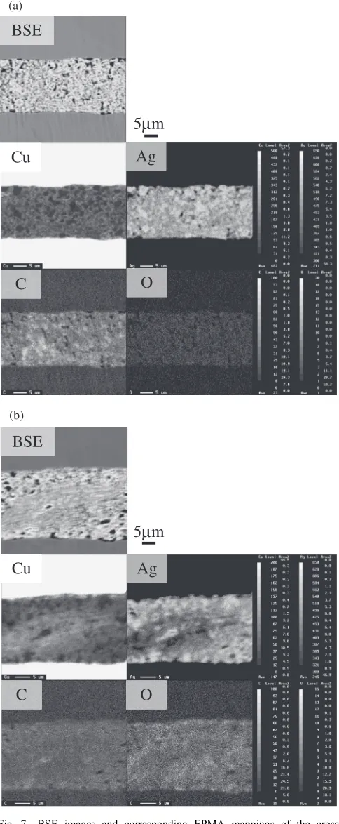
Figure 7 shows the back-scattered electron (BSE) images and the corresponding results of electron probe micro-analyzer (EPMA)-based element mapping of the cross sections of the joints bonded using the Ag2O/CuO mixed
paste. While gold and palladium are concentrated in distinct phases in the sintered silver layer in joints formed using a gold- and palladium-supplemented Ag2O paste,19) it was
found that copper was uniformly distributed in the sintered silver layer in the joints formed using the Ag2O/CuO mixed
paste (Fig. 7(a)). Holding the joint for 300 s increased the concentration of oxygen around copper, as shown in Fig. 7(b). This increase in the oxygen concentration was probably owing to the formation of copper oxide. A layer of copper oxide was distinctly observable using TEM. Figure 8 shows brightfield and energy-dispersive X-ray spectroscopy (EDS) mapping images of the joint formed using the Ag2O/
CuO mixed paste and heated to and held at 400°C for 300 s. A film of the natural oxide of copper was not observed, showing the bond formed was achieved between the sintered layer and the copper substrate. The oxidefilm on the copper substrate was reduced by the combustion of PEG, and the residual PEG suppressed the oxidation of the copper substrate during bonding.20)The results of the EDS mapping confirmed the presence of silver and of a copper layer, with the oxygen being present within the copper layer. A magnified image of the sintered layer along with the corresponding SAED pattern and the results of the EDS analysis of the layer are shown in Fig. 9 and Table 1. The SAED patterns indicated the presence of silver, copper and Cu2O. However, CuO was not detected. The formation of
Cu2O was probably owing to the oxidation of a few layers of
sintered copper during the heating process.24)The results of
the EDS analysis also suggested that a few sintered layers were in the form of a solid solution of the silver and copper nanoparticles (point 1 in Table 1), indicating that some of the copper nanoparticles were alloyed with the silver during the formation and sintering of the copper nanoparticles.
3.4 Ion-migration tolerance
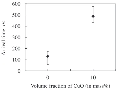
In the water-drop test, Ag atoms of the anode were ionised and made to pass through water towards the cathode under an electricfield. On reaching the cathode, these Ag precipitated, forming Ag dendrites. The Ag dendrites grew in size and eventually reached the anode. The “arrival time” for the dendrites, which was defined as from the time period extending from the application of the 3 V potential to the moment the Ag dendrites reached the anode, was used as a measure of the ion-migration tolerance. Figure 10 shows the
arrival time plotted against the volume fraction of CuO in the sintered layer. The arrival time for the mixed paste was approximately four times as large as that of a layer of pure sintered silver. Although the quantitative evaluation such as migration rate is not clarified yet, thus, the addition of CuO improved the ion-migration tolerance of the sintered silver layer. There are several possible reasons this improvement in
Cu
C
Ag
O
BSE
Cu
C
Ag
O
BSE
5
μ
m
(a)
(b)
5
μ
m
[image:4.595.307.549.72.659.2]the ion-migration tolerance. The addition of a second metal reduces the area fraction of silver on the surface of the anode. This reduction can result in a reduction in the amount of ionised silver atoms at the anode because copper migrates to a lesser degree than silver. During the migration of silver atoms, the concentration of the second metal increases at the anode surface, preventing the further migration of silver atoms from the anode.19) Moreover, the diffusion of Ag
atoms through the sintered Ag layer may be disrupted owing to the presence of the sintered layer of the second metal. This disruption may be an additional mechanism owing to which the second metal prevents the migration of silver atoms. The limiting additive fraction of CuO is not revealed yet and the further research is needed for better understanding of this point.
4. Conclusions
(1) Ag2O particles reduced into silver nanoparticles at
150°C. Then, CuO reduced into copper nanoparticles at about 300°C. The reduction of CuO was considered to be attributable to the presence of the residual PEG solvent.
(2) The joints formed using the Ag2O/CuO mixed paste,
when heated to the appropriate levels, exhibited bond-ability superior to that of a conventional Pb5Sn joint.
(3) Bonding was achieved between the sintered layer and the copper substrate. The oxide film on the copper substrate was reduced by the combustion of PEG. A longer heating period resulted in the oxidisation of a
B.F. Ag
Cu O
500nm Interface
Fig. 8 Brightfield and EDS mapping images of the joint formed using the Ag2O/CuO paste. The joint was heated to 400°C and held at this temperature for 300 s with a bonding pressure of 5 MPa.
1
2
100nm
Cu substrate
(a)
Interface
Cu{220}
Ag{220} Cu2O{220}
(b)
Cu{111}
Fig. 9 (a) Brightfield image of a joint and (b) diffraction pattern of the encircled region of the joint.
0 100 200 300 400 500 600
0 10
Arri
v
al time,
t
/s
[image:5.595.48.290.68.308.2]Volume fraction of CuO (in mass%)
[image:5.595.313.539.68.492.2]Fig. 10 Time taken by the silver dendrites in the sintered layer to grow from the anode and reach the cathode during the water-drop test. This parameter was termed the“arrival time”of the dendrites.
Table 1 Results of a quantitative EDS analysis of the area of the joint shown in the TEM image in Fig. 9(a).
Composition (%)
Ag Cu O
1 25.6 65.4 9.0
[image:5.595.46.292.393.449.2] [image:5.595.334.519.535.676.2]few layers of sintered copper into Cu2O. A few of the
sintered layers acted as a solid solution of the silver nanoparticles and the copper nanoparticles.
(4) The ion-migration arrival time of the Ag2O/CuO mixed
paste was approximately four times that of pure sintered silver.
Acknowledgements
The authors would like to thank Prof. M. Takahashi of Osaka University and Prof. T. Shibayanagi of Osaka University (now at Toyama University) for their valuable help with the TEM observations, and thank Mr. K. Ohmitsu for his help with the EPMA operations. A part of this study was performed under the Cooperative Research Program of Institute for Joining and Welding Research Institute, Osaka University. This work was supported by a Grant-in-Aid for Scientific Research (B) No. 23360322, Japan, and by Priority Assistance for the Formation of Worldwide Renowned Centers of Research®The Global COE Program (Project: Center of Excellence for Advanced Structural and Functional Materials Design) from the Ministry of Education, Culture, Sports, Science and Technology (MEXT), Japan.
REFERENCES
1) T. Morita, Y. Yasuda, E. Ide, Y. Akada and A. Hirose:Mater. Trans.49 (2008) 28752880.
2) T. Morita, E. Ide, Y. Yasuda, A. Hirose and K. F. Kobayashi:Jpn. J. Appl. Phys.47(2008) 66156622.
3) A. N. Goldstein, C. M. Echer and A. P. Alivisatos:Science256(1992) 14251427.
4) P. Pawlow: Z. Phys. Chem.65(1909) 545548. 5) M. Takagi:J. Phys. Soc. Japan9(1954) 359363.
6) N. Gladkich, R. Niedermayer and K. Spiegel:Phys. Status Solidi15 (1966) 181192.
7) J. G. Bai and G. Q. Lu:IEEE Trans. Device Mater. Reliab.6(2006) 436441.
8) A. Hu, J. Y. Guo, H. Alarifi, G. Patane, Y. Zhou, G. Compagnini and C. X. Xu:Appl. Phys. Lett.97(2010) 153117.
9) Y. Morisada, T. Nagaoka, M. Fukusumi, Y. Kashiwagi, M. Yamamoto, M. Nakamoto, H. Kakiuchi and Y. Yoshida:J. Electron. Mater. 40 (2011) 23982402.
10) K. Suganuma, S. Sakamoto, N. Kagami, D. Wakuda, K. S. Kim and M. Nogi:Microelectron. Reliab.52(2012) 375380.
11) Y. Kobayashi, T. Shirochi, Y. Yasuda and T. Morita:Int. J. Adhes. Adhes.33(2012) 5055.
12) Y. Akada, H. Tatsumi, T. Yamaguchi, A. Hirose, T. Morita and E. Ide: Mater. Trans.49(2008) 15371545.
13) E. Ide, S. Angata, A. Hirose and K. F. Kobayashi:Acta Mater. 53 (2005) 23852393.
14) E. Ide, A. Hirose and K. F. Kobayashi:Mater. Trans.47(2006) 211 217.
15) Y. Zhou (ed.):Microjoining and nanojoining, (Woodhead Publishing Limited, Cambridge, 2008) pp. 250268.
16) A. Hirose, H. Tatsumi, N. Takeda, Y. Akada, T. Ogura, E. Ide and T. Morita:J. Phys. Conf. Ser.165(2009) 012074.
17) T. Morita, Y. Yasuda, E. Ide and A. Hirose:Mater. Trans.50(2009) 226228.
18) A. Hirose, N. Takeda, Y. Konaka, H. Tatsumi, Y. Akada, T. Ogura, E. Ide and T. Morita:Mater. Sci. Forum706709(2012) 29622967. 19) T. Ito, T. Ogura and A. Hirose:J. Electron. Mater.41(2012) 2573
2579.
20) S. Takata, T. Ogura and A. Hirose:J. Electron. Mater.42(2013) 507 515.
21) T. Ogura, M. Nishimura, H. Tatsumi, W. Takahara and A. Hirose: Mater. Trans.53(2012) 20852090.
22) E. Ide, T. Morita and Y. Kawachi: Proc. 24th JIEP Ann. Meeting, (2010) pp. 210211.
23) J. Yan, G. Zou, A. Wu, J. Ren, A. Hu and N. Zhou:J. Electron. Mater. 41(2012) 18861892.