ELECTRON BEAM LITHOGRAPHY AND INDUCED DEPOSITION
FOR NANOPLASMONIC APPLICATIONS
Aline Heyerick
A Thesis Submitted for the Degree of MPhil
at the
University of St Andrews
2018
Full metadata for this item is available in
St Andrews Research Repository
at:
http://research-repository.st-andrews.ac.uk/
Please use this identifier to cite or link to this item:
http://hdl.handle.net/10023/12891
Electron Beam Lithography and Induced Deposition
for Nanoplasmonic Applications
Aline Heyerick
This thesis is submitted in partial fulfilment for the degree of MPhil
at the
University of St Andrews
Abstract
Nanoplasmonics concerns the study of light-metal interactions on a subwavelength scale, exhibiting behaviour able to achieve arbitrary control and manipulation of light at the nanoscale, an important goal for the further development of nanophotonic devices. As the field of plasmonics advances,
re-search is looking beyond the materials and fabrication techniques traditionally employed. This thesis discusses the design, fabrication methods, and characterisation of nanoplasmonic structures. A
com-parison between two electron beam based fabrication techniques, electron beam lithography (EBL) and electron beam induced deposition (EBID), is presented. The discussion covers both the fabri-cation technology and the properties of the resulting nanoscale structures: gold nanoscale features
obtained via standard EBL, and tungsten structures achieved through EBID. As a mature technology, the well-understood characteristics and reliable fabrication procedures of electron beam lithography
are weighed up against the limitations of top-down planar fabrication. Electron beam induced depo-sition is presented as an alternative technology, able to achieve nanoscale fabrication resolution with
a point-and-shoot bottom-up deposition technique, but constrained by the lack of optimised fabri-cation settings as a result of incomplete understanding of a complex set of patterning parameters. Direct-write EBID technology offers to overcome several of the limitations and challenges of electron
beam technology, including three-dimensional and greyscale patterning, and precise alignment and orientation of nanoscale features on arbitrary substrate patterns.
This thesis also presents the discussion of chirped plasmonic diffraction gratings as a specific appli-cation in nanoplasmonics. Their theoretical design based on Fourier analysis and simulation-based design, their fabrication using both electron beam lithography and induced deposition, as well as the
characterisation of their far-field diffraction pattern are discussed in detail. As part of the character-isation step, a Fourier microscopy setup for the measurement of the far-field diffraction patterns of
Acknowledgements
During the course of this research I received help from many people. First and foremost I need to thank Dr Andrea Di Falco, my supervisor, who was a guide throughout the project. Special thanks should be given to Blair Kirkpatrick, Peter Reader-Harris, and Monika Pietrzyk, who offered valuable
advice and taught me how to use various pieces of fabrication equipment, an essential skill. I am very grateful for the assistance I received from Dr Liam O’Faolain, as my second supervisor, and for
the help and advice I received from Professor Manfred Buck and Dr Renald Shaub of the School of Chemistry, who were there to help with the parts of the research requiring a lot of chemical knowledge. I also want to thank the other members of the Synthetic Optics Group: Michiel Samuels, Yufang
Shen, Adam Fleming, James Burch, Xin Li, Jingzhi Wu, and Alasdair Fikouras, for being there and sharing the (in)sanity, and the members of the Nanophotonics Group for the friendly and productive
experiences working side-by side. In the School of Physics and Astronomy, my research would not have been possible without the work of Callum Smith, Chris Watson, and Steve Balfour, who kept the
cleanrooms and lab equipment running and helped to build custom setups, Chris Booth, who assisted with electronics issues, and Scott Johnston, who always kept on top of the many order requests he received from me over the years, no matter how difficult. My sincere thanks go to all of them for
making things run smoothly.
I also want to acknowledge and express gratitude for the contribution from Dr. Zhang-Kai Zhou from
Conferences, Schools, Outreach, and Prizes
Conferences and Schools
SUPA Annual General Meeting
Location: University of Strathclyde, The Technology and Innovation Centre
Date: 25 May 2016
SU2P Seventh Annual Symposium
Location: University of Edinburgh, South Hall Complex, Pollock Halls
Date: 4 - 5 April 2016
Poster: Direct Writing Of Nanoplasmonic Structures Using EBID
Advanced Materials Conference
Location: University of St Andrews
Date: 12 - 13 January 2016
Poster: All-Optical Manipulation of Ultra-Thin Conductive Photonic Membranes
SUPA Annual General Meeting
Location: School of Physics and Astronomy University of St Andrews
Date: 25 March 2015
SU2P Sixth Annual Symposium
Location: University of St Andrews
Date: 23 - 24 March 2015
Poster: All-Optical Manipulation of Ultra-Thin Conductive Photonic Membranes
XXVI Distributed Doctoral School on Metamaterials
Location: Abbe Centre of Photonics of the Friedrich-Schiller Universit¨at, Jena
Date: 24 - 28 November 2014
Grant: Grant received to attend the school
Poster: All-optical Manipulation of Ultra-thin Conductive Photonic Membranes
Outreach
International Year of Light Launch Event
Location: Royal Society of Edinburgh
Date: February 23 2015
Outreach Event: Science Discovery Day
Location: School of Physics and Astronomy, University of St Andrews
Prizes
Name: Arthur Maitland Prize
Location: University of St Andrews
Date: 6 June 2016
Contents
Abstract 2
Acknowledgements 3
Declarations 4
Conferences, Schools, Outreach, and Prizes 7
List of Figures 12
1 Introduction 13
2 Literature Review 15
2.1 Introduction . . . 15
2.2 Plasmonics and Metamaterials: Physical Concepts and Applications . . . 16
2.2.1 Plasmonic Physical Concepts . . . 16
2.2.2 Plasmonic Properties: Advantages and Drawbacks . . . 18
2.2.3 Plasmonic Applications . . . 19
2.2.4 Enhancing the Application Possibilities of Plasmonics . . . 21
2.3 Plasmonics and Metamaterials: Fabrication Techniques . . . 22
2.3.1 Electron Beam Lithography . . . 23
2.3.2 Electron Beam Induced Deposition . . . 27
2.3.3 Other Fabrication Techniques: a short overview . . . 31
2.3.4 Fabrication Techniques: Conclusion . . . 33
3 Fabrication 35 3.1 Electron Beam Lithography-based Fabrication of Gold Plasmonic Nanostructures . . . 36
3.1.1 A Brief Overview of the EBL Fabrication Method . . . 36
3.1.2 Choice of Substrate and Cleaning Procedures . . . 37
3.1.3 Fabricating the Sacrificial Layer and Polymer Membrane . . . 38
3.1.4 Metal Evaporation to achieve Gold Deposition . . . 39
3.1.5 Electron Beam Lithography Patterning Procedure . . . 42
3.1.6 Reactive Ion Etching . . . 44
3.1.7 Lift-off . . . 46
3.1.8 Multilayer Samples . . . 46
3.1.9 Conclusion on EBL Benefits and Drawbacks . . . 48
3.2 Example Application: Chirped Gratings . . . 49
3.2.2 Diffraction gratings . . . 50
3.2.3 Chirped Grating Design . . . 52
3.2.4 Chirped Grating Fabrication . . . 54
3.2.5 Chirped Gratings: Conclusion . . . 55
3.3 Electron Beam Induced Deposition . . . 57
3.3.1 Introduction . . . 58
3.3.2 Introduction to Using the e-Line GIS System . . . 59
3.3.3 Initialisation and Alignment . . . 60
3.3.4 Setting up writing patterns using the GIS . . . 64
3.3.5 Setting recipe values . . . 65
4 Experimental Setups 67 4.1 Fourier Microscopy . . . 67
4.1.1 Introduction . . . 67
4.1.2 Visualising the Far Field with Fourier Microscopy . . . 67
4.1.3 Fourier Setup . . . 68
5 Results 75 5.1 Chirped Gratings . . . 75
5.1.1 Chirped grating design theory: Equivalence of blazed and chirped diffraction gratings . . . 75
5.1.2 Chirped grating design theory: Mathematical analysis of blazed gratings . . . . 79
5.1.3 Simulation Design Results . . . 81
5.1.4 Experimental Results and Characterisation . . . 84
5.1.5 Future Work . . . 85
5.2 Electron Beam Induced Deposition . . . 87
5.2.1 Fabrication procedure . . . 87
5.2.2 Greyscale and 3D Metallic Nanoscale Patterning . . . 87
5.2.3 Point-and-Shoot Writing and Precise Alignment . . . 88
5.2.4 3D writing on nanowires . . . 91
5.2.5 Measurement and Characterisation of EBID nanostructures . . . 92
5.2.6 Additional notes on EBID . . . 94
6 Conclusion 97 7 Appendices 99 7.1 Appendix 1: E-Line GIS Practical User Guide . . . 99
List of Figures
2.1 Lycurgus Cup in the British Museum . . . 15
2.2 Dissociation of precursor molecule into target molecule and volatile byproduct during EBID . . . 29
2.3 Formation of Self-Assembled Monolayer by MBP0 molecules on gold substrate . . . . 33
3.1 Raith e-Line Plus setup in cleanroom . . . 36
3.2 Overview of lithographic etch-back process . . . 37
3.3 Images of the spincoater and ultrasonic bath . . . 38
3.4 Images of the electron beam evaporator . . . 40
3.5 40 nm Au on SU8 on glass sample on evaporator sample holder . . . 41
3.6 Negative photoresist illustration . . . 42
3.7 Illustration of alignment error between write fields . . . 44
3.8 The Reactive Ion Etcher in the cleanroom . . . 45
3.9 A gold-on-PMMA membrane during and after lift-off . . . 46
3.10 Example of sample requiring multiple layers . . . 47
3.11 Grating on fibre illustration . . . 51
3.12 Blazed grating design . . . 52
3.13 Chirped grating fill-factor and chirp parameter design choices . . . 53
3.14 Illustration of a plasmonic periodic grating . . . 53
3.15 SEM images of chirped grating dose test . . . 55
3.16 SEM images of chirped grating dose test 2 . . . 56
3.17 SEM images of example chirped gratings over- and under-dosed . . . 56
3.18 SEM images of chirp pattern with optimised write settings . . . 57
3.19 Schematic of diffraction gratings used to create 2D light array . . . 57
3.20 Schematic Electron Beam Induced Deposition process . . . 58
3.21 Image of the GIS gas reservoirs on the e-beam system . . . 59
3.22 GIS nozzle operating submenu . . . 63
3.23 Example uses for the positionlist and ad hoc writing modes . . . 65
4.1 Lens Fourier transform . . . 68
4.2 Numerical aperture . . . 69
4.3 Objective magnification and its effect on Fourier image size . . . 70
4.4 Fourier setup with 2 lenses . . . 71
4.5 Influence of WD on Fourier image . . . 71
4.6 Fourier image of a 10µm periodic grating . . . 72
4.7 Fourier microscope 3 lens setup for operation in transmission . . . 72
4.9 Fourier microscope 3 lens setup for operation in reflection . . . 74
4.10 Photograph of Fourier microscope 3 lens setup for operation in reflection . . . 74
5.1 Blazed grating symbol illustration . . . 76
5.2 Blazed grating symbol illustration 2 . . . 76
5.3 Comsol chirped grating diffraction pattern simulation . . . 82
5.4 Example Matlab [153] code for 2D Fourier transform . . . 82
5.5 Comsol and Matlab plots of chirped grating diffraction patterns . . . 83
5.6 Fourier plot of a chirped grating diffraction pattern . . . 83
5.7 Colourful diffraction patterns on chirped grating arrays . . . 84
5.8 SEM image of chirped grating with successful fabrication parameters . . . 84
5.9 Comparison of broadband diffraction patterns for different chirp and superior values . 85 5.10 Real-space and Fourier images of grating diffraction . . . 86
5.11 Illustration of GIS nozzles on the sample . . . 88
5.12 SEM images of result of wrong parameter settings . . . 89
5.13 SEM image of test sample writing 3D structures . . . 89
5.14 2D array of 3D column deposition . . . 90
5.15 E-beam SEM image of EBID fabricated metal contact on nanowires . . . 90
5.16 E-beam SEM images of GIS deposition on fibre-tip . . . 91
5.17 SEM images of GIS patterns on standing NW . . . 92
5.18 E-beam SEM images before and after deposition . . . 92
5.19 E-beam SEM images mapping NW location . . . 93
5.20 Optical microscope and SEM images of EBID tungsten grating . . . 93
5.21 Misalignment of patterns onto alignment scratch on sample . . . 94
5.22 Fourier pattern observed during scan of EBID dot array sample . . . 95
5.23 Pattern drift issues during long EBID writes . . . 95
Chapter 1
Introduction
Light is a powerful, versatile, and widely used tool in science and technology. From being used for carrying information, for optical measurements, and as a source of energy, the list of applications
using light across a wide range of sectors is seemingly endless. However, light is currently restricted in its applications by the size of the components used to manipulate it. There is a strong need
for the downscaling of optical components and devices, in order to further explore and utilise the advantages offered by light in many applications. To enable light to compete and interact with
in-tegrated electronics, there is a need for light manipulation and control at the nanoscale. Current optical components are large and bulky, which is a fundamentally detrimental characteristic for their applicability in scaled-down optical technologies, causing them not only to be unable to compete with
integrated electronics in size, but to be limited in the extent to which light itself can be manipulated with nanoscale precision.
This project examines some of the physical concepts able to assist in the achievement of micro- and nanoscale optical applications, and the fabrication methods required to obtain them. The main area
of research is nanoplasmonics, the study of the interaction of light and metals at the nanoscale, and a particular chirped grating application is explored as a scaled-down alternative for currently bulky
optical technologies. Particular emphasis was placed on the fabrication process, with two separate nanofabrication methods being employed throughout the project, to compare the benefits and disad-vantages of both methods.
A first chapter contains a literature review of the current state of the art in the field of nanoplasmonics,
comprising an overview of the relevant physical concepts, encompassing the history and development of the field of plasmonics, and outline the state of the art applications and research, providing a
par-ticular focus on the use of plasmonics as a building block for metamaterials. The chapter also includes a discussion of the traditional nanoplasmonic fabrication methods and materials and compares them with novel fabrication procedures.
A second chapter covers the fabrication procedures used throughout the process, starting with a
fibre for use in endoscopy applications. The overview of the development involves the theory, design, and fabrication steps of the chirped grating as a discrete equivalent of blazed diffraction gratings. A second fabrication method is presented, concerning Electron Beam Induced Deposition (EBID) of
tungsten using the Gas Injection System (GIS) of the Raith e-Line Plus nanofabrication [143] tool. The discussion includes a detailed analysis of the setup, alignment and fabrication process using the
gas injection system, and the use of the pattern design tool and recipe settings.
Moving on from fabrication to characterisation, a third chapter concerns the development of a Fourier
microscope as a far-field measurement setup, to be used in the characterisation of diffraction patterns and detection of optical effects of EBID-generated structures. A fourth chapter discusses the results
obtained from the chirped grating and electron-beam induced deposition samples in relation to their fabrication procedures and measurements. The results also contain an outline of future work to be
performed as the next step for each topic.
To conclude, the top-down lithographic and electron beam induced deposition fabrication methods
are compared, discussing the benefits and drawbacks of working within the limitations of well-known methods and materials using mature technologies, and exploring new opportunities that become
Chapter 2
Literature Review
2.1
Introduction
It is potentially forbidden, or at least severely frowned upon, to compose an introduction to the field
of plasmonics without mentioning the Lycurgus Cup, an ancient artefact and illustration of an early, though accidental, application of plasmonics. As it is such an iconic item for the field of research this
[image:16.595.124.546.401.615.2]thesis belongs to, I went to see it in person.
Figure 2.1– The Lycurgus Cup, displayed in the British museum, is the oldest complete known example of a plasmonic application. Gold and silver nanocolloids cause the cup to appear green in reflection and red in transmission. The image on the left shows a mix of green and red colours on the cup, depending on the specific illumination conditions. The image on the righthand side shows that when the interior of the cup is illuminated the exterior of the cup appears red, from the transmitted light, while the interior of the cup appears green, showing the reflected light.
The Lycurgus Cup is on display in London, at the British Museum, where it can be found in Room
the cup changes periodically, between a single spotlight right above the centre of the cup, illumi-nating the interior of the cup, and 4 spotlights placed further to the side of the glass box, shining on the cup exterior. As this happens, the appearance of the cup changes from the glass having a
red glow, to it looking green. The short explanation card provided by the museum is limited mostly to the discussion of the mythical scenes displayed on the cup, and does not mention the peculiar
nature of the colour-changing glass. The reason for the change in colour is that the makers of the late-Roman/early-European glass cage cup (accidentally) embedded gold and silver nanocolloids in the glass, micro-crystals formed of small gold and silver particles. The nanocolloids have a plasmonic
resonance peak in the green part of the visible light spectrum, and consequently heavily interact with incident light of that wavelength. As a result, green light is mostly reflected by the glass off the cup,
whereas wavelengths far away from the resonance (mostly in the red part of the visible spectrum), are transmitted through the glass. This makes the cup look green when it is illuminated from the
outside and the observer sees the reflected light, and red when it is illuminated from the inside and the transmitted light is seen [3].
Although the Lycurgus Cup is an example of plasmonics being used millennia ago, the start of the physical study of plasmonics is often attributed to Gustav Mie’s theory of scattering of light be small
particles [4] [20]. After the formulation of the theory which broadly explains and predicts nanoplas-monic behaviour, it took several decades for experimental work focussing on plasnanoplas-monics to take off, which happened in the 1970s and 1980s with the development of Surface-Enhanced Raman Scattering
(SERS) [33]. The amount of publications relating to plasmonics has steadily increased since the 1990s [5], covering a range of applications [6] - [16].
The following chapter contains an overview of plasmonics concepts and applications, and electron beam lithography and electron beam induced deposition nanofabrication techniques.
2.2
Plasmonics and Metamaterials: Physical Concepts and
Applications
Nanoplasmonics is an area of study concentrating on the interaction of light and metals at the
nanoscale. Although the field is mostly confined to classical physics, it does exhibit a range of unusual and unintuitive characteristics and material behaviour. The following sections provide an
outline of the physical concepts governing plasmonic behaviour, an overview of the advantages and disadvantages of plasmonic characteristics, and a review of applications.
2.2.1
Plasmonic Physical Concepts
Plasmonics is the study of the interaction of light and metals, a topic discussed extensively in Stefan Maier’s 2007 book Plasmonics: Fundamentals and Applications [20]. A plasmon polariton, often simply called a plasmon, is a quasiparticle consisting of a photon and vibrating free electrons in the
the plasma oscillations are coupled to electromagnetic radiation.
When light hits a metal surface, the electrons in the metal react to the electromagnetic field, and
attempt to neutralise the disruption. If the frequency of the incoming light is sufficiently low, the reaction of the electrons is fast enough to counteract the created effect, and the light will be reflected.
If the frequency is too high, the electrons are not able to follow the vibrations and the material will appear transparent to the incoming radiation. The plasma frequencyωp
ω2p=
N0e2
0me
(2.1)
is completely determined by the material properties and indicates the boundary between reflective and transparent behaviour. HereN0is the electron density in the material, e is the electron charge,0
is the permittivity in vacuum, andmeis the electron mass. The transparent behaviour of the metal is often referred to as the dielectric regime, whereas the reflected frequencies are said to experience the material’s metal regime. For most metals the plasma frequency is greater than visible frequencies,
which is why metal surfaces appear shiny: the photons of the visible part of the spectrum hitting the surface are reflected. Only when the frequency of the incoming light is higher than the plasma frequency, will plasmons be able to propagate through the material, making the material transparent
to those photons.
The above paragraphs provide a basic explanation of the interaction between light and metals, but
do not explain how plasmons can be formed. There are actually several types of plasmons: of most interest are the ones that exist on a metal-dielectric interface and have the ability to propagate (Propagating Surface Plasmon Polaritons, (P)SPP) or form a type of standing wave on a small metal
particle (Localised Surface Plasmon Polaritons, LSPP). Volume, or bulk, plasmons exist as well, but are not discussed in detail here as the majority of applications and research focus on surface plasmonic
effects to an extent that when the term plasmonics is used, the intended meaning is often surface plasmonics.
Starting from Maxwell’s equations it is possible to calculate the electric and magnetic fields of a wave propagating at the metal-dielectric interface. From these calculations it follows that TE polarised waves cannot be sustained on this interface, while TM waves can, and create a surface plasmon with
a propagation constantβ, as indicated in equation 2.2.
β=k0
r
dm
d+m
(2.2)
Where k0 is the wave number in vacuum, d is the permittivity of the dielectric, and m the per-mittivity of the metal. This propagation constant is different from the propagation constant of the incident light, so momentum will have to be added in order to couple light into the plasmonic mode
β=kdsin(θ) +m 2π
a (2.3)
where a is the grating period, m the order number, andθthe angle of wave vectorkdwith the normal to the surface [20].The angle θ at which the light can be coupled is very sensitive to the value of the plasmon propagation constantβ, which in turn can be influenced by changes to the environment (they affect the value ofd). This makes propagating plasmons ideal candidates to use as refractive index sensors (through permittivity), an application which has been commercialised, and other
sens-ing applications [6] [11]. Plasmons propagatsens-ing along a metal-dielectric interface penetrate into both materials. Their skin depth is inversely proportional to the absolute value of the permittivity of the
material, which means the plasmon usually penetrates deeper into the dielectric than the metal [20].
Instead of propagating along an extended metal-dielectric interface, localised surface plasmons (LSPs)
are localised electron plasma excitations caused by scattering phenomena of electromagnetic radiation from a subwavelength metallic particle [10]. The electrons in the metallic particle react to the incident
field and at a certain frequency, depending on the material and shape of the particle, achieve a resonating regime able to strongly amplify the electromagnetic field around the particle, concentrating
light to subwavelenth dimensions. The strength of the plasma resonance depends on the polarisability (α) of the particle, which for particles a lot smaller than the wavelength of the incident radiation is given by the Fr¨olich condition (equation 2.4), where a is the particle radius. The resonance will be
exhibited at frequencies for which particle and medium reach a minimum form+ 2d (m = metal permittivity andd = dielectric permittivity). This resonance falls in the visible region for gold and silver, two commonly used materials for plasmonic structures [20].
α= 4πa3 m−d m+ 2d
(2.4)
Next to the refractive indices of the metal and dielectric medium, the resonant mode frequency and
shape also depends on the particle shape and size. The resonant response can be rigorously deter-mined using Mie theory. Unlike propagating surface plasmons, localised plasmons do not require an exact amount of added momentum and are therefore easier to excite, but their lower sensitivity
to environmental conditions makes them less suitable for sensing applications as their response at frequencies close to resonance conditions will still be considerable [20].
2.2.2
Plasmonic Properties: Advantages and Drawbacks
The theory of plasmonic operation is well-studied and understood, and over the years researchers have come up with a wide range of potential applications. Plasmonics have a lot of advantageous characteristics to be exploited, including their narrow confinement ability, enabling focussing beyond
the diffraction limit [10] [24] [25] [27], and guiding effects along metal-dielectric interfaces [6] [28]. The narrow confinement also leads to the obtainment of high localised intensity profiles [13] which
de-sign and equipment requirements for plasmonic experimental setups operating at optimal efficiency. Plasmonics also experience high losses which decrease the efficiency of any potential applications and cause local heat production which can cause damage to the sample [25] [26] [31].
The high level of light-matter interaction around plasmonic frequencies leads to considerable amounts
of light absorption by the metal, resulting in strong attenuation of the propagating or localised SPPs, their energy being dissipated as heat into the metal [6] [21]. Apart from the loss of efficiency due to optical losses, the heating of the material can be detrimental to the material itself, damaging the
plasmonic structures or substrate and even destroy them, and influencing the temperature-dependent plasmonic behaviour [12]. This is especially relevant in localised surface plasmon applications where
the field strength is amplified by several orders of magnitude, creating a considerable amount of heat [31].
For feature dimensions smaller than 2λn the magnetic energy of an electromagnetic wave confined to the structure has considerably less magnetic energy than electric energy [25]. This means not all
electric energy can be converted into magnetic energy every half period. When free electrons are available this energy gets converted into kinetic energy held by the electrons instead. At the plasmon
resonant frequencies the amount of energy held by the electrons restores the electromagnetic energy balance upset by the subwavelength structure. This energy is lost at the scattering rate of electrons in a metal, dissipating a lot of energy as heat within the metal. These losses are an intrinsic property of
the size of the structures and the material, and are unavoidable when working at optical frequencies [20] [25].
It has been suggested that losses in plasmonic structures could be compensated by fabricating plas-monic materials with gain, so that the gain cancels out the losses [25], other possibilities include
looking for different plasmonic materials [21]. If the losses are compensated by gain, the problem of heat dissipation remains. References [22] and [23] discuss a setup in which Transparent Conducting
Oxides (TCOs) are used as a substrate for the plasmonic structures. If a good ohmic contact exists between the metallic plasmonic structures and the conductive membranes, the free electrons
carry-ing the excess energy can move into the membrane and spread out on a sub-picosecond timescale [23], which will allow the heat to diffuse across a larger area, and into the membrane instead of the plasmonic structures. The option of dealing with losses by using alternative plasmonic materials is
discussed in more detail in a separate section below.
2.2.3
Plasmonic Applications
Plasmonic have been used in commercial applications for millennia, using their interesting and
aes-thetic colour effects to obtain coloured glass including Roman pottery and European mediaeval stained glass windows [1] [4]. Although these are undeniably early commercial successes which have stood
the test of time, they were produced without a true understanding of the plasmonic processes taking place. However, plasmonic sensors based on modern understanding of plasmonic effects are also com-mercially available, and are being used in cancer treatment methods and in electronics components
Research is being performed in a range of areas including several where commercial success has al-ready been achieved, as mentioned by Stefan Maier in the August 2015 Nature Photonics Editorial
[32]. The sensitivity of plasmonics to refractive index changes, which is often a drawback as it sets very narrow tolerance values on setup requirements, is also a characteristic which can be exploited to
make high-performance sensors [12]. Another area where plasmonics can be used for sensing purposes is Surface-Enhanced Raman Spectroscopy (SERS), which uses plasmonic features to increase the local intensity of the interaction with light to increase the amount of Raman scattering taking place [33]
[34]. SERS can be used in a variety of applications, including in the field of biophotonics, which is also a popular area for other plasmonic applications [11]. More than just sensing and detecting light,
plasmonics can be used in applications seeking to collected light, which can be useful for a range of applications to increase the interaction of a device with light, e.g. in solar cell applications [35].
The interaction of plasmonics with light can go beyond detection and collection, to engineer arbitrary control or manipulation of light. This arbitrary control can be achieved by using plasmonic structures
as the basic building block for metamaterials, a periodic array of nanoscale structures which forms a material with specifically engineered bulk properties [16] [38]. In order to grasp the concept of
metamaterials, it helps to understand that when light interacts with materials, the behaviour can be described using the bulk properties of the material (permittivity, permeability, etc.), and does not require taking the individual atoms and crystal structure into account. This is the case because
the wavelength of visible light (around 400 - 700 nm) is several orders of magnitude larger than the size of the individual building blocks of the material (around 0.1 nm or 1 ˚A). Using nanoscale
fabrication techniques (see chapter 3) it is possible to construct periodic arrays of nanoscale written patterns which form an array of meta-atoms to create a metamaterial. The interaction of light with this metamaterial can be described by the same bulk variables including permittivity and
perme-ability. By specifically engineering the characteristics of the meta-atoms and their distribution to form the metamaterial, bulk properties can be achieved which do not appear in nature [39] [40]. In
order to obtain effective interaction of the light with the meta-atoms they can be constructed from plasmonic materials, and the fields of metamaterials and plasmonics have evolved together [5] [41].
Metamaterials can be achieved in 3D structures, although they can be challenging to fabricate due to restrictions in nanoscale fabrication techniques (see section 3.1). As an alternative the fabrication of metasurfaces, a 2D metamaterial consisting of a single layer (or a small amount of layers) of small,
planar plasmonic structures, is more straightforward to fabricate and has been widely researched [42] [43].
Applications aimed at controlling and manipulating incident light include a wide range of applications, some of which are optical cloaking [44], epsilon-near-zero and negative refractive index materials [9]
[16], filters [47], nanoantennas [27] [46], flat optics [45] [48], periodic gratings, and other diffraction pattern generators [50]. Among the diffraction pattern generating components are plasmonic chirped
gratings, which are of particular interest to obtain broadband interactions in applications for sensing, collecting, guiding, and manipulating light [51] [52] [53] [54]. There are even metamaterials designed
2.2.4
Enhancing the Application Possibilities of Plasmonics
Flexible plasmonics
As can be seen in the overview of applications provided in the paragraphs above, the potential reach of plasmonics applications is very wide. Plasmonics are, however, limited not only by their inherent
disadvantageous drawbacks, but also by the limitations of fabrication equipment. As nanoscale fabri-cation is needed, traditionally a lot of experiments were and still are performed on samples made using
top-down Electron Beam Lithography (EBL, see 3.1), which is limited to rigid and planar sample fabrication. Many of the potential applications have requirements for which plasmonic structures on
rigid planar substrates are not suitable, for example sensing applications where the apparatus has to adapt to the environment of the subject. One potential solution to overcome this limitation of EBL is to develop alternative fabrication methods able to fabricate plasmonic features in these varying
loca-tions and environments [56]. Another option is to place plasmonic features on (transparent) flexible substrates, as is being done for flexible electronics [57]. This enable the plasmonic structures to be
placed in a variety of environments and conform to a wide range of shapes [58] [59]. The substrate can be engineered to limit its influence on the interaction with the light and plasmonic features, or it can be designed to play an active role in the interaction with the light (e.g. ohmic dispersion for
spreading of heat dissipation [22] [23]). The substrate can further be used to tune the properties of the plasmonic features through rolling, stretching, bending, folding etc. [60] [61].
Plasmonic materials
When designing plasmonic applications, losses are always an important element to take into account.
In the visible range, gold and silver have traditionally been the most popular material choices, as their losses in those wavelength ranges tend to be lower than those of other materials. However, gold and
silver still exhibit significant plasmonic losses, their response is not tunable [62], they are not suit-able materials for integrated electronics or photonics applications, and are expensive [32] [66]. As a
result, the search for alternative materials has continued, and as research into plasmonic applications advances, other materials are being considered to suit specific applications [5] [21] [41]. One proposed idea to overcome the optical losses is to work with dielectric metamaterials. The coupling of light
with the subwavelength structures does not suffer from high losses through heat dissipation, but the strong light-matter interactions achieved by plasmonic features are not present, which leads to lower
efficiency [63]. The performance of gold as a plasmonic material drops for shorter wavelengths in the visible spectrum, and for these blue-range colours, aluminium has shown to be a suitable alternative metal, and has been used in applications for that purpose [36]. Although not as frequently used as
gold and silver, aluminium and copper are also considered to be metals with plasmonic performance [66]. Having accepted that there is no way to eliminate losses from even the best performing
tradi-tional plasmonic metals, and realising that there is no perfect solution or wonder-material overcoming all difficulties and showing exceptional plasmonic behaviour without drawbacks, research efforts have
been directed towards finding and developing specific materials and tune their characteristics to sat-isfy the needs of specific applications. In theory it is possible to engineer materials to be optically lossless in a specific wavelength range, but this has not yet been experimentally achieved [66]. Gold
and silver, and to an extent aluminium and copper, have acceptable intrinsic properties but the pos-sibilities to alter these properties is limited, making them unsuitable candidates for this individually
tailored plasmonic material approach.
of professor Vladimir Shalaev. In a paper byN. Kinsey, M. Ferrera, V. Shalaev, andA. Boltasseva from 2014 [66], an overview of potential plasmonic materials is provided singling out two groups with particularly promising characteristics. A first group are the II-VI semiconductor materials, also
known as Transparent Conducting Oxides (TCOs) (e.g. SnO, InO). They obtain their plasmonic properties by being able to tolerate high doping levels, which renders their behaviour metallic.
Be-cause the plasmonic properties depend on the nature and level of doping, TCO properties are also strongly tunable [66]. Another material exhibiting promising tunable properties as a result from its ability to be doped is graphene, which is considered for plasmonic applications in the mid- and
far-infrared wavelength ranges, both by itself and in combination with other materials (e.g. boron nitride). A shallow penetration depth, potential effective heat dissipation and loss reduction are other
desirable qualities for plasmonic graphene potential applications [5]. The second group of interesting materials mentioned byKinsey are the Transition Metal Nitrides (e.g. WN, TiN, CuN), as they are chemically stable ceramic materials that can withstand high temperatures, which enables them to deal with large amounts of heat produced by plasmonic activity. Transition metal nitride properties can be tuned by changing deposition conditions [66] [64] [65]. Although tungsten nitride is signalled
as a promising material, tungsten itself is suggested to have poor plasmonic performance abilities based on its real and imaginary permittivity values [64], while tungsten oxide nanorods have been
reported to exhibit tunable localised SPP resonances in the near-infrared [67]. The search for mate-rials with better plasmonic performance is far from over, and has expanded in many directions as the requirements for individual applications and the potential of tunable materials become more apparent.
2.3
Plasmonics and Metamaterials: Fabrication Techniques
In order to experimentally study nanoplasmonic effects, there is a requirement to fabricate
nanoplas-monic samples, which in turn presents a necessity to have access to nanoscale fabrication techniques. The following sections will provide an overview of the development and functioning of the two electron beam based fabrication techniques which played an essential role in the project. First, the top-down
fabrication technique Electron Beam Lithography (EBL) will be discussed. The first part of the dis-cussion will focus on the history and development of the technique to emphasise the maturity of the
technology, and the advantages associated with using equipment which exists as a results of decades of intensive research and development efforts. The placement of the technology in a historical context is
followed by an explanation of the basic operational principles of an electron beam lithography system, and the presentation of an overview of the state of the art of EBL perfomance. The second part of the discussion covers a bottom-up fabrication technique making use of a focussed electron beam:
Elec-tron Beam Induced Deposition, which has the ability to deposit material in the proximity of a sample surface onto that surface through electron beam irradiation. The existence of this phenomenon has
been known for approximately the same amount of time [81], but has not benefitted from the same amount of investement or research into the technique. As a result, the relatively new availability of commercial systems employing this as a nanoscale fabrication technique means the technology is
a lot less well understood. Research surrounding electron beam induced deposition focusses a lot more on the actual fabrication techniques and resulting sample quality, as opposed to electron beam
lithography, where the fabrication methods are better understood and often taken for granted. The section contains a discussion of the fabrication technique and some EBID-based applications. The
2.3.1
Electron Beam Lithography
Electron Beam Lithography (EBL) is a mature technology, which has been widely used in research and industry for several decades [78]. In order to understand the importance, benefits, and moti-vations of using a technique as well-developed as EBL, it is essential to know the historical context
which has led to decades of considerable effort being put into developing the technology, and the technological importance of a race to push the state of the art forward to achieve smaller and more
precise fabrication possibilities.
Electronic technology played a key role in shaping the twentieth century. The speed at which the expansion and development of electronic technology has progressed and the way electronics has em-bedded itself into almost all aspects of modern life throughout the century are hard to miss, and
the advancement of the technology was enabled by significant progressive efforts and several key technological developments taking place in the middle of the twentieth century, when several novel
inventions combined to create the field of integrated circuits.
The first event that helped lead to the development of electron beam lithography is often considered
to be one of the most important inventions of the twentieth century [69]: the invention of the transis-tor by William Shockley in 1947. Shockley’s transistransis-tor allowed fragile and bulky vacuum tubes to be
replaced with a smaller, more efficient equivalent made from semiconductor materials compatible with other electronic components. Shockley received the Nobel Prize alongside his Bell Labs colleagues John Bardeen and Walter Brattain in 1956, just 8 years after their initial discovery of the transistor
and the presentation of their understanding of charge behaviour in semiconductor materials, indicat-ing that the significance of this development [69].
Although the transistor was a significant improvement over the vacuum tube in many ways,
electron-ics as a field still struggled with the tyranny of numbers problem, a phrase first introduced by Vice President of Bell Labs Jack A. Morton in 1958 [70]. The power and complexity of computing systems were limited by the amount and size of the available electronic elements. In order to add to the
computing power, the amount of transistors needed to increase drastically, but transistors and other electronic components at the time were still discrete and separate pieces, which needed to be placed
and soldered onto an electronic circuit manually, limiting the amount the components could be scaled down and the system scaled up [72]. The invention of the transistor paved the way and provided motivation for the development of integrated circuits (ICs) which would present the solution to the
scaling problem and overcome the tyranny of numbers [71]. The idea of integrating electronic com-ponents on semiconductor materials was supported and spread by Geoffrey Drummer, who presented
an idea in 1952 that: “With the advent of the transistor and the work in semiconductors generally, it seems now possible to envisage electronics equipment in a solid block with no connecting wires.
The block may consist of layers of insulating, conducting, rectifying, and amplifying materials, the electrical functions being connected directly by cutting out areas of the various layers.” [72]
that lead to discoveries of integrated circuits by Jack Kilby [72] and Robert Noyce [73]. Once the theory and concepts of integrated circuits were developed, the limiting factor to access the incredible potential offered by ICs and transistors was the fabrication resolution, which resulted in the research
effort being directed there, motivating the development and improvement of electron beam lithogra-phy. Another key event accelerating the development of lithography systems took place in 1965, when
Gordon Moore predicted a trend, based on a limited set of data points, that the amount of transistors per area would double every year [74]. This statement has become widely known as Moore’s law, and the semiconductor fabrication industry has kept up with the prediction for decades, although the
process has slowed down. Considering the short period and small amount of data points, Moore’s law is arguably more likely to be Moore’s self-fulfilling prophecy. Moore set a roadmap for the
in-dustry, and the industry has risen up to face the challenge and has committed considerable efforts to stay in the race. In 1975 fabrication technology enabled a minimum feature size of an integrated
circuit transistor of around 8µm; by 1982 that minimum size had decreased to around 2 µm [71]. The smallest transistor size set to become commercially available in 2017 is 10 nm [75]. The scaling down of electronic components has slowed down over the years, as the challenges faced to create the
fabrication technology and methods necessary to fabricate the features become harder. Moore’s law has already come to an end as transitor size decreases can no longer keep up with the speed dictated
by Moore’s predicition, and the continuing decrease of transistor size will eventually run into physical limits.
The momentous pressure and efforts invested in scaling down transistors in an integrated circuit required the continuous development and improvement of fabrication techniques, including the
tech-nique which is the topic of this discussion: electron beam lithography. Electron beam lithography was initially developed during the 1960s, after the discovery that electron beam irradiation could
cause membranes to form by breaking and forming bonds in and between molecules [76]. Alongside this discovery, work was being performed to better understand and control the properties of electron beams (e.g. the determination of charge distribution inside high-current electron beams, by Ashkin
in 1957 [77]). The combination of this work resulted in the first electron beam lithography systems being developed by converting Scanning Electron Microscope systems to be able to write patterns
instead of being used to detect and form images [78]. After the discovery of PMMA (poly-(methyl-methacrylate)) as a suitable resist in 1969 [79], a resist still widely used today for patterning using electron beam irradiation, there was an enormous drive to improve electron beam lithography and
other technologies related to the fabrication of integrated circuits. This drive for improvement has lasted for decades, propelled forward by Moore’s law and commercial applications for the electronics
industry worth over 300 billion dollars each year [80], sparing neither money nor effort in the race for the advancement of the electronics, microelectronics, and nanoelectronics fabrication technology.
Electron Beam Lithography System
The electron beam
There are several types of electron beam lithography systems, ranging from state-of-the-art setups for industrial commercial applications, to more basic configurations for research setups. The first types
of lithography systems were converted/modified Scanning Electron Microscope setups, and this type of lithography setup is still frequently used today. Purpose-designed-and-built lithography systems are also available. These tend to have a higher electron beam energy to achieve better resolution and
are a lot cheaper, while still being able to achieve beam diameter sizes under 10 nm [90].
The nature of the electron beam is determined by its source and electron optics, and has a significant
impact on the resolution of the system and the quality of the irradiation pattern. Electron sources are either thermionic, where energy is applied by adding heat to the system, or they are obtained
by applying a strong electric field, also referred to as field-emission sources. These field-emission sources can be cold, relying solely on the electric field, or they can be heated, which tends to decrease resolution but increase beam stability. In both cases the electrons are often emitted from a narrow
conducting point to increase the effects of the heat or electric field application, and facilitate the emission of electrons. The electron source has size, brightness, and energy spread parameters which
determine the quality of the beam, and are equivalent parameters to the size, intensity and wavelength range of optical sources. A low energy spread is desirable, as the behaviour of the electrons hitting
the surface is ideally as uniform as possible. Any changes in electron interaction with the material should be engineered by the system settings rather than left uncontrolled and unavoidable due to a large range of electrons all being produced by a single source [78] [91].
Most lithography systems use a Gaussian electron beam, but some systems have additional
beam-shaping electron optics built in to be able to engineer the shape of the beam more precisely [122]. These beam-shaping optics tend to make the system significantly more expensive and are only found in systems at the higher end of the market. Although beam-shaping optics are rare and expensive,
even basic modified SEM systems require some electron optics to control and manipulate the beam after it exits the source. The movement of electrons can be influenced by electrostatic or magnetic
forces, and these are used to create what is referred to as electron lenses, although the electronic and/or magnetic configurations are not alike to traditional optical elements [78] [91].
Next to electron lenses a lithography system also has one or more apertures in place. These can be used to correct for aberrations induced by the electron lenses and clean up the electron beam, they
can be used for blocking or blanking the beam when it is not writing, and the aperture can also set the range of angles of incidence from which electrons can reach the sample surface [78]. A lithography
system is likely to be configured to be able to switch between a selection of apertures to change the write settings, and therefore aperture alignment is often a necessary step in the initialisation of an electron beam lithographic write. Alongside apertures which can be used to improve the quality of
the electron beam, an EBL system also has electron optics present to influence the nature and shape of the beam by correcting for astigmatism, which is an aberration causing the focal lengths to differ in
the x- and y-direction of a beam travelling along the z-direction. Astigmation alignment helps achieve a round, focussed beam. The electron beam lithography system discussed and used throughout this thesis comprises a heated field-emitter source providing a Gaussian Beam.
The irradiation process
Electron beam lithography creates patterns by irradiating a specifically chosen radiation-sensitive material which reacts with the electrons and undergoes a structural change. These materials are referred to as resists and can be used to form masks or as the target material for patterning itself
[78]. They can be organic or inorganic, consist of a single type of molecule or a mixture of multiple molecules, and are characterised by their sensitivity and patterning contrast [92]. Depending on the
can be removed during development of the resist after irradiation, leaving behind the non-irradiated areas (positive resists), or the opposite can be the case, where the irradiated parts remain and the unexposed areas are removed during the development step (negative resists) [71].
Electrons in the electron beam hit the resist surface at acceleration voltages around 1 - 30 kV for
modified SEM systems, and between 20 - 100 kV for purpose-built systems [90]. For these high energy electrons the resists tend to be mostly transparent, and the electrons penetrate into the resist mate-rial and potentially layers of the matemate-rials underneath. These high-energy electrons are sometimes
referred to as primary electrons. They can undergo elastic scattering and change direction within the material without losing energy. This change in direction causes a significant widening of the electron
beam within the resist, which is why the minimum resolution and feature size within a resist is usually higher than the achieved beam diameter during the electron beam exposure. This beam widening
can be reduced by using a high acceleration voltage for the electrons, which is one of the reasons why purpose-built lithography systems have better patterning resolution. If the direction change of the electron is greater than 90 ◦ compared to the original direction of incidence, the electron has
backscattered. This backscattering can occur both in the resist layer, or in lower layers, meaning an electron can traverse the resist more than once, which increases the actual irradiation dose compared
to the theoretically intended one and causes even further widening of the electron beam This is some-times called the proximity effect and can be partially corrected by changing the patterning design [78] [90] [122].
When an electron non-elastically scatters, it loses some of its energy as well as obtaining a change in
direction, and a secondary lower-energy electron can be created. As the primary electrons lose en-ergy and create secondary electrons, some electrons can exist within the resist with the right amount of energy to interact with the resist, breaking and creating bonds between neighbouring molecules.
Crosslinking of neighbouring molecules to form a less easily dissolvable material structure is the main irradiating action in negative photoresists, and the electrons break up polymers into smaller,
dissolv-able pieces in positive photoresists [78] [90].
The patterning method
The electron beam is directed across the resist to write a pattern. Electron optics are used to deflect and move the beam across a single write field, the size of which can often be set within the machine.
The size of the write field is the size of the area patterned by the electron beam without moving the sample stage. The electron beam is moved across the write field by deflecting the electron beam.
For patterns extending beyond the boundaries of a single write field, the stage holding the sample is moved instead of deflecting the column. The patterning parameters are stored in the GDSII format, a frequently used file format for resist patterning [145]. It is a format designed to be able to store a
lot of information about the nature of the pattern to be exposed, and the specific parameter settings it should be written at, or to function with only a basic amount of writing parameters provided, being
flexible to the need of the specific user and patterning system [145]. Pattern parameters are specific to the materials and samples used and are discussed in more detail in chapter 3.
EBL resolution limits and applications
The resolution limits of EBL have consistently been decreased and can now be pushed below 10 nm
smaller feature sizes (e.g. AFM), EBL has always been viewed as a top-performing practical fabrica-tion technique [92] [93]. The actual limit depends on the specific EBL system (modified, purpose-built, ...) and resist being used, and the design of the pattern itself. To push the resolution limits further,
next to improving the system and system settings, over the years researchers have looked into devel-oping new resists (e.g. HSQ, hydrogen silsesquioxane) and improving development procedures [92]
[95]. For a PMMA resist it has been shown that developing the resist in isopropyl alcohol in an ultrasonic bath (see chapter 3 for more information) can improve the resolution limit by removing excess material [94]. Despite its disadvantages, which include cost and planar sample requirements,
EBL is the preferred nanofabrication method for a lot of applications and research groups, including research into improving transistor designs, nanophotonic structures and bio- and pharmaceutical
ap-plications [92]. The established status of EBL as a reliable and understood technology means that any other nanofabrication technique will need to offer significant advantages to be considered as a
valid alternative.
2.3.2
Electron Beam Induced Deposition
The possibility of performing Electron Beam Induced Deposition (EBID) was proposed in the late 1950s as a means to measure astigmatism, and discovered in the early 1960s when it was noticed
that thin films could be deposited on sample surfaces as a result of electron bombardment in the presence of vapour [98] [81]. Although it has been around as long as EBL, EBID did not receive the
same amount of research and development effort and investment, being first seen as contamination writing, an unwanted side effect. As a result EBID is still in its research stage many decades later.
The technique has progressed, as it has benefitted from several of the developments made in EBL technology, as EBID can employ a lot of the same electron beam equipment. Just like with regular EBL, the resolution of the system is increased for higher electron energy and acceleration voltage,
and a small working distance. However, as the system requires room for tools to locally supply the precursor gas, the working distance cannot be made arbitrarily small [90]. The sample chamber of an
electron beam lithography system can be adapted to include the necessary gas injection equipment to enable EBID fabrication processes to take place, and machines have been built that combine tra-ditional EBL techniques alongside EBID and other nanofabrication tools [143]. Although it has not
been as intensive, research into the fabrication, resulting materials, and potential applications has slowly built up over the years [89] [98].
Electron Beam Induced Deposition (EBID), sometimes referred to as FEBID (Focussed Electron Beam Induced Deposition) has many benefits as a technology for nanoscale fabrication over regular
Electron Beam Lithography. Where a metallic pattern made via EBL requires a plurality of steps including the deposition of a metal layer, covering the metal with a resist layer, patterning the
re-sist, developing the rere-sist, and the etching away the exposed metal, EBID is able to direct write the metallic patterns straight onto a sample surface using a focussed electron beam and a locally supplied
precursor gas [90] [82]. Having the ability to write structures in a point-and-shoot configuration is a great advantage that enables EBID to easily execute certain patterning tasks which would be very challenging with traditional EBL. A first example is making metal contacts to previously formed
structures on a sample. Sometimes these structures are patterned in a previous lithography step, in which case their location could be determined by using alignment markers and having an accurate
it hard to locate and use alignment markers covered underneath several other layers, and even if it is successful the alignment procedure is an extra step making the already long fabrication process even longer. Although the above alignment procedure for metal contacts could be challenging, the
process of how to achieve it is in theory clear. This is not the case when the metal contacts need to be made on structures which are not specifically placed on the surface (e.g. nanorods grown on a
sam-ple surface). There are no alignment markers, and no detailed map of the location of the features. Although it might be possible to place alignment markers on the sample and to create a detailed feature map, the solution is not obvious or straightforward, and would be challenging and time
con-suming. In contrast, for EBID, the procedure would be as simple as navigating to the place where the contacts need to be placed, easily found as they are exposed, and starting the patterning process.
The research can then focus on the challenges of improving the metal contact properties itself [84] [83].
Another advantage of EBID is the ability to write greyscale or 3D structures in combination with the precise alignment possibilities of EBID. In theory, nanoscale features of an arbitrary three-dimensional shape can be written on an arbitrary substrate. The features can be simple shapes, e.g. SNOM-tip
(Scanning Near-field Optical Microscopy) enhancement [106], nanopillars [105], or nanowires [99]. Alternatively, EBID is also able to fabricate complex shapes with holes, gaps, bridges, and varying
width and height profiles [143] [104].
EBID fabrication process
EBID uses the energy provided by the incident electrons originating from the electron beam to induce the molecular dissociation of the present gas molecules. The highly focussed electron beam allows the
deposition to occur in a very localised manner, enabling it to write sub 10-nm structures, including dots with a diameter smaller than 1 nm and lines with a width smaller than 2 nm [88]. In order to avoid deposition of material outside the irradiated areas the gas is delivered close to the sample
surface in a very localised manner, and the precursor gas molecules released into the chamber are engineered to be quite volatile, but still contain active groups able to adhere to the surface. When
reacting with the accelerated electrons coming from the beam, the molecules making up the precursor gas are designed to dissociate into a desired deposition material, the part of the molecule adsorbed
to the sample surface, and a byproduct engineered to be volatile, to facilitate their easy removal from the vicinity of the sample surface (see figure 2.2). The dissociation of molecules into the target and byproduct molecules is achieved both by primary and secondary electrons [101] The precursor
molecules are sufficiently volatile to not remain attached to the surface if the above dissociation into target and byproduct molecules does not occur [89].
The precursor gas used for electron beam induced deposition influences the quality of the material deposit. To obtain a high purity deposited material it is essential for the process to take place under
high vacuum conditions to avoid the deposition of impurities caused by molecules other than the in-jected gas molecules present in the chamber. The reaction resulting from the interaction between the
electron beam and the precursor gas should be predictable, consistent, efficient, and create the desired deposit material which should easily adsorb onto the surface. The two metals on which this project
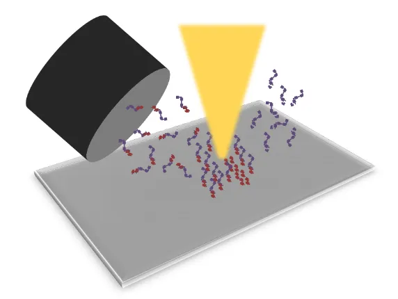
Figure 2.2– During electron beam induced deposition locally supplied precursor gas (red and purple in image) molecules loosely adhere to the sample surface, and are dissociate by incident electrons into a target molecule and a volatile byproduct. The volatile byproduct is removed by the vacuum pump of the system, and the small target molecules are strongly adsorbed onto the sample surface and forms the desired deposit layer.
and 100% purity of gold obtained using electron beam induced deposition techniques. The quality of the deposited material is a critical shortcoming of electron beam induced deposition compared to
other, more established metal deposition techniques like chemical vapour deposition, molecular beam epitaxy, or electron beam evaporation, which are often employed in combination with standard EBL fabrication procedures. As a result, researchers are working to develop methods for achieving higher
quality EBID-deposited materials [89].
In order to improve the quality of the deposited material it is important to understand how the different parameters of the EBID write settings influence the deposition. It is equally important to understand the properties of the deposited material itself, so that its quality can be improved and
fur-ther purified once it has been deposited. Looking at tungsten as a specific example, EBID patterning parameter settings influence the quality of the resulting deposited tungsten material. A first property
of the deposition process that can help with understanding how to improve the writing parameters and deposition conditions relates to the dissociation rate of the precursor gas molecules, which is
proportional to the density of the precursor molecules and EBID electrons at the target substrate surface [90]. The metal content, or purity, of the deposited material increases with increasing beam current, as the higher electron concentration at the target deposition surface leads to more precursor
molecules to be dissociated into a target deposit and volatile byproduct. The size of the deposited nanocrystals formed from the target deposit particles increases with the precursor molecule flux and
resulting concentration [89]. For tungsten obtained fromW(CO)6 precursor gas it was also shown
that the conductivity, which can be seen as an indicator for the deposited tungsten material quality, is increased for slower scan speeds, with longer dwell times and loop times [86] [102]. The above
improvements can be explained by the deposition shifting from an electron-limited to a precursor-limited regime. In the precursor-precursor-limited regime, a larger fraction of the molecules dissociate, and the
will remain adhered to the surface. Although the above findings are described for tungsten, they are more generally valid and are true for several other EBID deposit materials [89].
Looking at post-EBID purification techniques of the resulting material, a first well-known method is annealing: heating up the material can increase the amount of crystallisation of the deposited
material present, and remove impurities from the deposit. However, tungsten in particular is at risk of oxidation, which would decrease the overall metal purity, so the annealing process should take place in high-vacuum conditions, with as little oxygen present as possible to avoid tungsten oxidation.
The impurities in the tungsten material deposited through EBID consist of remnants of undissociated
precursor molecules, molecules for which dissociation was incomplete, byproducts which were trapped on the substrate instead of removed, and residual impurities not removed by the vacuum pump of the system. The residual impurities tend to mostly comprise water vapour, nitrogen, oxygen, and small
hydrocarbon groups, and can be hard to remove once the material is deposited. It would therefore be beneficial to find a method to avoid the impurities and unwanted precursor side products being
deposited in the first place. One potential solution is the technique of reactive gas mixing, the idea of which is to have the impurities interact with a gas added to the chamber, instead of the target
deposit. In the case of gold, which is not oxidisable, adding oxygen improved the deposit material purity, but with easily oxidisable tungsten, the resulting purity was worse than without reactive gases present, as the amount of carbon impurities was not significantly reduced, and the amount of oxygen
contamination increased [103]. It should be noted that in section 2.2.4 tungsten oxide is mentioned as a material which exhibits plasmonic properties, and the oxidation effects mentioned above should
therefore be kept in mind when looking for a method to produce tungsten oxide through W(CO)6
EBID fabrication, as finding good quality precursor gases is not a straightforward task, as those pre-cursors need to be compatible with the EBID system as well as being capable of depositing a target
material with plasmonic properties. In light of the vast array of parameter settings and molecule selections and variations that can be performed, simulation methods have been developed in order to
facilitate a method of predicting outcomes and researching having only the guidance of experimental results [82]. Simulations can also be used to guide determine specific recipe and patterning settings
to achieve desired EBID designs [104].
EBID applications
Van Dorp stated in his 2008 Journal of Applied Physics paper that there are a plethora of results out there [100], and the technology and research community around it have not yet reached a stage
where a common set of results are accepted as tried and tested, illustrating that the technology and field are still in their developing phase. However, the significant benefits and unique fabrication possibilities offered by electron beam induced deposition mean that applications have been achieved
under research conditions for decades. The range of applications explored over the decades is large and includes the creation of field emitter arrays by M orimoto et al. [107] and several conductive nanostructure designs byKoopset al. [108], both in 1996, by depositing platinum or gold on a silicon array using EBID.Graells et al. presented the fabrication of gold plasmonic nanostructures using EBID in 2007 [109]. In 2015,Senguptaet al. published a paper on the fabrication of superconduct-ing tungsten nanowires ussuperconduct-ing EBID [110]. Keepsuperconduct-ing the focus on tungsten, Electron beam induced deposited tungsten obtained from a tungsten hexacarbonyl precursor (W(CO)6) has been used as a