Loss engineered slow light waveguides
L. O’Faolain,1 S. A. Schulz,1 D. M. Beggs,1 T. P.White,1 M. Spasenović,2 L. Kuipers,2 F. Morichetti,3 A. Melloni,3 S. Mazoyer,4 J. P. Hugonin,4 P. Lalanne,4 and T. F. Krauss1,*
1School of Physics and Astronomy, SUPA, University of St Andrews, Fife, KY16 9SS, United Kingdom 2Center for Nanophotonics, FOM Institute for Atomic and Molecular Physics, Science Park 104, 1098 XG,
Amsterdam, The Netherlands
3Dipartimento di Elettronica e Informazione, Politecnico di Milano, Via Ponzio 34/5, I-20133 Milano, Italy 4Laboratoire Charles Fabry de l’Institut d’Optique, CNRS, Univ Paris-Sud, Campus Polytechnique, 91127 Palaiseau
cedex, France
Abstract: Slow light devices such as photonic crystal waveguides (PhCW) and coupled resonator optical waveguides (CROW) have much promise for optical signal processing applications and a number of successful demonstrations underpinning this promise have already been made. Most of these applications are limited by propagation losses, especially for higher group indices. These losses are caused by technological imperfections (“extrinsic loss”) that cause scattering of light from the waveguide mode. The relationship between this loss and the group velocity is complex and until now has not been fully understood. Here, we present a comprehensive explanation of the extrinsic loss mechanisms in PhC waveguides and address some misconceptions surrounding loss and slow light that have arisen in recent years. We develop a theoretical model that accurately describes the loss spectra of PhC waveguides. One of the key insights of the model is that the entire hole contributes coherently to the scattering process, in contrast to previous models that added up the scattering from short sections incoherently. As a result, we have already realised waveguides with significantly lower losses than comparable photonic crystal waveguides as well as achieving propagation losses, in units of loss per unit time (dB/ns) that are even lower than those of state-of-the-art coupled resonator optical waveguides based on silicon photonic wires. The model will enable more advanced designs with further loss reduction within existing technological constraints.
©2010 Optical Society of America
OCIS Codes: (130.5296) Photonic crystal waveguides; (230.5298) Photonic crystals; (230.7370) Waveguides; (290.5910) Scattering, Rough surfaces, (260.2030) Dispersion.
References and Links
1. T. Karle, Y. J. Chai, C. N. Morgan, I. H. White, and T. F. Krauss, “Observation of pulse compression in photonic crystal coupled cavity waveguides,” J. Lightwave Technol. 22(2), 514–519 (2004).
2. A. Melloni, A. Canciamilla, C. Ferrari, F. Morichetti, L. O'Faolain, T. F. Krauss, R. De La Rue, A. Samatelli, and M. Sorel, “Tunable delay lines in silicon photonics: coupled resonators and photonic crystals, a comparison,” IEEE Photonics Technol. Lett. 2, 181–194 (2010).
3. M. F. Yanik, and S. Fan, “Stopping light all optically,” Phys. Rev. Lett. 92(8), 083901 (2004).
4. T. Baba, T. Kawaaski, H. Sasaki, J. Adachi, and D. Mori, “Large delay-bandwidth product and tuning of slow light pulse in photonic crystal coupled waveguide,” Opt. Express 16(12), 9245–9253 (2008).
5. F. Xia, L. Sekaric, and Y. Vlasov, “Ultracompact optical buffers on a silicon chip,” Nat. Photonics 1(1), 65–71 (2007).
6. D. M. Beggs, T. P. White, L. O'Faolain, and T. F. Krauss, “Ultracompact and low power optical switch based on silicon photonic crystals,” Opt. Lett. 33(2), 147–149 (2008).
7. C. Monat, B. Corcoran, M. Ebnali-Heidari, C. Grillet, B. J. Eggleton, T. P. White, L. O'Faolain, and T. F. Krauss, “Slow light enhancement of nonlinear effects in silicon engineered photonic crystal waveguides,” Opt. Express
17(4), 2944–2953 (2009).
9. A. Melloni, F. Morichetti, and M. Martinelli, “Four-wave mixing and wavelength conversion in coupled-resonator optical waveguides,” J. Opt. Soc. Am. B 25(12), C87–C97 (2008).
10. E. Kuramochi, M. Notomi, S. Hughes, A. Shinya, T. Watanabe, and L. Ramunno, “Disorder-induced scattering loss of line-defect waveguides in photonic crystal slabs,” Phys. Rev. B 72(16), 161318 (2005).
11. S. Hughes, L. Ramunno, J. F. Young, and J. E. Sipe, “Extrinsic Optical Scattering Loss in Photonic Crystal Waveguides: Role of Fabrication Disorder and Photon Group Velocity,” Phys. Rev. Lett. 94(3), 033903 (2005). 12. S. G. Johnson, M. L. Povinelli, M. Soljacic, A. Karalis, S. Jacobs, and J. D. Joannopoulos, “Roughness losses
and volume-current methods in photonic-crystal waveguides,” Appl. Phys. B 81(2-3), 283–293 (2005). 13. F. Morichetti, A. Canciamilla, C. Ferrari, M. Torregiani, A. Melloni, and M. Martinelli, “Roughness Induced
Backscattering in Optical Silicon Waveguides,” Phys. Rev. Lett. 104(3), 033902 (2010).
14. F. Morichetti, A. Canciamilla, M. Martinelli, A. Samarelli, R. M. De La Rue, M. Sorel, and A. Melloni, “Coherent backscattering in optical microring resonators,” Appl. Phys. Lett. 96(8), 081112 (2010). 15. M. Notomi, K. Yamada, A. Shinya, J. Takahashi, C. Takahashi, and I. Yokohama, “Extremely Large
Group-Velocity Dispersion of Line-Defect Waveguides in Photonic Crystal Slabs,” Phys. Rev. Lett. 87(25), 253902 (2001).
16. J. Li, T. P. White, L. O'Faolain, A. Gomez-Iglesias, and T. F. Krauss, “Systematic design of flat band slow light in photonic crystal waveguides,” Opt. Express 16(9), 6227–6232 (2008).
17. M. Notomi, T. Tanabe, A. Shinya, E. Kuramochi, H. Taniyama, S. Mitsugi, and M. Morita, “Nonlinear and adiabatic control of high-Q photonic crystal nanocavities,” Opt. Express 15(26), 17458 (2007).
18. M. Gnan, S. Thoms, D. S. Macintyre, R. M. De La Rue, and M. Sorel, “Fabrication of low-loss photonic wires in silicon-on-insulator using hydrogen silsequioxane electron-beam resist,” Electron. Lett. 44(2), 115–116 (2008). 19. T. P. White, L. O'Faolain, J. T. Li, L. C. Andreani, and T. F. Krauss, “Silica-embedded silicon photonic crystal
waveguides,” Opt. Express 16(21), 17076–17081 (2008).
20. L. C. Andreani, and D. Gerace, “Light-matter interaction in photonic crystal slabs,” Phys. Status Solidi, B Basic Res. 244(10), 3528–3539 (2007).
21. Here α is defined as <lnT> = -αL, with <lnT> the ensemble-averaged logarithm of the transmission, which is valid both in the ballistic and the multiple scattering regime [24].
22. M. Patterson, S. Hughes, S. Schulz, D. M. Beggs, T. P. White, L. O'Faolain, and T. F. Krauss, “Disorder-induced incoherent scattering losses in photonic crystal waveguides: Bloch mode reshaping, multiple scattering, and breakdown of the Beer-Lambert law,” Phys. Rev. B 80(19), 195305 (2009).
23. A. Petrov, M. Krause, and M. Eich, “Backscattering and disorder limits in slow light photonic crystal waveguides,” Opt. Express 17(10), 8676–8684 (2009).
24. S. Mazoyer, J. P. Hugonin, and P. Lalanne, “Disorder-Induced Multiple Scattering in Photonic-Crystal Waveguides,” Phys. Rev. Lett. 103(6), 063903 (2009).
25. S. G. Johnson, and J. D. Joannopoulos, “Block-iterative frequency-domain methods for Maxwell's equations in a planewave basis,” Opt. Express 8(3), 173–190 (2001).
26. B. Wang, S. Mazoyer, J. P. Hugonin, and P. Lalanne, “Backscattering in monomode periodic waveguides,” Phys. Rev. B 78(24), 245108 (2008).
27. G. Lecamp, J. P. Hugonin, and P. Lalanne, “Theoretical and computational concepts for periodic optical waveguides,” Opt. Express 15(18), 11042–11060 (2007).
28. The code written by D. M. Beggs and S. A. Schulz is available for free at: www.st-andrews.ac.uk/microphotonics
29. D. Marcuse, “Mode conversion caused by surface imperfections of a dielectric slab waveguide,” Bell Syst. Tech. J. 48, 3187–3215 (1969).
30. L. O'Faolain, T. P. White, D. O'Brien, X. D. Yuan, M. D. Settle, and T. F. Krauss, “Dependence of extrinsic loss on group velocity in photonic crystal waveguides,” Opt. Express 15(20), 13129–13138 (2007).
31. L. O'Faolain, X. Yuan, D. Mcintyre, S. Thoms, H. Chong, R. M. De La Rue, and T. F. Krauss, “Low-loss propagation in photonic crystal waveguides,” Electron. Lett. 42(25), 1454–1455 (2006).
32. S. A. Schulz, L. O'Faolain, D. M. Beggs, T. P. White, A. Melloni, and T. F. Krauss, “Dispersion engineered slow light in photonic crystals: a comparison,” J. Opt. 12(10), 104004 (2010).
33. A. Gomez-Iglesias, D. O’Brien, L. O’Faolain, A. Miller, and T. F. Krauss, “Direct measurement of the group index of photonic crystal waveguides via Fourier transform spectral interferometry,” Appl. Phys. Lett. 90(26), 261107 (2007).
34. J. Topolancik, B. Ilic, and F. Vollmer, “Experimental Observation of Strong Photon Localization in Disordered Photonic Crystal Waveguides,” Phys. Rev. Lett. 99(25), 253901 (2007).
35. R. J. P. Engelen, D. Mori, T. Baba, and L. Kuipers, “Two Regimes of Slow-Light Losses Revealed by Adiabatic Reduction of Group Velocity,” Phys. Rev. Lett. 101(10), 103901 (2008).
36. S. Mazoyer, P. Lalanne, J. C. Rodier, J. P. Hugonin, M. Spasenovic, L. Kuipers, D. M. Beggs, and T. F. Krauss, “Statistical fluctuations of transmission in slow light photonic-crystal waveguides,” Opt. Express 18(14), 14654– 14663 (2010).
37. M. L. M. Balistreri, H. Gersen, J. P. Korterik, L. Kuipers, and N. F. van Hulst, “Tracking Femtosecond Laser Pulses in Space and Time,” Science 294(5544), 1080–1082 (2001).
38. M. D. Settle, R. J. P. Engelen, M. Salib, A. Michaeli, L. Kuipers, and T. F. Krauss, “Flatband slow light in photonic crystals featuring spatial pulse compression and terahertz bandwidth,” Opt. Express 15(1), 219–226 (2007).
1. Introduction
The ability to slow down light in high refractive index contrast nanophotonic waveguides has inspired many applications, such as dispersion compensation [1], optical delay lines [2–5], miniaturised switches [6] and enhanced nonlinear optics [7–9]. While photonic wires and photonic crystal waveguides (PhCWs), the main building blocks of nanophotonic slow light structures, are intrinsically lossless, their performance is limited by fabrication imperfections such as sidewall roughness and lithographic inaccuracies, the high refractive contrast (Δε~10) being responsible for the scale of this problem.
Backscattering loss, in particular, has been recognised as a serious problem in slow light photonic crystals, with an ng2 scaling predicted and observed [10,11]. The ng2 scaling arises as
a consequence of the increased density of states in both forward and backward propagating modes. In fact, backscattering due to disorder is an issue for any type of waveguide [12], as has recently also been shown in nanowires [13] and micro ring resonators [14]. Clearly, if the
ng2 scaling applies as generally as hitherto assumed, it will limit slow light devices to very
short lengths or to moderate group indices only, unless major technological advances can be achieved.
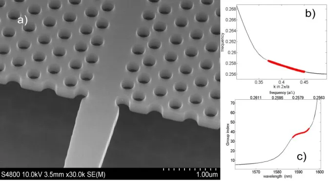
Fig. 1. a) SEM Micrograph of a photonic crystal waveguide. The waveguide is formed by a missing line of holes in a photonic crystal lattice and referred to as a W1 waveguide. The specific waveguide shown here is designed to operate in the mode anticrossing regime [15] and has been dispersion-engineered by symmetrically shifting the two rows of holes nearest to the line defect [16]. b) Corresponding dispersion curve and c) group index vs. wavelength curve. The frequency range of 0.256c/a < ν < 0.258c/a (where a is the lattice period) of nearly constant slope in b) corresponds to the “plateau” of nearly constant group index between 1587nm < λ < 1595nm in c).
Considerable effort has been devoted to realising the technological advances that have led to the current record losses of 2dB/cm for photonic crystals [17] and 1dB/cm for photonic wires [18]. Typical values for the disorder are now on the order of σ = 2nm RMS or better [19], a value that is close to the lattice constant of silicon (0.5nm). Figure 1a) shows an SEM micrograph of a photonic crystal waveguide as an example of a slow light waveguide, highlighting the technological quality that has already been achieved. This suggests that the limits of the current technology are being approached and that it will be difficult to achieve further substantial improvements in fabrication quality.
Finding a design-route to reducing propagation oss is therefore highly desirable and in this paper, we describe such a route. We will show that while the ng2 scaling is fundamental, the
[image:3.612.139.477.261.446.2]2. Theoretical model
It is reasonable to assume, as also proposed by others [12,20], that the loss is composed of two components: the out-of plane radiation losses and the backscattering losses. The former depend linearly on the group index, whilst the latter depend on its square. Using appropriate scaling factors c’1 and c’2, the loss can then be expressed as follows [21],
2
1 2
' g ' g . c n c n
(1)
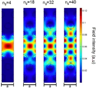
Equation (1) provides a good starting point, but it does not capture the full picture, as it includes the implicit assumption that the mode shape is independent of the group index. While this is a good approximation for photonic wires, it does not hold for photonic crystal waveguides, which exhibit a strong dependence of the mode shape on the group index [22,23]. This effect can be seen in Fig. 2 which illustrates the changes in mode shape calculated for the waveguide shown in Fig. 1a for several different group indices. The mode shape is a critical parameter when considering losses, as it determines the field strength on the sidewall of the holes, which, in turn, determines the fraction of the field available for scattering at imperfections. This dependence can be explicitly included in the theoretical model by introducing the parameters γ = γ(k) and ρ = ρ(k) which describe the mode shape contribution to radiation loss and backscatter loss, respectively;
2
1 g 2 g .
c n c n
(2)
The coefficients c1 and c2 now solely describe the technological parameters, and as shown
[image:4.612.223.396.352.508.2]in [24], contain the dielectric contrast Δε and the disorder parameter σ. The separation of disorder and mode shape contributions in Eq. (2) is very informative and instantly suggests the possibility of addressing the loss-issue by suitably tuning the mode shape.
Fig. 2. Modal field intensity as a function of group index for the waveguide with dispersion shown in Fig. 1b. The fields were calculated as a function of wavevector modulus |k| using 3D MPB [25] and mapped onto group indices via the dispersion curve.
The derivation of ρ in Eq. (2) is based on the Lorentz reciprocity theorem, which treats scatterers as radiating dipoles [26]. Following this model, radiation scattering and backscattering need to be treated differently; radiation loss occurs into a continuum of radiation modes, whereas backscattering occurs into a single mode only, i.e. the guided mode of the system propagating backwards. Therefore, the mode shape dependent backscattering parameter is given by [26]:
2
-1 1 2
( ) d ,
c
n L
where we have made the assumption that the disorder only occurs at the etched side-walls. Lc
is the correlation length (see below) measured along the boundary of a hole, and the hole boundaries are broken up such that there are n parts of length Lc in one unit cell (distributed
over all the holes in a unit cell). ET is the electric-field component tangential to the hole
surface and DN is the displacement-field component normal to the hole surface; note that the
complex components ET and DN are continuous across the interface. ε1 and ε2 are the two
dielectric constants constituting the photonic crystal, i.e. that of the matrix and that of the hole.
Deriving a similar exact analytical expression for the out-of-plane coefficient γ, is more challenging, as it involves the coupling between a guided Bloch mode and the continuum of radiation modes. This is difficult to implement due to the large number of modes required to simulate the radiation continuum. By way of approximation, we therefore treat the disorder as again creating local dipole sources, in agreement with the derivation of ρ. By assuming wavelength and position independent coupling of the dipole radiation to the air-mode continuum, we obtain:
2 1
d ,
c
n L
ET D rN (4)where ε1 is the dielectric constant of the material at position r, an expression that takes
local-field corrections [12,26] and the local phases of ET and DN into account [27].
In order to implement this calculation we have calculated the complex field amplitudes
E(r) and D(r) using the freely available MIT Photonics Band (MPB) code [25], which is a 3D plane-wave method that uses periodic boundary conditions to calculate the eigenfrequencies and eigenmodes of our PhC waveguides. The field profiles (or eigenmodes) are calculated on a cubic grid of points separated by a/16, and the surface integral along the hole boundaries then proceeds by splitting the unit cell into horizontal slices and interpolating the fields between the grid points on the edges of the holes, using one point per degree of arc. One may be concerned that interpolating the fields near a dielectric boundary could introduce numerical instabilities, but note that we are only concerned with ET and DN. These two components of
the field are continuous at a dielectric boundary, and so the interpolation is numerically robust. The fields are normalized for every k-point (see [25]), and the ng-dependence of the
propagation loss is then inserted explicitly into Eq. (2). We believe that this notation is clearer than the alternative of including ng directly as a parameter into γ and ρ as in [26]. For more
information on the implementation and the code used see reference [28].
Correlation length
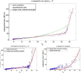
A closer examination of the numerical evaluation of Eq. (3) yields one of the key insights of the paper, and helps us to understand the correlation length of the imperfections that cause extrinsic loss. Disorder is normally described by a correlation length [29] – the distance over which the occurrence of defects is correlated to one another. For distances shorter than the correlation length, the electric fields in Eqs. (3) and (4) should therefore be added coherently. To illustrate the impact of the correlation length on ρ, we show a plot of ρvs. ng in Fig. 3 that
includes the effect of the mode shape variation from Fig. 2. The simplest model is to assume a correlation length approaching zero, such that each scatterer acts independently. The integral in Eq. (3) then reduces to assessing ET.ET and DN.DN on each point of the hole boundary and
adding the resulting values incoherently. This approach is similar to the one chosen by Petrov
et al. [23] and yields the green dashed curve in Fig. 3.
Fig. 3. Backscattering coefficient ρvs. group index. The solid red curve represents ρ given by Eq. (3) with the integration performed over an entire hole boundary, while the green dashed curve corresponds to point-by point addition, which assumes scatterers to be independent. The black dot-dashed curve corresponds to a correlation length of 40 nm, which is also not able to represent the observed strong increase of backscattering for higher group indices shown in Fig. 4.
If, however, we integrate over the entire circumference of the hole, we obtain the red solid curve, which predicts a dramatically different loss behavior when compared to the first two curves. In particular, the backscattering coefficient initially decreases with increasing group index up to ng~40 then increases rapidly beyond ng~40; much faster than either of the other two models. As such clear differences arise from the choice of correlation length, it is relatively easy to compare the predictions against experimental data and determine which model of disorder is most appropriate. In section 3 we show that the third option – integrating coherently over the entire circumference of the hole – provides an excellent fit with experimental loss measurements on several different waveguide geometries (Fig. 4). The good agreement suggests that the correlation length in photonic crystals is larger than previously assumed and that it extends over the entire hole. Furthermore, it implies that the loss mechanism is not simply roughness scattering as in photonic wires, but that it is a combination of roughness, radius and hole position disorder. It is difficult to separate these three effects further at this point, as roughness on the hole sidewall can also appear as a form of radius disorder in the experiment – the important thing is to add any such scattering
coherently along the surface of the entire hole. For comparison, it is interesting to consider the following formula, which has, effectively, been used previously to calculate ρ [22,30] but which excludes phase/coherence effects by taking the modulus of the respective fields before integrating:
2 2
2 2
1 1
* *
1 2 1 2
. . d d ,
b b
H H
E ET T D DN N r
ET DN r (5)where Hb is the hole boundaries in a unit cell. Using Eq. (5) results in a curve that has an
identical ng dependence as that of the point scatterer assumption (dashed green in Fig. 3). A
3. Experimental data
Photonic crystal waveguides with a = 410nm lattice period and radius 0.270a were fabricated on a SOITEC silicon-on-insulator wafer with a nominally 220 nm thick silicon guiding layer on a 2000 nm layer of buried oxide. The pattern was defined in 350 nm thick ZEP-520A electron beam resist using a VISTEC VB6 electron beam writer with a 1.2 mm writing field and an acceleration voltage of 100 kV. The pattern was transferred into the silicon layer using reactive ion etching (RIE), with a combination of CHF3 and SF6 gases, before selectively
[image:7.612.172.456.230.486.2]removing the buried oxide using hydrofluoric acid wet etch. The fabrication process is based on that reported in [31] and has been carefully optimized to yield devices with state-of-the-art disorder levels (below 2 nm RMS [17]) and is known to yield low-loss PhC waveguides with losses of 5 dB/cm or better in the fast light regime (Fig. 4). Coupling regions, as described in [32] were used to aid coupling of light into the slow light regime. The experimental group index is measured by Fourier-transform spectral interferometry [33].
Fig. 4. Loss vs. group index for different waveguide designs. The losses were extracted from transmission measurements of waveguides ranging between 180 um and 2000 um in length. a) Waveguide designed to exhibit a constant group index of ng38 over a Δλ8nm wavelength range (s1 = 48nm, s2 = 16nm) [16]. The green dashed curve is the best fit according to Eq. (2) with losses assessed point by point, while the red solid curve assumes a coherence length equal to the entire hole.b) Waveguide designed to have a constant group index of ng27 over a
Δλ10nm wavelength range (s1 = 52nm, s2 = 0nm). c) Standard W1 waveguide (s1 = s2 = 0nm). Identical values of c1 and c2 (2cm1 and 110cm1 respectively) were used for all three waveguides.
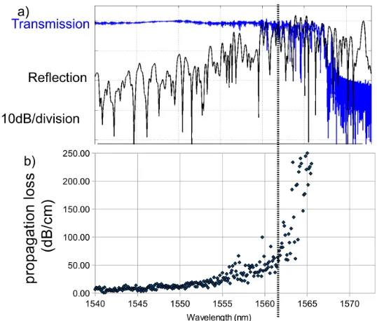
In order to examine separately the contribution of radiation and backscattering to the loss and thereby verify our model, we measured the waveguide directly in transmission and reflection. The result is shown in Fig. 5. For low group indices, the reflected signal is weak – more than 20 dB below the transmitted signal - indicating low backscattering. Once the group index increases to ng35, however, the two signals become comparable, implying that
dependence below ng35 is caused by the suppression of backscattering losses, while the
sudden increase of the backscattering shown in Fig. 3 is responsible for dramatic increase in loss around ng38.
Fig. 5. a) Transmitted and reflected power directly measured through a dispersion engineered waveguide of 180µm length. The transmission signal is normalised to a PhC waveguide in the fast light regime, thus accounting for the insertion loss. b) The loss-measurement from Fig. 4 (a), plotted against wavelength is included for comparison. The black dotted line corresponds to ng38
4. Multiple Scattering
In the past multiple scattering has been recognised as a problem for slow light PhC waveguides [22,24]. Here we investigate this phenomenon and present near field optical measurements in support of our model. Multiple scattering occurs when light is not backscattered once, but multiple times, with the result that characteristic hot-spots form along the waveguide [34–36]. The lateral extent of these hot-spots indicates the localisation length. If the localisation length is shorter than the device length, then multiple scattering will impact on device operation and propagation can no longer be described by the “ballistic” transport of photons [22,24,36]. To study multiple scattering in dispersion engineered waveguides, we investigated a similar waveguide to the one shown in Fig. 1(a), except that it was deliberately “overengineered” to the extent that the group index reached ng100 in the anticrossing region.
This design was chosen to accentuate the differences between the anticrossing regime and the band-edge regime, providing a direct visual comparison up to group indices of ng100 in the
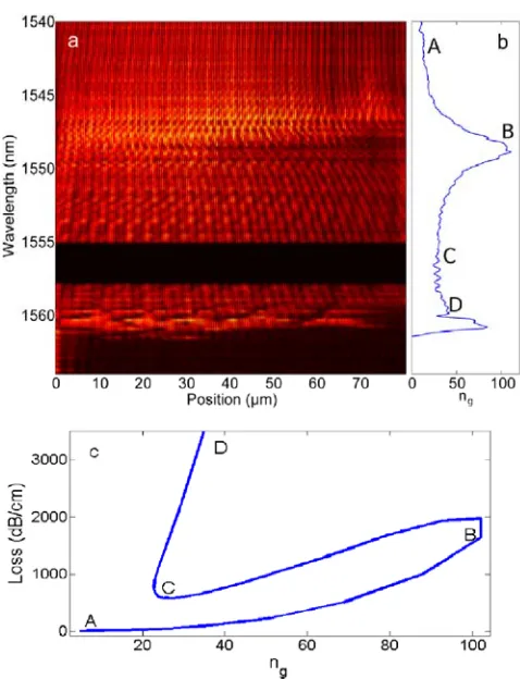
[image:8.612.172.441.111.340.2]Fig. 6. a) Scanning near field optical micrograph of the amplitude of the electric field. The figure is a montage of scans along the same waveguide taken at different wavelengths. No measurements were taken in the black region between 1555nm and 1557.5nm b) Corresponding experimentally-measured group index curve c) Calculated loss curve clearly highlighting the difference between anticrossing and bandedge slow light. Significantly, anticrossing slow light at point B achieves significantly higher group indices with lower losses than bandedge slow light at point D.
This measurement was performed using a scanning near-field microscope (SNOM) [37]. TE-polarized light from a continuous-wave tunable laser source is injected into the PhC waveguide and an aluminum-coated near-field tip with an aperture diameter of 200nm is scanned over the sample at a distance of 20nm. By mixing the light picked up by the tip with a frequency-shifted reference beam of known linear polarization, the amplitude, phase and polarization of the evanescent electric field can all be measured simultaneously with a heterodyne detection scheme. The tip is scanned along the entire length of the waveguide, above the waveguide axis. The measurement was repeated at wavelengths from 1540nm to 1555nm and 1558nm and 1564nm in steps of 0.2nm.
[image:9.612.190.429.70.382.2]localisation. With a further increase in wavelength (C in Fig. 6), the group index decreases again and the more uniform distribution is regained. Note that the slow modulation, due to interference of forward- and backward-propagating Bloch components, now becomes more widely spaced (approximately 10 lattice spacings), as is characteristic for Bloch modes close to the bandedge due to the magnitude of the wavevector difference between the forward- and backward-propagating components decreasing when the bandedge is approached. As the wavelength comes close to the bandedge (D in Fig. 6), the amplitude pattern changes again. We observe a rise in amplitude, accompanied by a large number of random hotspots which are smaller in size than the hotspots observed in the anticrossing regime, indicating strong localization and multiple scattering [34].
Using our model, we can predict the corresponding loss for the waveguide, shown in Fig. 6(c). It should be noted that as our model is based on perturbation theory, it cannot quantitatively predict the occurrence of multiple scattering. However, as multiply scattered light is a subset of backscattered light, we can place an upper limit on the amount of multiple scattering that occurs. In essence, regions of weak backscattering cannot exhibit strong multiple scattering.
The comparison between the anti-crossing regime (B) and the bandedge regime (D) is very informative. Near the band edge, extremely high loss (predominantly backscattering) is predicted, in excellent agreement with the short localisation length and the many localisation hotspots observed. In the anti-crossing regime, the predicted loss is orders of magnitude lower leading to multiple scattering with very long localisation lengths and fewer localisation hotspots. It is also interesting to note that a much higher group index is measured in the anti-crossing regime (see Fig. 6(b)) by virtue of the stronger transmission.
The good agreement between model and experiment allows us to draw two important conclusions. The first is that our model is able to qualitatively explain the onset of multiple scattering via the backscatter coefficient; if the backscatter coefficient is larger, the multiple scattering regime is entered for lower group indices. The second is that in the anticrossing regime, multiple scattering plays a much smaller role than in the bandedge regime, so multiple scattering cannot be held responsible for the sudden onset of loss shown in Fig. 4(a).
5. Discussion
The motivation for the structural modification applied to the photonic crystal waveguides described in this paper (Figs. 1 and 4) was initially to engineer their dispersion and to achieve a flatband region of constant group index. It is now clear, however, and much better understood, that the dispersion engineering also leads to loss engineering via the modification of the modal field distribution and the backscatter coefficient ρ. For example, these loss and dispersion engineered devices have already demonstrated their superiority over standard photonic crystal waveguides, both with respect to propagation loss and group index bandwidth product, by enabling the enhancement of nonlinear effects [7,39] and the demonstration of high bit-rate (100Gbit/s) delay lines with lower loss than those based on silicon wires [2]. The latter point is particularly noteworthy and has already been pointed out in [32], where we have highlighted the importance of the loss per unit time in dB/ns as the figure of merit for slow light waveguides. Clearly, if the objective is to slow light down and to store it in the structure for a given period of time, then the loss per unit time is the important parameter and the loss per unit length becomes less relevant. Consequently, when comparing the loss per unit time, we have noticed that our dispersion/loss engineered structures offer the lowest value for any high refractive index contrast structure. The best losses for microring-based coupled resonator optical waveguides in silicon are in the range of 44-60 dB/ns, while our photonic crystal waveguides achieve 25-40 dB/ns [32].
possible without understanding the loss issue and describing it by the comprehensive model as we have done here. Both examples also demonstrate that further improvements in the performance of photonic crystal based devices are possible that do not require improvements in the fabrication processes.
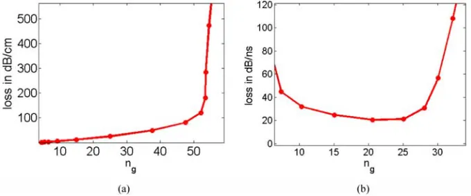
Fig. 7. a) Calculated loss curve for s1 = 0.10a, s2 = 0.05a and r = 0.286a. The curve shows that the propagation loss can be kept linear with respect to ng for group indices in excess of 50. b) Calculated loss per unit time for a structure with s1 = 0.10a, s2 = 0.08a, r = 0.286a and r2 = 0.240a highlighting that the loss per unit time can be reduced further (20dB/ns). Where s1 and
s2 are the lateral shifts of the 1st and 2nd row respectively and r2 is the radius of the second row, following [32].
Conclusion
We have developed a new understanding of the origin of extrinsic losses in slow light structures based on high contrast waveguides, especially silicon photonic crystal waveguides. More importantly, we have developed a new model that can guide new designs that should exhibit even lower losses without having to improve the fabrication technology. The model is a simple perturbation model based on the Lorentz reciprocity theorem that treats scatterers as radiating dipoles and is able to fully describe the complicated loss-dependence observed experimentally for structurally engineered slow light waveguides. These waveguides have proven to be a very good model system for studying slow light-related losses in general by allowing us to gain a clear understanding of the physical mechanisms involved. We have clarified the balance between radiation and backscatter losses and shown that the impact of the latter can be reduced significantly by appropriate design, at least within a limited operating window.
The work proves that the technological parameters and group index alone are insufficient to describe the loss-dependence of a particular type of waveguide, and that the mode shape has a significant impact on losses. This observation is in agreement with previous work [22,23] but we add the key point that phase, via the coherence length, matters more than previously assumed. We show that scattering across an individual hole adds coherently, while scattering from neighbouring holes adds incoherently, i.e. the coherence length is given by the circumference of the hole. This is a key aspect as it leads to a reduction of the backscattering coefficient ρ with increasing group index, which allows the reduction of propagation loss through appropriate waveguide design.
[image:11.612.135.475.130.272.2]Acknowledgments