UNIVAC
®
CALCULATING TABULATOR PROCESSOR MANUALSECTIONS: APPENDIX:
"
4 & 5
C
COM PAN
yeo
NFl
DENT I A L
REGISTERED CIRCULATIONcoPY
#:10
The information contained in this manual is the property of the Sperry Rand Corporation and is Company Confidential. It is submitted in confidence and should not be disclosed to others unless so disclosed in confidence with the per-mission of Remington Rand Univac, Division of Sperry Rand Corporation, being first obtained. This copy is numbered
and is so registered in your name in our records. The document is not to he reproduced or duplicated without express permission in writing from a duly authorized representative of the Sperry Rand Corporation. This manual is subject to recall.
Par agr aph 4-2
4-5
4-9 4-20 4-40 4-47 4-52 4-54 4-55 4-58 4-61 4-62 4-67 4-70 4-72 4-74 4-77 4-83 4-88 4-92 4-93 4-94 4-96 4-109 4-112 4-116 4-118 4-120 4-127 4-135 4-138 4-139 4-144 4":145 4-150 4-153 4--156 4-115 4-176 4-183 4-184 4-186 4-181 4-188 4-190 4-191 4-192SECTION IV TABLE OF CONTENTS
Title Basic Operation Cycle
Search-for-Instruction Step~
Locating the Memory Address Comparison and Head Selection Band Selection
Staticize-Instruction Step Storing the- p7 Digit
Storing the Instruction Word Staticizing the Instruction Search-for-Operand Step
Instruction Code Characteristics Locating the Operand
Execute-Instruction Step
Two-Execution-Step Instructions Timing of the Basic Operation Cycle Processing a Typical Instruction
Search for Operand
Execu te th e H( 60) Ins_true t ion Memory Write Operation
Arithmetic Operations
Addition and Subtraction Add Instruction
Al Step A2 Step
Sub
t rae t ion' Sample ProblemsAddition Subtraction
M u I tip 1 i cat i o-n
General Description Detailed Description
MI Step M2 Step
IER Phase
i l l
Phase DivisionGeneia! Description Detailed Description 01 Step
D2 Step OR Ph ase.
Complementing and Left Shift of rA Complementing and Left Shift of rX Complementing the LSD
of rA
Jam MQe, _ ~
Initiate
OR Phase
OR
Phase .
4-193 4-194 4-195 4-196 4-199 4-200 4-202 4-206 4-210 4-213 4-217 4-220 4-226 4-228 4-230 4-232 4-235 4-237 "4-243 4-246 4-249 Number 4-1 4-2 4-3 4-4 4-5 4-6 4-7 4-8 4-9 4-10 4-11 4-12 4-13 4-14 4-15 4-16 Number 4-1 4-2 4-3 4-4 Addition
End of D2 Step D3 Step
Interchanging rA and rX Sign of the Quotient Error Circuits
Memory-Check Flip-Flop Timing-Error Flip-Flop
Cycling-Unit Error Flip-Flop Input-Output
Manually-Controlled Operations One-Line Print
One-Card RPU One-Card HSH One Instruction Comparison Stop Keyboard Input Manual Operation Depressing a Key Releasing a Key
Signing and Releasing the Word
ILLUSTRATIONS
Title
Search Step of Basic Operation Cycle Drum Quadrants
Drum Quadrants under Fast-Access Heads Quarter Addition of
QS2 FF
InputsStaticize Step
Timing of Basic Operation Cycle Execute Step of H(60) Instruction Add Instruction . Multiplication Process
Multiply Instruction Division Process Dl Step of Division D2 Step,
Q!
Phase D2 Step. OR Phase D3 StepKeyboard Input Operation
TABLES
Title
Oddness and Evenness of Biquinary Combinations Head Selection
Instruction Code Combinati~ns Keyboard Encoder
/
SECTION
IV
THEORY Of OPERATION4-1. Section II, by explaining the use of logical sym-bols and elements. ~nables the reader to interpret the logical circuitry of the processor. Section III, by describing the logical components of the processor. familiarizes the reader with the specific circuits encountered in this section. section IVt and in the
Analysis of UCT Instructions manual. The purpose of this section is to apply the knowledge gained in the foregoing sections to actual computer operations in which more than just an understanding of the logical circuits is necessary. Types of instructions not de-tailed in this section are treated on the more general
level in section V. All instructions are treated in complete detail in the Analysis of UCT Instructions manual.
4-2. BASIC OPERATION CYCLE
~-a.-
iheb~sic o~eratio~ ~ycle consi~ts
of the steps necessary to perform any instruction completely. All instructions require at least three basic steps.Instructions requiring only three steps are those in which no operand is involved. such as a simple register-to-register transfer. Most instructions. however.
require four basic steps because of the need for an operand. For this reason, a basic operation cycle con-sists of four steps. In instructions requiring only three steps the third or search-for-operand .step is by-passed. The four steps of the normal cycle. with the search for the instruction as the starting point. are:
(1) Search for the instruction (Sc). (2) Staticize the instruction (Sz). (3) Search for the operand (Sc-m). (4) Execute the instruction (Ex).
4-4.
When an instruction is completed, an ending pulse is generated which clears the static register and starts the next cycle by initiating a search for the next in-struction in the program (search for the inin-struction).When an instruction has been located OD the drum it is
read from storage by the read circuits and is stored in the static register and register C (rC) (staticize the instruction).
If
the instruction requires an operand another search is made for this quantity (search for the operand). When the operand is located, the first step of the instruction is executed <execute the instruc~ion).Any further steps in the instruction are executed in order after the first execution step. At the completion of the execution of the instruction, an ending pulse is produced to start the sequence once more.
4-5. SEARCH-FOR-INSTRUCTION STEP
4-6. After an instruction has been completed a signal is applied to the ending pulse buffer of the static register. As shown in figure 4-1. the ending-pulse buffer generates the EP signal which is applied to the restore gates of the seven static-register flip-flops. The high EP signal restores all seven flip-flops to their
barred outputs, which indicate 0 bits at tllB of the execute step of the preceding instruction. The new out-puts of the static register drive the instruction decoder. 4-7. Only the search (5c) gateline of the instruction decoder is permissive to the 0 bits. The search gate interprets the two O's in the two lowest-order bit posi-tions, STRI and 5TR2, and generates the lA function signal. Function signal (FS) IA drives the function en-coder and generates function signals 1, 58+, 63 and 74. These four function signals and FS lA control the
search-for-instruction step.
4-8. In the search-for-instruction step, the storage ad-dress specified by the c adad-dress in rC must be located, the specified band selectedt and the memory-read circuits
alerted to read the instruction word contained in the address.
4-9. LOCATING THE MEMORY ADDRESS. In the search for a memory address the following m~st be determined: the word channel and drum quadrant containing the desired address. the proper band, and the read-write head which is to be energized to read the contents of the location. One of four heads must be selected in reading from a fast-access band. In normal access, however, only one head can be
DRUM MEMORY
c ADDRESS STORED BY PRECEDING INSTRUCTION
END OF PRECEDING INSTRUCTION
TIMING BAND + Alert
,---I
I
Set Flip-Flop7
CP FF
I
---1---,
l
lNITIAL FORCE COMPARATOR IDECIMAL CARRY I
((
,.p(f)e.
~---~I
Memory Address TIMING BAND READ CIRCUITSTS Signals
plO p9 p8 p7 p6 p5 p4 p3 p2 pI
I
I I I
, ~ c Addres.* REGISTER C I I
m
T
I
c
I
CT63 Alerts
c Output Gates
FS63
i
FUNCTION ENCODER
t
FSIA
I
I
I
pI, p2
I
I
~..;..;...----... - - t BiNARY
I
EQUALITY -;;,;I
- GATESI
L-~~I
TS TS
M
BUFFERS p3, MI
I
FF t - -I
I
EQUALITY QUINARY I ~ ~ r - -I
I GATES
I
,...---, pi, p2
~~--+---~---~~
S BUFFERS E
e
Blocks Input From rA
I
L ________________
~p4
~ INSTRUCTION DECODER
I
i
STATlC~EGISTE;-
- - --l-l-j
I
I I
II
l
FF8 FF7 FF6 FF5 FF4 FF2 FFI1
I
I I
I
J~---~---~ lI
Step to SZ Step When Address Located* *
~ r----QUADRANT SELECTION FFI QUADRANT SELECTION FF2 BAND SELECTION FLIP-FLOPS (p3) BAND SELECTION FLIP-FLOPS (p41
I
-J
r--t"'*
m ADDRESS IN SEARCH FOR OPERAND STEPRTS L CIRCUIT
r
-SWITCH SELECTION
-GATING
-MATRIXI
~~D~~~
EPt
t
1
! !
t :
*
*
STEP TO EXECUTE STEP IN SEARCH FOR OPERAND STEPI
BUFFERI
L _______________
~Figure 4-1. Search Step of Basic Operation Cycle
MEMORY READ FROM SWITCHES
-
ADDRESS SELECTEDHEAD -I
Of
450 449
HEAD
00 J.
~o
/
tOO TAddress tt9 HEAD
.0
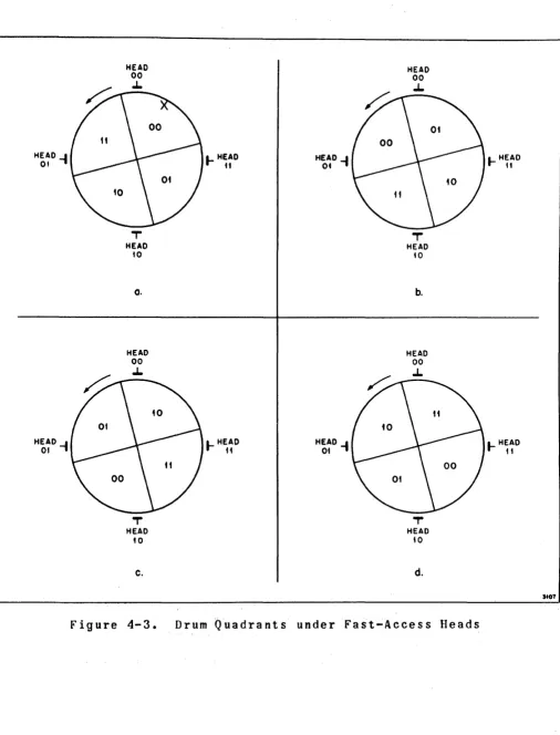
Figure 4-2. Drum
.... HEAD It
310.
selected since there is only one head per track. In a search for an address, the bits of the four c-address digits stored in rC are used as follows:
p4 p3 p2 pI
x ,xxx ~ xx ,X) ~lxXX XXXX)
y y
I
I
Iselect one of I select 4 of 200 25 bands I channels around
I
the drumselect one
of four
ch
anne 1 s. quadrantst and heads4-10. Because there are four heads spaced at 90 degree intervals around the drum in fast~~ccess storage, it is necessary to theoretically divide the surface or circum-ference of the drum into quadrants. It is necessary to refer to quadrants in normal access because both types of access storage use the same circuits. One of the four fast-access heads must be energized to read- or write at the time the quadrant containing the desired memory address is approaching that head, minimizing the time required to read from or write onto the drum.
4-11. The pI digit and the three lowest-order bits of p2 partially represent the channel across the drum in which the correct address is found. If the complete
address is 4469t pI represents the 9 digit. However, the
3 lowest-order bits of p2 do not fully represent the 6 digit; they merely show that the digit is either 1 or 6. Since addresses 000 through 199 are found within a band, the word can be in anyone of channels 019. 069. 119, or 169. These four possible combinations for the time sel-ection bits are shown in figure 4-2. The most signifi-cant bit (MSB) of p2 and the MSB and least signifisignifi-cant bit (LSB) of p3 choose one of the quadrants, completing the selection of a channel, and also selecting the head to be energized for reading. The remaining bits of digit p3 and the bits of digit p4 seleet the proper band.
4-12. Digit p2 of 4469 is 6.1001 in biquinary code. The three lowest-order bits, 001 t are common to both 1 and 6
in biquinary code. Therefore if the MSB of p2 is a 0. the address is either 019, or 119; if it is a I, the address is either 069 or 169. In address 4469 the MSB of p2 is 1; therefore the address is in either quadrant 01 or 11 (addresses 169 or 069) as shown in figure'4-3.
Table 4-1. Oddness and Evenness of Biquinary Combinations
Biquinary Code MSB LSB
O' 0 0 0
0 0 0 1
o
0 1 00 0 1 1
p3---> 0 1 0 0
1 0 0 0
1 0 0 1
1 0 1 0
1 0 1 1
1 1 0 0
Decimal Equivalent
o
1
2
3
4
5
6
7
8
9
a
o
=
even; I = oddEven or Odd a
MSB LSB
o
and 0=
0o
and 1=
Io
and 0=
0o
and 1=
1o
and 0=
0 I and 0=
1 1 and 1 = 01 and 0 = 0
1 and 1
=
0 1 and 0::: 14-13. Address 069 has an even-hundreds digit; address 169 has an odd-hundreds digit. The least-significant bit of p3 designates one of the two quadrants selected
HEAD
-I
OfHEAD
-I
01
4-8
HEAD
00
J.
T
HEAD
to
o.
HEAD
00
J..
T HEAD
to
c.
I-
HEAO itI-
HEADit
HEAD
-I
OtHEAD .-I 01 .,
HEAD
00
J..
T
HEAD
to
b.
HEAD
00
J.
T
HEAD
10
d.
Figure 4-3. Drum Quadrants under Fast-Access Heads
I-HEAD H
[image:10.613.39.545.51.715.2]GATE 31A
S4-0~
51 -t--.r-IJ-,
Mt
°
J-t
A 0
S4-i~1
S1
o.r J
-GATE 378 -
Mt
0
' ] -,
A 0
GATE 37C
S4-0~
St-O--.r-°J-Mt
, 1 ) - ,
A 0
S4-'~0
St,.r J
-GATE 37H ' ]
-Mt I t
A 0
A PRESENT (LOW)
~-I~t
SI
O.r J
-GATE 370 O J
-MI t t
A I
GATE 37E
S4-0~
Sf
-t--.r-tJ-M~
1 °J-I
A t
GATE 31F
S4-0~
51
-O--.r-°J-0
~
0 ] - ,A I
S4-t~0
SI I .r J
-GATE 37G -
0]-MI 0 ,
A ,
A PRESENT (LOW)
Figure 4-4. Quarter Addition of QS2 FF Inputs
[image:11.615.65.567.61.700.2]4-14. This combination of the MSB and LSB of p3 is neces-sary because the least-significant bits of the biquinary code do not form a pattern by which the oddness or evenness of a digit can be determined. The first column of table 4-1 shows that the LSB of p3 (0), if taken alone could indicate either an odd or even decimal digit. The last column shows that by combining the LSB and MSB of the
combinations for each digit, a definite pattern is formed. When the combined bits equal 0, the digit is even; when they equal 1. the digit is odd.
4-15. In the 4469 address digit, p3 is 0100 (4) which is an even-digit combination (0). Therefore digit p3 signifies that the address is contained in a location
having an even hundreds digit, such as ~69, ~69. 169, ~69,
or ~69. The MSB of p2 already has designated either the
16q or 069 channel. The p3 digit, being even, specifies the 069 channel and therefore quadrant 01.
4-16. The MSB of p2 and the LSB of p3, both of which determined the correct quadrant, also select one of the four heads in a fast-acces9 band. With the 000 address in a band under the 00 head, the four quadrants and four heads are as shown in figure 4-2. To determine the head to be energized. the MSB of p2 and the LSB of p3 from rC and the timing combination from memory are quarter
added. Table 4-2 lists the possible combinations of these bits. The four conditions shown under table 4-28 refer to the drum position in figure 4-3a; that is, quadrant 00 is under head 00. The conditions under table 4-2b refer to the possible conditions when quadrant 01 is approaching head 00. Similarly, table 4-2c and figure 4-3c show the
possi-ble conditions when quadrant 10 is approaching head 00; table 4-2d shows the possible conditions when quadrant 11 is approaching head 00.
4-17. The cutaway view of the drum in figure 4-4a shows the conditions specified in table 4-2a. It must be remem-bered that the quadrant called for in the c address is represented by the two quadrant selection bits of re. that is, the MSB of p2 and the LSB of p3. If the 00 quadrant is under the 00 head, as in all four eases of table 4-2a, and the 00 quadrant is called for by re, combination of the two quadrants results in selection of the 00 head. If
the desired address is X in quadrant 00, the 00 head must be selected as the drum rotates in a counterclockwise dir-ection. If the drum quadrants are in the same position and quadrant 11 is specified in the c address, the 01 head must be selected.
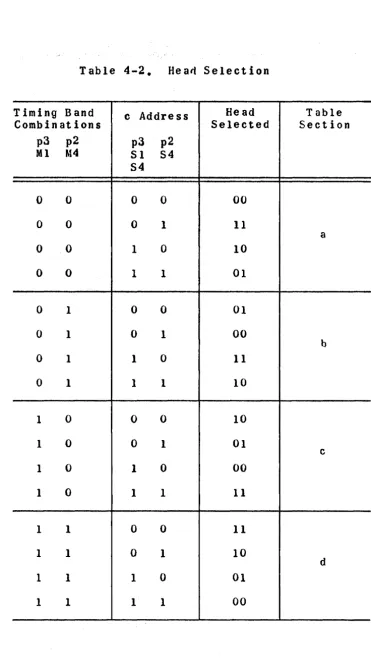
Table 4-2. Hea~ Selection
Timing Band c Address Head Table
Combinations Selected Section
p3 p2 p3 p2
Ml M4 51 54
54
0 0 0 0 00
0 0 0 1 11
a
0 0 1 0 10
0 0 1 1 01
0 1 0 0 01
0 1 0 1 00
b
0 1 1 0 11
0 1 1 1 10
1 0 0 0 10
1 0 0 1 01
c
1 0 1 0 00
1 0 1 1 11
1 1 0 0 11
1 1 0 1 10
d
1 1 1 0 01
[image:13.617.140.511.64.731.2]4-18. With any of the other three quadrants under the
00 head, as in figure 4-3a, 4-3b and 4-3c, head selec-tion again depends on the quadrant to be read. For example, in figure 4-3c, the 10 quadrant is under the
00 head. Therefore, if the 11 quadrant is to be read, the 11 head. which is most immediately in the path of counterclockwise rotati~n of the drum and quadrant 11,
is selected. The same conditions ia table 4-2c_ (last line) verify the head selected in figure 4-3c.
4-19. Thus far, digits pI, p2. and part of p3 have selected the proper memory channel, the quadrant con-taining the address, and one of four heads to be ener-gized in reading that address. Digit p3 and the three LSB's of p4 determl~e which of five fast-access bands
contain the address. Digit p3 determines the third digit, the hundreds digit, of the address; the three
lowest-order bits of p4 determine the fourth, or thousands digit of the address. A detailed explanation of the memory search process is given in paragraph 4-20.
4-20. COMPARISON AND HEAD-SELECTION. The comparison operation (figure 4-1) begins with the comparison of the timing band channel addresses with the address contained in rC. As shown in the figure. the timing band signals enter the comparator on the M lines from the M buffers; the c-address signals from rC enter on the S lines from the S buffers. (Figure 4-1 and the logical diagrams in Appendix A are pertinent throughout this description.) 4-21. Function signal 63 alerts the c-address outp~
gates of rC. The gates are made permissive by the CT signal from the condition~ transfer flip-flop (CT FF). The CT FF is restored to CT by the RCT outputs of the
static register at the end of every search operation. Digits pl. p2. and p3 of the c address in. rC are
transferred, through the permissive output gates, to the S buffers. The p4 digit goes directly from rC to the band-selection flip-flops. The output signals of the four output gates of rC (figure A~l) are C12, C22, C32. and C42. The c address from rC can enter the S buffers and the S lines because ,FS 58+ has blocked the
(rA) outputs which normally enter the S buffers. The pI and p2 digits of the e address are transferred on the S lines into the quinary and binary equality gates of the comparator.
4-22. Function signal 1 alerts the input gates of the M buffers from to to t2B. The timing band combinations signals T51 through T54 from the timing-band read circuit enter the M buffers and the M lines.
4-23. Function signal 74 sets the complement (CP) FF of the sign-and-control circuit to produce a complement (CP)
signal for the comparison operation. The CP signal alerts the binary and quinary equality gates of the comparator. Function signal 74 also generates a CP5 signal from the CP FFfor use in the comparison operation. The CP5 signal drives the initial force~decimal-carry circuit which
generates the A and C decimal-carry signals. These signals alert the quinary equality gates and binary carry gates of the computer.
4-24. The pI digits from rC and memory arrive on the M and S lines at time tiB. The quinary bits of pI (MI. M2. M3. and Sl. 52. 53) are compared in the quinary equality gates of the comparator. Equality between the three M bits and the three S bits makes one of the eight gates
permissive and causes a high output from one of the quinary equality gates. The high output goe~to a non-complement-ing amplifier which produces a high EQ output at t2B.
4-25. Before the comparison operation at tilB of the previous word time the time selection flip-flop (T5 FF) (figure 4-1) was set. The set state of the TS FF indi-cates equality of the M and 5 bits. Inequality of the M and 5 bits restores the TS FF. indicating that the timing-band address under the T5 head at that instant does not match the c address in rC. At various times the T5 output is sampled to see whether a match has been obtained. Restoring the TS FF causes another search cycle to be initiated at the time TS is sampled. If the flip-flop remains set. it indicates equality of the
tim-ing address bits with the c-address bits. The TS FF input gate~l (figure A-12) restores the flip-flop to TS only when EQ is low at time t2B or t3B. The EQ output is low only when the quinary bits are unequal, resulting in
~low output from the quinary equality gates. The high
EQ signal blocks input gate 21 to keep the T5 FF seto
amplifier to generate a high
AT
at t2B. This indication of equal binary bits ~esto gate 20, an input gate of the T5 FF. The high At signal blocks the gate and the T5FF
remains set.4-27. Inequality of M4 and S4 cause the binary equality circuit to produce a low output to the non compleme~ing
amplifiers. The output of the amplifiers is a low At
signal. Input gate 20 of the T5 FF is permissive to low signals at time t2B. and the low At signal restores the T5 FF to indicate inequality.
4-28. At time t2B, the quinary bits of digit p2 are compared for equality in the quinary equality gates. The comparison is accomplished in !he same manner as for
the quinary bits of pl. The high
EQ
signal, indicating equality of the quinary bits of p2, occurs at t3B and keeps the T5 FF set.4-29. The binary bits of digit p2t M4 and 54. are
com-pared in the binary equality gates which are alerted by
the 10w-fP signal at t28. -Equality of the bits produces a high At signal. The most significant bit of p2 indicates whether the desired address is above or below 50; it
therefore contributes to quadrant selectipn.
4-30. The high
A'
signal goes to the quadrant selection I flip-flop (QSI FF) of the memory selection circuit (figure A-18). The signal blocks gate 3~f the QSl FF.keep~ the flip-flop restored to a low
QSI
output. Thelow QSl output indicates a 0 in the-1SB of the quadrant address: either 00 or 10. If the At signal on gate 33 is low at time St3B, the gate operates to set the flip-flop to a 10w'QSI outputo The QSl signal indicates a 1 in the LSB of the quadrant address: either 01 or 11. The QSl FF output goes to the switch-selection gating matrix.
4-31. Also at St3B. the input gates of the QS2 FF sam-ple the conditions which affect the selection of the MSB of the quadrant address. The output of the QS2 FF is the MSB of the two-digit head address shown in tahle 4-2. 4-32. All of the inpu~ gates of QS2 FF logically quarter
add their inputs. For example. gate 37E of the flip-flop is permissive only to low signals
51.
51, MI. and A(figure 4-4). The
54
and Sl signals are the MSB and LSBof the p3 digit. Quarter addition of these two bits produces a 1. The Ml signal indicates a 1 bit. and it
is ~arter added to the result of the quarter addition
of 54 and 51 bits. Quarter addition of a 1 bIt (54, 51) to a 1 bit (Ml) again produces a 0 bit. The A signal, which has a value of I, is quarter added to the previous bit result to produce a final result of 1. The QS2 FF is, as a result, set to a Q52 output to select a quad-rant address with a MSB of 1. If either bit of the quadrant address selected by the quadrant selection flip-flops is a I, the fast-access bands are involved.
If the 00 quadrant is selected, normal access may be involved.
4-33. The low
A
signal has a value of 1 when the p2digit from the timing band is less than 5 and the p2 digit of rC is 5 or larger. The low A signal has a value of_O under all conditions except those associated with the A signal. Gates 28, 29 and 31 of the comparator (figure A-12) determine_from comparison of the MSB's of p2 whether the A or the A signal is low. If on~ of the inputs to each one of these gates is high, the A signal is low. This can occur only when the M4 bit"is a 0 and the 54 bit is a 1. If this condition is not present, one of the gates is permissive to the low inputs, generating a low A signal. The low A signal is present when the M5Bof the
timing-band p2 digit is equal to the M5B of the rC p2 digit or if the M5B of the timing-band p2 digit is a 1 and the MSB of the rC p2 digit is a O.
4-34. The conditions necessary to set the QS2 FF to a QS2 (1) output are shown in figure 4-4. If none of the
ei~ gates is permissive. the flip-flop is restored to a QS2 (0) output. The outputs of the QSI and QS2 FF's go to the memory switch selection matrix together with the outputs of the band-selection flip-flops.
4-35. If the quadrant address selected by the outputs of QSI FF and QS2 FF is 10, 01, or II. the input gate which produced the 1 output (a high output is necessary for 1) also causes a high signal to go to amplifier 39 to generate a low RTS signal. The low RTS signal goes to gate 22 of the TS FF (figure A-12).
4-36. The signals which make gate 22 permissive are low S3 and S4 which indicate O's in the 53 and S4 bit positions
4-37. If either of the quadrant selection flip-flops has, by ~nerating RTS, indicated a fast-access head and the low 53 and 54 bits indicate a normal-access location. gate 22 (figure A-I8) restores the TS FF. When the QSI and QS2 flip-flops select a 00 head, the HTS signal is high. The high HTS signal blocks gate 22, keeping the TS FF set so that the selected head can be energized to
read or write.
4-3B.
When the search operation is unsuccessful, a high TS signal is generated by the restored TS FF ~nd sent toinput gate 7 of static register flip-flop 1.
The high input blocks the gate to keep the flip-flop set to a 0 bit. The flip-flop cannot be stepped to a I bit output until the T5 input is low at t5B or tlOB.
4-39. During instructions H, X, and
J,
which involve writing on the drum because they are transfer-to-memoryinstructions, the TS signal is sampled at gate 8 of static-register flip-flop 1. A low TS signal indicates that the timing band combination matches that of the c or m address
in rC.
4-40. BAND SELECTION. The final step in locating an address is the selection of the band specified by the p3 and p4 digits in re. The correct band is selected by digit p3 and the three lowest-order bits of p4. These seven bits indicate the hundreds and thousands digits of the address and whether the address is in fast- or normal-access storage.
4-41. The band is selected by the band selection flip-flops. See figures 4-1 and A-lB. The operation of
these flip-flops is explained in paragraphs 3-224 through 3-227. The input gates of the band selection p3 and p4
flip-flops are alerted at St3B, the same time as the
quadrant selection flip-flops are alerted. At this time, the three highest-order bits of the p3 digit from rC are on the S lines. The S inputs to the p3 flip-flops gener-ate MS signals which indicgener-ate one of five possible band addresses specified by the hundreds digit of the address. Digit p3 specifies one of the following band addresses: 000 through 199, 200 through 399, 400 through 599, 600 through 799, 800 through 999. The quadrant selection circuits determine, at the same time, a specific quadrant of such a band address.
4-42. The band selection p4 flip-flops sample the two lowest-order bits of digit p4 to determine the thousands digit of the address. At time St3B, direct outputs of rC are sampled by the MSIO and MS20 flip-flops. The C
signals are sent directly to the flip-flops without being delayed at the S buffers so that all of the band and
quadrant selection operations are initiated at time St38.
4-43. The fast/normal flip-flop determines whether the desired address is in fast- or normal-access storage. At St3B. the third lowest-order bit of digit p4 is sam-pled by the input gates of the flip-flop. The C33 and C34 signals from rC indicate whether the desired address is in normal-access locations 0000 to 3999 or fast-access locations 4000 to 49990 For normal-access selection the
flip-flop generates the NM signal; for fast-access selec-tion the flip-flop generates the FM signal. These sig-nals go to the switch selection matrix and to the read-write circuits to control reading and writing by fast-or nfast-ormal-access heads.
4-44. The outputs from all· the band selection and quad-rant selection circuits appear at the switch selection matrix at t48. The clear-band selection circuit. which is explained in paragraphs 3-228 and 3-229 clears all of the band selection flip-flops and also the quadrant selection flip-flops if the pI and p2 digits are found to be unequal.
4-45. If the search operation has located the correct address, as indicated by a low TS signal. FSI makes gate
4-46. Paragraphs 3-231 through 3-234 explain switch
selection and the operation of the memory switch circuits.
4-47. STATICIZE-INSTRUCTION STEP
4-48. The primary fanction of the staticize step
(figure 4-5) is to store the two instruction digits of the instruction word so that they can control the execu-tion of the instrucexecu-tion. Other functions of the staticize step (SZ) are to store the entire ten digits of the
instruction word in rC and to store the p7 digit of the instruction word in the multiplier/quotient counter. The word stored in rCt in addition to containing the
two instruction digits. contains the storage address of the oper~nd to be used in the instruction (m address) and the address of the next instruction word (c address). The p7 digit of the instruction word specifies the number
of shifts necessary in a shift instruction and the number of the output stacker to be selected in the card reader in a select stacker instruction. It is stored in the MQC on every instruction so that no special preparation
is necessary if a shift instruction is called for by the program.
4-49. At tl08 of the search stept the output of the TS FF is sampled to make certain that the search step was success-ful. If the search was successful. the TS signal is low at gate 7 of STR FFI (figure A-2)_._ Function signal 1 alerts this gate which also samples the OF output of the overflow FF at tl08 of the search step_._ Because the conditions
necessary to generate a high OF signal are explained in parallaph 3-143. it is sufficient to say here that the low OF signal indicates that no abnormal conditions are present. When gate 7 is permissive to these signals, it sets FF 1 to a low STRI output, which indicates a 1 bit, and generates a high RCTI signal which restores the CT FF (figure ,A-12).
4-5~ Every staticize step causes the CT FF to be restored to CT. This condition causes the c address to be read
unless at a later time the CT ,FF is set to CT. As a re-sult. an instruction which requires an operand sets the CT FF at the end of the staticize step; otherwise the next search is for the c address.
4-18
INSTRUCTION WORD FROM MEMORY (OM Signals)
M
BUFFERS
pt Through ptC Digiti REGISTER C
p7 Digit MQC
~---~~---~ FLIP-FLOPS
FS2 FS2+ FS62 FS58+
FS2A
INSTRUCTION DECODER
1 - - - ,
I
II
I
p9 and pIC Digits
I
i
I
T5I
I
(
End of ) I Search StepI
IL _____
STATI~EGIST~ _ _ _ _ _ ---' [image:21.615.62.567.50.736.2]4-51. When FFI is set to a I output (figure 4-5), the input to the instruction decoder is 0000 OXOI, since only that flip-flop has changed. The decoder converts this combination into FS 2A. which drives the function encoder to generate function signals 2, 2+, 62. and 58+. These signals control the ~unc!~ons of the staticize step. 4-52. STORING THE p7 DIGIT. Before storing the p7 digit
in the four flip-flops of the MQC. the flip-flops must be cleared of previous information. At tOB of the static-ize stept FS 62 at gate 19 of the clear-MQC circuit
(figures 4-5 and A-14) generates the CLQ signal. The CLQ signal restores the four flip-flops to 0 at gates 5, 6, 7, 8.
4-53. Function signal 2 alerts the input gates of the flip-flops at t7B t the time interval during which digit p7 is on the M lines. The four bits of digit p1 enter the flip-flops to be stored for future use if the
staticized instruction is a shift or select stacker instruction.
4-54. STORING THE INSTRUCTION WORD.· At tOA of the
staticize step, the pO digit of the instruction word from memory is present on the DM or'DM' lines ,of the read-output circuits (figures A-19 and A-20). These signals go directly to the M buffer and are on the M lines at tOB. Function ~ignal 2+ blocks the recirculation gates of the four subregisters of rC at tl18+ of the search step, clearing the register. Thus. at tOB of the staticize step. the pO digit of the instruction word
enters the permissive input gates of rC. Function signal 2 alerts the input gates to the digits of the instruc-tion word on the M lines.
4-55. STATICIZING THE INSTRUCTION. Once they have per-formed their functions, the function signals generated by the staticize step must be removed. At t8B of the staticize step, FS 2 is low at gate 114 of the static register (figure A-2). This restores STR FFl to a 0
output, which causes the function signals of the staticize step to be lost at tllB.
4-56. At t9B the p9 digit of the instruction word is present on the M lines as shown in figure 4-5. Function signal 2 alerts the ,input gates of FFI, FF2. and FF4 at t9B so that the p9 digit can enter. <Only three bits of the p9 digit are of use in the processor.) To make certain
that no function signals are generated in the one pulse time between the time digit p9 is statici~d (t9B) and digit piO is staticized (tIOB). the high SP signal blocks the instruction decoder for one pulse time. At t9B.
function signal 2 sets the stop flip-flop; gate 20 of
the stop flip-flop generates a high SP signal (figure A-5).
The high SP signal blocks the instruction decoder.
4-57. At tIOB. the plO digit is present on the M lines. Function signal 2 also alerts the input gates of
flip-flop 5, flip-flip-flop 6, flip-flip-flop 7 and flip-flip-flop 8 at t10B so that the piO digit can enter. By tllB the two instruc-tion digits are completely staticized in the static
register. Function signals required to execute the
staticized instruction are available from the instruction decoder at tOA, and from the function encoder at tUB.
4-58. SEARCH-FOR-OPERAND STEP
4-59. In the search for an operand step, the memory address designated by the rn address of the instruction word is searched for in the same manner as in the search-for-instruction step. When located, the operand is read from memory in time to be used in the execution step of the instruction. In some inst~uctionst the m address does not contain an operand. It may instead contain one of the following: a location in memory to which information must be transferred, the number of shifts in a shift
instruction. a stacker number in a select-stacker instruc-tion. or the number of lines to be advanced in the print instruction.
4-60. The search-for-operand step is not required for all instructions. It is necessary only in instructions which require one of the following: an operand from memory, a memory location to be read from or written
onto, shift instructions, or select-stacker instructions. The arithmetic instructions require an operand as do the
instructions which transfer information from or to memory.
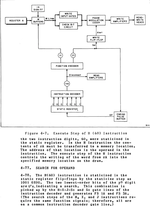
the location into which information is to be transferred. The least significant digits of instructions which do
not involve an operand or storage location are other than
o
or 5; therefore the two lowest-order bits of such in-structions are not 00, but 01 or 10. Table 4-3 shows the characteristic code, of instructions requiring a search-for-operand step.4-62. LOCATING THE OPERAND. The search process required to locate an operand in memory is identical to the search-for-instruction process.- Control of the operand search, however, differs from control of t~e instruction s~arch.
Figure 4-1 is also a block diagram of the
search-for-operand step. Differences between the instruction search and operand search in the figure are indicated by the notes. In locating an instruction, the c address in rC is compared with the timing band addresses; in locating an operand, the m address in rC is compared with the timing band addresses.
4-63. Although FS 63 alerts both the m-address output gates and the c-address output gates of rCt the CT FF determines which address is to be read out and compared. When an instruction is statici~ed. the output of STR FF2 determines whether an operand is necessary. Table 4-3 shows that the STR2 position of the staticized instruc-tion is always 0 when a search for operand is required.
-4-64. The STR2 output of the static register is sampled by gate 12 of the CT FF ~ure A-12) at tlOB of the staticize step. If the STR2 signal is low, indicating that a search must be made for the m address. the gate is permissive. When gate 12 is permissive the CT FF is set to CT, which controls readout of the m address from rC. When gate 12 is ~ocked by high signal STR2, the CT FF is restored to CT, which controls readout of the c address. The staticized instruction, however. has generated new fun£1ion signals for executing the instruc-tion so that the CT signal has no effect on rC until after the execution step.
4-65. The CT output of the CT FF is available at the m-address output gates of rC at t08. The LSD of the m
address. pSt goes from rC to the S buffers and the S lines and is available at the quinary and binary equality gates of the comparator (figure A-12) at tiB. The comparison and memory selection processes for the search-for-operand step are the same as those of the search-for-instruction step, (paragraph 4-5).
--~
4-66. The H, X, and J transfer instructions require a search-for-operand stept but the operand is a memory
location into which information must be written. Because these three instructions entail writing in the memory,
time must be allowed for the write circuits to be prepared. For this reason, the H, X. and J instructions generate
FS 3 for use in the search operation in addition to the normal search (Sc) function signals. Function signal 3
alerts gate B of STR FFI to sample the TS signal at t58. (In normal search. the T5 signal is sampled three pulse times later, at t8B.) Sampling at t58 allows the write circuits to prepare for writing by the time the execute step begins. If the T5 signal is low at t58, the STR FFI is set to a I, initiating the execute step of the instruc-tion stored in the static register.
4-67. E~ECUTE-INSTRUCTION STEP
4-68. The execute-instruction step is initiated when the seven bits of the two instruction digits are staticized in tbe static register and either of the two lowest-order bits of the p9 digit is a 1 (search-for-operand step is unnecessary), or when the search for-operand step has been completed and the STR FFI has been stepped to a 1 output. In both cases the combination of bits stored in the STR represents a specific instruction and can be decoded by the instruction decoder. The combination in the static register goes to the instruction decoder and function encoder to generate one or more function signals which execute the staticized instruction.
4-69. The Analysis of UCT Instructions manual lists the function signals generated for each instruction and the purpose of each of these signals. Sections 4-74 through 4-199, and the input-output manuals explain the details of the execution steps of typical instructions. The instructions not covered in detail in these sections and the input-output manuals are treated in functional block diagram form in Section V.
4-70. TWO-EXECUTION-STEP INSTRUCTIONS. Many instructions involve two execution steps. The add instruction (70), for example, adds two quantities in the first execution step and complements if necessary the sum of the addition in the second execution step. The function sign~ls
generated for the first step (AI) of the add instruction include FS 64. At tl08 of the Al step FS 64 at the
Flip-flop 1 bad been previously set to a 1 to accomplish the Al step. Setting FF2 to a 1 output sets up the com-bination in the static register for step A2; as a result,
a new set of function signals is generated to control the A2 step. The stepping gate similarly controls FFI and FF2 during many other instructions.
4-71. Table 4-3 shows the code combinations for the
steps of all UCT instructions. The table is divided into instructions which require only one execution step and those which require more than one. It is subdivided further into instructions which require a search-for-operand step and those w~ich do not. The third column, STH code. lists the code combinations for each step of each instruction after it has been staticized in the static register. The code positions marked by X are bits which are unnecessary to the staticize step. The X in the LSD - STR3 position is included only to balance each combination with the eight bits of the biquinary code.
4-72. TIMING OF THE BASIC OPERATION CYCLE
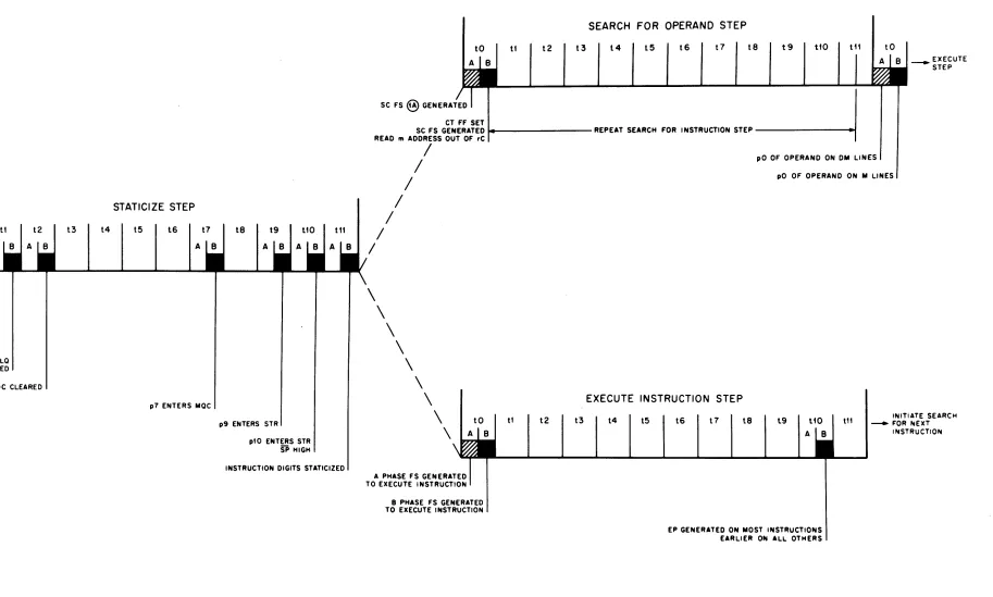
4-730 The four steps of the basic operation cycle
re-quire a minimum of four word times to complete. In-structions requiring no search-for-operand step~ take only three word times. Instructions with more than one execution step require more than four word times. The timing of the basic operation cycle with and
with-out a search for operand step is shown in figure 4-6. The timing of the various operations of the
for-operand step is identical to that of the search-for-instruction step. Therefore the sea~ch-for
operand step shows only the timing of operations unique to it. Although many other operations occur during each word time~ only the ones necessary to ex-plain the timing of the whole cycle are included. 4-74. PROCESSING A TYPICAL INSTRUCTION
4-75. This section applies the previously discussed details of the basic operation cycle to the proces-sing of an actual instruction. In the ~earch-for
instruction step. the operation of the memory read circuits was explained. Use of the H(60) instruction in this section permits explanation of the memory write circuits because the instruction requires a transfer of information in a register to a storage locationo
SEARCH FOR INSTRUCTION STEP
STR CLEARED TO ZEROS
SC FS @ GENERATED TS FF SET SC FS GENERATED pt LEAIIES rC
p1 ON M AND S LINES
p2 ON M AND S LINES
p3 ON M AND S LINES p4 ON CLINES
BAND CHANNEL AND QUADRANT SELECTED
SELECT NORMAL MEMORY SWITCH SELECT FAST MEMORY SWITCH SAMPLE TS WHEN WRITING
t6 t7 t8
A
pO OF INSTRUCTION ON OM LINES SZ FS @ GENERATED
SZ FS GENERATED pO OF INSTRUCTION WORD ENTERS rC
CLQ GENERATED
t3 t4
MaC CLEARED
READ FF SET
SAMPLE TS WHEN READING
STEP STR FF1 TO I INITIATE STATICIZE STEP
Figure 4-6.
STATICIZE STEP
t5 16
A
p7 ENTERS MaC
p9 ENTERS STR
p10 ENTERS STR
SP HIGH
INSTRUCTION DIGITS STATICIZED
SEARCH FOR OPERAND
tt t2 t3 l4 t5 t6
CT FF SET
SC FS GENERATED .... - - - REPEAT SEARCH FOR I NSTRUC" READ m ADDRESS OUT OF rC
/
/
/
\
\
\
/
\
/
/
/
\
\
\
\
\
A PHASE FS GENERATED TO EXECUTE INSTRUCTION
B PHASE FS GENERATED TO EXECUTE INSTRUCTION
EXECUTE INSTRUCTION
t I t2 t3 14 t5 t6 t'
EP GENERAl
[image:27.1225.270.1217.125.666.2]R INSTRUCTION STEP
t6 t7 t8
pO OF INSTRUCTION ON OM LINES S2 FS @ GENERATED
S2 FS GENERATED pO OF INSTRUCTION WORD ENTERS ,C
CLO GENERATED
t3 t4
MaC CLEARED
ITCH ITCH TlNG
READ FF SET
SAMPLE TS WHEN READING
STEP STR HI TO I
INITIATE STATICllE STEP
Figure 4-6.
STATICIZE STEP
t5 t6
p1 ENTERS MaC
p9 ENTERS STR
piO ENTERS STR
SP HIGH INSTRUCTION DIGITS STATICIZEO
SEARCH FOR OPERAND STEP
tl t2 t3 14 t5 t6 t7
CT FF SET
t8 t9 ttD t11
_ EXECUTE STEP
SC FS GENERATED .... - - - REPEAT SEARCH FOR INSTRUCTION STEP ---~
READ m ADDRESS OUT OF rC
/
/
\
\
/
/
\
\
/
/
/
\
\
\
\
\
B PHASE FS GENERATED TO EXECUTE INSTRUCTION
tt t2 t3
pO OF OPERAND ON OM LINES
pO OF OPERAND ON M LINES
EXECUTE INSTRUCTION STEP
t4 t5 t6 t7 t8 t9
EP GENERATED ON MOST INSTRUCTIONS EARLIER ON ALL OTHERS
til - FOR NEXT INITiATE SEARCH
INSTRuCTION
Timing of Basic Operation Cycle
3110
[image:28.1224.258.1171.91.640.2]Table 4-3. Instruction Code Combinations
INS'mUCTIOl'S WITH ONE EXECUm STEP (SEARCH)
,-Instruction Biquinary
sm
Code StepsS 5 5 5 5 5 5 T T T T T T T R R R R R R R 8 7 6 5 4 2 1
05 (Y): (m) ~ rX
o
0 0 0 100 0 XXXX X X 0 0 <Sc 00).0000 I X 0 1 (y 06)
20 (P): Superimpose (m) and
o 0 1 0
o 0 0 0
X X X X X X 0 0 (Sc 00) (rA)- >
rAo X 1 0
o
X 0 1 (P 21)25 (8): (m)
->rA
o
0 1 0 1 000 X X X X X X 0 0 (Sc 00)o
X 1 ,0 1 X 0 1 (B 26)30 (L): (m)
- >
rL 001 1o
0 0 0 X X X X X X 0 0 (Sc 00)o XII
o
X 0 I (L 31)35 <E): Logically multiply 001 I 1 000 X X X X X X 0 0 (Sc 00) (m) and (rA)
--->
rAo
XII 1 X 0 1 (E 36) 50 (J): (rL)- >
m 1 000 000 0 1 000o X 0 0
(J-Sc 50)1 000
o
X 0 1 (J-Ex 51)60 (H): (rA)
--->
m 100 1o
0 0 0 1 X 0 1 X X 0 0 (H-Sc 60)1 X 0 1
o
X 0 1 (H-Ex 61) [image:29.620.57.582.66.747.2]INSlliUCTIONS WITH
ONE.
EXECUTE pTEP ( NO SEARCH)I ns true tion Biquinary S'IR Code Steps
S S S S S S S T T T T T T T
R R R R
R R R 876 5 4 2 112 (G): RR --:>UCT 000 1 001 0
o
X 0 1o
X 1 0 (G 12)(rA)
+
(rX) ->rA17 (R): OCT ->RR 000 1 101 0
o
X 0 1 1 X 1 0 (R 17 )(rA) - > r A
+
rX47 (Z2): Select output
o
1 0 0 101 0o
1 0 0 1 X 1 0 (Z2 47) stacker offast reader
67 Stop 100 1 101 0 1 X 0 1 1 X 1 0 (Stop 67)
72 (CC>: Feed one card 1 0 1 0 001 0 1 X 1 0
o
X 1 0 (CC 72) fast reader77 (K): (rA) - > r L 101 0 101 0 1 X 1 0 1 X 1 0 (K 77)
82 (Q): (rA) : (rL) 101 1
o
0 1 0 1 X 1 0o
X 1 0 (Q 62)If (rA)
=
(rL). go to mIf (rA)
+
(rL). go to c87 (T): erA) : (rL) 101 1 101 0 1 XII 1 X 1 0 (T 87)
If (rA)
>
(rL), go to mIf
(rA) ~ (rL), go to c" . . .
INSTRUCTIONS WITH TWO OR MORE EXECUTE StEPS (SEARCH)
Instruction Biquinary SIR Code :steps
5 5 S 5 S 5 S
TTTT T T T R R R R R R R
8 7 6 5 4 2 1
55 (D): (m) f (rL) --->rA 100 0 1 000 X X X X X X 0 0 (Sc 00)
remainder --->rX 1 000 1 X 0 1 (Dl 56)
1 000 1 X 1 1 (D2 58)
100 1 1 XII (D3 68)
70 (A): (m)
+
(rA) ->rA 101 0o
0 0 0XXXX
X X 0 0 <Sc 00)1 X 1 0 X X 0 1 (AI 71)
1 X 1 0 X XlI (A2 73)
75 (5):
(rA) - (m) --->rA
101 0 100 0 X X X X X X 0 0 (5c 00)1 X 1 0 X X 0 1 (51 76)
1 X 1 0 X XII (52 78)
85 (M): (m) x
(rL) --->rA+rX
101 1 1 000 X X X X X X 0 0 <Sc 00)1 X 1 1 1
X
0 1 (Ml 86)I~TRUCTIOr-s WITH
nvo
OR MORE EXECUTE STEPS (NO SEARCH)Instruction Biquinary
sm
Code StepsS S S S S S S TTTT T T T
R R R R R R R 8 7 6 5 4 2 1
II (PRl): memory --->print buffer 000 1 000 1
o
X 0 I X X 0 1 (PRI 11)o
X 0 I X XII (PR2 13)16 (PFI): paper advance 000 1 100 1
o
X 0 1 X X 0 1 (PFI 16)o
X 0 1 X XII (PF2 18)22
(Ill): Test read punch unito
0 1 0 001 0o
X 1 0o
X 1 0 (Ill 22) card bufferIf loaded. go to m
o
X 1 0 X XII (112 23)If not loaded, go to c
21 (121): If printing or paper 001 0 101 0
o
X 1 0 1 X 1 0 (121 27) feeding, go to cIf not printing or
o
X 1 0 X XII (112 28) paper feeding, go to m;(re)
- >
rA32 (N): Right circular shift 001 1 001 0
o
XII X X 1 0 (Nl 32) IrAI ->rX;,rXI
->rA n placeso
X I Io
X I I (N2 33)31 (V): Left shift rA n places
o
0 I 1 1 0 1 0o
X 1 1 X X I 0 (VI 31) Lose ff5DReplace LSD with 0
o
X I 1 I X I 1 (V2 38)42 (131): Test card buffer fast
o
1 0 0 001 0o
I 0 0o
X I 0 (131 42)reader
If loaded. go to m
o
X I 0 X X I I (112 23)If not loaded. go to c
INSlRUCTIONS WITH nvo OR MORE EXECUm STEPS (NO SEARCH) (cont)
Ins truction Biquinary STR Code Steps
S 5 S S S S
s
r
T T T T TTR R R R R R R 8 7 6 5 4 2 1
46 (Wll):Read punch unit
o
1 0 0 100 1o
1 0 0 I X 0 1 (WIl 46)card buffer
->
main memory
o
1 0 0 1 X I 1 (W12 48)62 (ZSI): Zero suppress 100 1 001 0 1 X 0 1
o
X 1 0 <ZS1 62) Rem Rand wordin rA 1 X 0 1
o
XII (ZS2 63)61 (W21): Start read punch unit 101 1 000 1 1 X 1 1
o
X 0 1 (W21 81)and main memory
--->
1 X 1 1o
XII (W22 83)Read punch unit card buffer
96 (W31): Fast reader card 1 100 100 1 1 1 0 0 1 X 0 1 (W31 96)
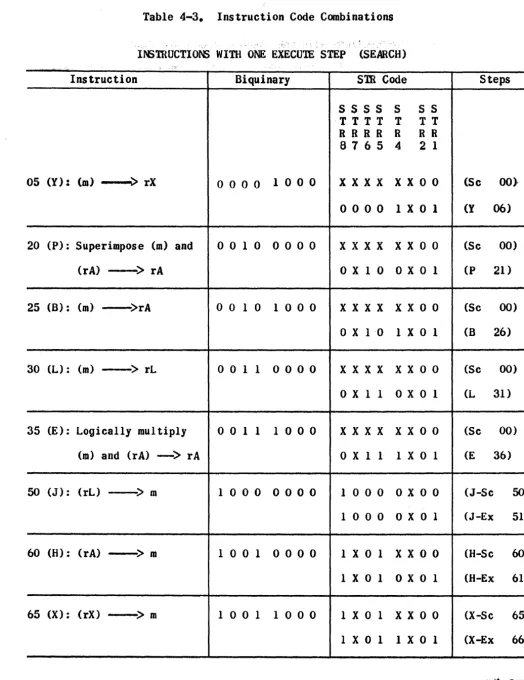
REGISTER A
WRITE INPUT GATES
CHECK BIT CIRCUIT
Disconnect
PHASE MODULATION
CODER
Alert
READ AMPLIFIERS
EP
WRITE AMPLIFIERS
ENDING PULSE BUFFER
Figure 4-7. Execute Step of'H (60) Instruction the two instruction digits, 60, were staticized in the static registero In the H instruction the con-tents of rA must be transferred to a memory location. The address of that location is the operand in the
instructiono The execute step of the H instruction
controls the writing of the word from rA into the specified memory location on the drum.
4-77. SEARCH FOR OPERAND
4-78. The H(60) instruction is staticized in the static register flip-flops by the staticize step as 1001 OXOO. The two lowest-order bits of the p9 digit are O's. indicating a search. This combination is
picked up by the H-X-J-Sc and Sc gate lines of the instruction decoder and generates FS IA and FS 3A. (The search steps of the Ht X~ and J instructions re-quire the same function signals; therefore. all are on a common instruction decoder gate line.)
4-32
READ-WRITE HEADS
[image:34.617.41.547.57.751.2]4-790 Function signal lA generates FS 58+. FS 74,
FS 63 and FS 10 Function signal 58+ blocks readout from rA onto the S lineso Function signal 74 sets the CP FF to produce a CP signalo Function signal 63, in conjunction with the CT signal. causes readout of the m address from rC onto the S lines. Function sig-nal 1 alerts the input gates of the M buffer to enable the timing band signals from the drum to enter the M lines.
4-80. The 1001 OXOO STR output combination also gen-erates FS 3A (H-X-J 56 gate) which gengen-erates F5 3 to alert the STR FFI stepping gate. At t5B of the search-for-operand stept the output of the TS FF is sampled by gate B of FFI. A low TS signal and F5 3 make gate 8 permissive and step FFI from a 0 output to a 1 output. The new STR output combination of 1001 OXOI (61) is
present at the instruction decoder at t68.
4-81. At t68. F5 3 sets the write FF (figure A-19)
at gate 58 to prepare the write circuits for the execute step of the instruction.
4-82. When gate 8 of STR FFI is permissive at t6A, a high RCT2 signal is generated which goes to the input gates of the CT FF and to buffer 104 of the write cir-cuits. The hiAh RCT2 sign,l restores the CT FF~ gener-ating the low CT signal which controls readout of the c address from rC and generates the write pedestal (paragraph 6-243). The new STR combination causes the function signals for search to end at t7A. The search-for-operand step has located the operand. which is the storage location designated by the m address.
4-83. EXECUTE THE H(60) INSTRUCTION
4-86. Function signal 11 alerts input gates 7A. 7B,
7et and 7D of the M buffers (figure A-6). These gates
are permissive to the four bits of the pO digit (AIM,
A2M,
A3M,
and A4M) fromrA at t7B.
and the contents of rA enters onto the M lines. Gate 6 of the M buffers. also alerted by FS I I , also is permissive at t16 to a low A-"signal. This condition indicates that the sign of the contents of rAt which has been stored in the rA sign flip-flop, is minus. If the sign of rA is plus. low A- is absent from g~te 06. The sign position of the word (t78) on theAIM
lines contains0,
indicating a plus sign. The word-and its sign are sent from rA onto theM
lines and into the write circuits (figures A-19 and A-20).4-87. At t4B of the execute step FS 21 operates gate 19 of ~he static register to generate the EP and Reset-TS signals. Because the
H
tX
t and J instructionsin-volve writing on the drum and therefore ~e~uire less time for execution than most instructions. the EP
signal is generated early. The function signals for the instruction are lost at t7B. Th~ TS Fr is restored so that the set output of the flip-flop9 TS~ cannot set the read flip-flop. Normally, at t8B, the ~ad
flip-flop (figure A-19) is set by FS I, TS and OF. All these signals will be present at t8B because the function signals for search. will be available at t16. To keep the read flip-flop restored until reading is required. the Reset-TS signal restores the TS FF, keep-ing the TS signal high. High TS blocks gate 42A of the read flip-flop, keeping it restored. The zero combination in the STR initiates a search for the next instruction.
4-88. MEMORY WRITE OPERATION
4-89. During a write operation, information and check bits are sent on the M lines to the "phase-modulation coder where ea~h input signal is coded into a phase~
modulated pulse representation for memory recording. The resulting pulse is amplified in the write amplifier and drives the write heads.
4-900 At t7A, FS IIA electronically disconnects the read amplifiers from the write circuits by generating the write pedestal (paragraph 6-243). Control signal RCT2, present for only one pulse time. has generated
the write pedestal from t6A until t7A. For writing on the fast-access bands the IR output of the
write-pedestal generator disconnects the read amplifiers of the fast-access heads.
4-91. The bits of each digit to be written are sent in parallel to the check-bit circuit and to the write input circuits. The check-bit circuit is explained in paragraph 4-202: Each of the four bits of the digit to be written is delayed a pulse time by two comple-menting amplifiers before going to the input gates of the phase-modulation coder, so that the check bit9 . and the information bits can be written
simultaneous-ly. Computing the check bit requires a full pulse time. At t9B the information bits and a check bit are present
at the input gates to the phase-modulation coder. The write flip-flop output alerts the input gates at t8B and for a full word time thereafter. The operation of the phase-modulation coder is explained in paragraphs
3-208 through 3~212. The bits are converted into a phase-modulated waveshape which goes directly to the read-write heads and is written on the drum in the location specified by the m address.
4-92. ARITHMETIC OPERATIONS
4-93. ADDITION ANQ SUBTRACTION
4-94. ADD INSTRUCTION. The functions of the add in-struction are: add algebraically the quantity in- the storage location designated by m ~o the contents of rA. store the result in rAt compute the sign of the sum and store the sign in the rA sign flip-flop. The quantity in the memory is the addend; the quantity in rA is the augend.
4-95. Before addition takes place:
(1) The search for the instruction has been completed.
(2) The add instruction (70) has been staticized. (3) The staticized instruction has initiated a
search for the operand (m address). which in this instruction is the addend.
(4) The augend has been stored in rA by a pre-vious instruction and its sign has been stored in the register A sign flip-flop. The add instruction re~uires two execution steps. Al and A2.
4-96. A-I STEP. In the first step of addition, AI, (figure 4-8a), the signs of the augend and addend are compared at the input gates
of
the CP FF. The gates det'ermine from thetwo signs whether the~ugend is to be complemented (CP) or not complemented <CP) before addition. This infor-mation controls the complementing circuit of the quin-ary adder. The sign of the augend is compared with the
CP
output of the complement flip-flop at the input gates of the rA sign flip-flop to determine the sign of the sum. Once determined, the sign of the sum is stored in the rA sign -flip-flop. The augend in rA is sent on the S lines into the binary and quinary adders. The addend from the memory location designated by the m address is sent on the M lines into the binary andQuinary adders. The adders add the two quantities digit by digit and transfer the sum on the' 0 lines into rAe
4-97. The staticized digits of the Al step (71) gen-erate function signals 4~ 50. 55+. 64, and 15 at taB to execute the Al step. Function signal 4 alerts the
input gates of the complement (CP) FF. Gates 8 and 9 of the CP FF (paragraph 3-138) operate during the add instruction to sample the signs of the two quantities. If the signs are unlike. one of the gates operates to set the CP FF to CPT which will cause the augend digits to be complemented. If the signs are alike, gates 8 ~d 9 are blocked. the flip-flop remains restored to
CPt and the augend is not complemented.
4-98. Function signal 55+ blocks the recirculation gates of rA. and the digits of the augend go to the S buffers and the 5 lines. Function signal 50 alerts the quinary and binary adders gates at tOB.
4-99. The quinary bits of the pi digit of the addend (MI. M2. and M3) go to the input gates of the decimal carry adder (figure A-II) and the quinary carry gates (figure A-12). The input gates of the decimal carry adder sample the A and C signals from the binary and quinary circuits to determine whether a carry bit is to
be added to the two digits being added. Because the pI
digits aIe th~ first to be added there can be no carry, and the A or C signal. or both. will be low. The out-puts of the decimal carry adder go to the quinary adder. They represent the quinary bits of each digit of the addend.
4-100. The quinary bits of the pI digit of the augend (51. 52, and 53) go to the input gates of the comple-menting circuit (figure A-II). If the CP (complement)
signal alerts the gates, the eircui.;L.produces the com-plement of the input bits. If the CP (no complement) signal alerts the gates, the quinary S bits pass
through the circuit unchanged.
4-101. The quinary S bits and M bits also are sent in parallel to the quinary carry circuit. Any combination-of quinary bits which indicates the need for quinary carry generates C and C' signals from the quinary carry circuit. The gates are blocked by combinatio~s which require no quinary carry, generating the low C signal. The low C signal, if generated, is used in conjunction with the
A
signal to indicate a decimal carry intothe addition of the next two digfts. The low C' sig-nal indicates the presence of quinary ca~ry and causes a carry bit to be added in the addition of the binary bits in the binary adder.
4-102. The quinary outputs of the decimal carry ad-der and those of the complementing circuit are added in the quinary adder gates. One or two of the adder gates is permissive to the input corebinationst
pro-ducing a high 0 output signal. A high 0 output signal
indicates a 1 bit. a low 0 output signal indicates a Obit.
4-103. The bi~ary bits of the two quanii~ies are added in t~e binary adder (figure A-12) at the same time as the quinary bits. Initially, the M4 and 54 bin a r y bit s are' com par ~ i nth e bin a rye qua 1 i t Y gat e s • The gates. alerted by CPt sample the two binary bits during a normal addition. If either bit is a 1. a signal indicating the 1 bit goes to the binary carry circuit to generate a binary carry signal
At
which will be used with the C signal, if present. in theaddition of the next two digits. The carry circuit also
send~ the At signal to gate 6 of the binary adder.
It
the C signal is low. gate 6 is permissive to theA'
signal and the 042 output is high, indicating a 1 bit in the M5B of the su~ digit. No decimal carry will beg e n era ted i f the C s i 9 n _ al i s low._-
105. If the M4 and the S4 bits each has a value of O. the binaIY equ~litY gates are blocked. generating low
sign~ls A and A' which indicate no binary carry. The low A' signal goes to gate 7 of the binary adder which is permissive only if quinary carry is present. a con-dition indicated by the low C' signal. If the gate is permissive. the 041 o~tput is hight indicating a" 1 in
the MSB position of the sum digit. If quinary carry is absent. the C' signal is high blocking gate 7 and producing a low 041 bit. A low 041 output signal in-dicates a 0 in the MSB of the sum digit. The
Q
signal outputs of the quinary adder and the binary adder are sent to the sum input buffers of rAe The sum digits are stored in rA during the Al step.4-106.
If
the sum of two quantities with unlike signs is zero, the sign of that sum must be forced t