~~I
x)·
/0
I
JUt.
6 1983
DEVICE lEVEL DITERFACE
PRELIMINARY
.JUNE 1983
ABSTRACT:
FOREWORD
This interface was developed to specify a common interface definition and specify connector pin assignments and functional protocols. Physical
1.0
2.0
3.0
TABLE OF CONTENTS
PAGE
Scope ••••••••••••••••••••••••••••••••••••••••••••••••••••••• 1
1.1 Defin1t1ons ••••••••••••••••••••••••••••••••••••••••••• ~ • ••••••• 2
1.1.1 State Nomenclature ••••••••••••••••••••••••••••••••••••• 2 Physical Characteristlcs •••• ~ •••••••••••••••••••••••••••••••••••••••• 3
2.1 2.2 2.3 2.4
Cabling Configuration •••••••••••••••••••••••••••••••••••••••••• 3 Connector Specification •••••••••••••••••••••••••••••••••••••••• 3 Cable Characteristics •••••••••••••••••••••••••••••••••••••••••• 3 Electrical Characteristics ••••••••••••••••••••••••••••••••••••• 8
2.4.1
2.4.2
2.4.3
Bidirectional Control Bus Lines •••••••••••••••••••••••• 8
2.4.1.1 2.4.1.2 2.4.1.3
Control Bus Drivers •••••••••••••••••••••••••• 8 Control Bus Receivers •••••••••••••••••••••••• 8 Control Bus Termination ••••••••••••••••••••• 10
Single Ended Lines •••••••••••••••••••••••••••••••••••• l0
2.4.2.1 2.4.2.2 2.4.2.3 2.4.2.4
Single Ended Line Drivers ••••••••••••••••••• lO Single Ended Line Receivers ••••••••••••••••• l0 Single Ended Line Termination ••••••••••••••• 10 Port Enable Termination ••••••••••••••••••••• lO
Differenti~l Lines •••••••••••••••••••••••••••••••••••• l3
2.4.3.1 2.4.3.2 2.4.3.3
Differential Line Drivers ••••••••••••••••••• 13 Differential Line Receivers ••••••••••••••••• 13 Differential Line Termination ••••••••••••••• 13
Signal Definitions •••••••••••••••••••••••••••••••••••••••••••••••••• 16
3.1 Control Bus ••••••••••••••••••••••••••••••••••••••••••••••••••• 16
3.1.1
3.1.2
3.1.3
Radial Mode ••••••••••••••••••••••••••••••••••••••••••• 16
3.1.1.1 3.1.1.2
Select Out Mode ••••••••••••••••••••••••••••• 16 Attention In Mode ••••••••••••••••••••••••••• 16
Daisy ChainHOde •••••••••••••••••••••••••••••••••••••• 17
3.1.2.1 3.1.2.2 3.1.2.3
Command OUt ••••••••••••••••••••••••••••••••• l7
Parameter OUt ••••••••••••••••••••••••••••••• 17 Parameter In •••••••••••••••••••••••••••••••• 17
4.0
3.2
3.3
PAGE
Control Interface ••••••••••••••••••••••••••••••••••••••••••••• 18
3.2.1 3.2.2 3.2.3 3.2.4 3.2.5 3.2.6 3.2.7 3.2.8 3.2.9 3.2.10 3.2.11 3.2.12
Port Enable ••••••••• " •••••••••••••••••••••••••••••••••. 18
Bus Direction OUt ••••••••••••••••••••••••••••••••••••• 19 Select Out/Attention In Strobe •••••••••••••••••••••••• 19 3.2.3.1 Select Out Strobe ••••••••••••••••••••••••••• 19 3.2.3.2 Attention In Strobe ••••••••••••••••••••••••• 19
Command Request ••••••••••••••••••••••••••••••••••••••• 20
Parameter Request ••••••••••••••••••••••••••••••••••••• 20
Bus Acknowledge ••••••••••••••••••••••••••••••••••••••• 20 Busy •••••••••••••••••••••••••••••••••••••••••••••••••• 20 Attention ••••••••••••••••••••••••••••••••••••••••••••• 20 Index ••••••••••••••••••••••••••••••••••••••••••••••••• 21 Sector Mark ••••••••••••••••••••••••••••••••••••••••••• 21 Read Gate ••••••••••••••••••••••••••••••••••••••••••••• 21 Write Gate •••••••••••••••••••••••••••••••••••••••••••• 21
Read/Write Signals ••••••••••••••••••• ~ •••••••••••••••••••••••• 22
3.3.1 3.3.2 3.3.3 3.3.4
Read Data •••••••••••••••••••••••••• · ••••••••••••••••••• 22
Read/Reference Clock •••••••••••••••••••••••••••••••••• 22
Write Data •••••••••••••••••••••••••••••••••••••••••••• 22
Write Clock ••••••••••••••••••••••••••••••••••••••••••• 22
Command Structure ••••••••••••••••••••••••••••••••••••••••••••••••••• 23
4.1
4.2
Commands With Parameter Out ••••••••••••••••••••••••••••••••••• 27
4.1.1 4.1.2 4.1.3 4.1.4 4.1.5 4.1.6 4.1.7 4.1.8 4.1.9 4.1.10 4.1.11 4.1.12
Attention Control ••••••••••••••••••••••••••••••••••••• 27
Write Control ••••••••••••••••••••••••••••••••••••••••• 27
Set Upper Cylinder Address •••••••••••••••••••••••••••• 28 Set Lower Cylinder Address •••••••••••••••••••••••••••• 28 Select Moving Head •••••••••••••••••••••••••••••••••••• 28 Load Attribute Number ••••••••••••••••••••••••••••••••• 29 Load Device Attribute ••••••••••••••••••••••••••••••••• 29
Spin Control •••••••••••••••••••••••••••••••••••••••••• 29
Load Sector Pulses Per Track High •••••• ~ •••••••••••••• 29 Load Sector Pulses Per Track Medium ••••••••••••••••••• 30 Load Sector Pulses Per Track Low •••••••••••••••••••••• 30
Load Test Byte •••••••••••••••••••••••••••••••••••••••• 31
Commands with Parameter In •••••••••••••••••••••••••••••••••••• 31 4.2.1 4.2.2 4.2.3 4.2.4 4.2.5 4.2.6 4.2.7
Report tlIllegal Command" •••••••••••••••••••••••••••••• 3l Clear Fault ••• _ ••••••••••••••••••••••••••••••••••••••• • 31
Clear Attention ••••••••••••••••••••••••••••••••••••••• 31
Seek •••••••••••••••••••••••••••••••••••••••••••••••••• 31 Rezero •••••••••••••••••••••••••••••••••••••••••••••••• 32
4.2.8 4.2.9 4.2.10 4.2.11 4.2.12 4.2.13 4.2.14 4.2.15 PAGE
Report General Status Byte •••••••••••••••••••••••••••• 32 Report Device Attribute ••••••••••••••••••••••••••••••• 32 Set Attention ••••••••••••••••••••••••••••••••••••••••• 32 Selective Reset ••••••••••••••••••••••••••••••••••••••• 33 Partition Track ••••••••••••••••••••••••••••••••••••••• 33 Report Cylinder High •••••••••••••••••••••••••••.••••••• 33 Report Cylinder Low ••••••••••••••••••••••••••••••••••• 34 Report Test Byte •••••••••••••••••••••••••••••••••••••• 34
4.3 Device Attribute Commands ••••••••••••••••••••••••••••••••••••• 36
4.3.1 4.3.2 4.3.3 4.3.4 4.3.5 4.3.6 4.3.7 4.3.8 4.3.9 4.3.10 4.3.11 4.3.12 4.3.13 4.3.14 4.3.15 4.3.16 4.3.17 4.3.18 4.3.19 4.3.20 4.3.21 4.3.22 4.3.23 4.3.24 4.3.25 4.3.26 4.3.27 4.3.28 4.3.29 4.3.30 4.3.31 4.3.32 4.3.33 4.3.34 4.3.35 4.3.36
User ID ••••••••••••••••••••••••••••••••••••••••••••••• 36
Model 1D High ••••••••••••••••••••••••••••••••••••••••• 36 Model ID Low •••••••••••••••••••••••••••••••••••••••••• 36
Revision ID ••••••••••••••••••••••••••••••••••••••••••• 37
Device Type ID •••••••••••••••••••••••••••••••••••••••• 37
Attribute Table Modification •••••••••••••••••••••••••• 37
Table ID •••••••••••••••••••••••••••••••••••••••••••••• 38
Bytes Per Track Bigh •••••••••••••••••••••••••••••••••• 38 Bytes Per Track Medium •••••••• ~ •••••••• ~ •••••••••••••• 38 Bytes Per Track Low ••••••••••••••••••••••••••••••••••• 38 Bytes Per Sector High ••••••••••••••••••••••••••••••••• 39 Bytes Per Sector Medium ••••••••••••••••••••••••••••••• 39 Bytes Per Sector Low •••••••••••••••••••••••••••••••••• 39 Sector Pulses Per Track High •••••••••••••••••••••••••• 39 Sector Pulses Per Track Medium •••••••••••••••••••••••• 39 Sector Pulses Per Track Low ••••••••••••••••••••••••••• 39 Sectoring Method •••••••••••••••••••••••••••••••••••••• 40 Number of Cylinders Low ••••••••••••••••••••••••••••••• 40 Number of Cylinders Low ••••••••••••••••••••••••••••••• 40 Number of Moving Heads •••••••••••••••••••••••••••••••• 40 Header Encoding Method #1 ••••••••••••••••••••••••••••• 41 Preamble #1 Length •••••••••••••••••••••••••••••••••••• 41 Preamble #1 Pattern ••••••••••••••••••••••••••••••••••• 41 Synchronization II Pattern •••••••••••••••••••••••••••• 41 Postamble '1 Leng.th ••••••••••••••••••••••••••••••••••• 42 Post amble #1 Pattern •••••••••••••••••••••••••••••••••• 42 Gap #1 Length ••••••••••••••••••••••••••••••••••••••••• 42
Gap II Patteru •••••••••••••••••••••••••••••••••••••••• 42
Data Encoding Method #2 ••••••••••••••••••••••••••••••• 42 Preamble #2 Length •••••••••••••••••••••••••••••••••••• 42 Preamble #2 Pattern ••••••••••••••••••••••••••••••••••• 42 Synchronization '2 Pattern •••••••••••••••••••••••••••• 43 Postamble #2 Length ••••••••••••••••••••••••••••••••••• 43 Postamble #2 Pattern •••••••••••••••••••••••••••••••••• 43 Gap #2 Length ••••••••••••••••••••••••••••••••••••••••• 43 Gap '2 Pattern •••••••••••••••••••••••••••••••••••••••• 43 4.4 Status Reporting •••••••••••••••••••••••••••••••••••••••••••••• 46
[image:5.620.64.544.82.792.2]4.4.2 4.4.3 4.4.1.1 4.4.1.2 4.4.1.3 4.4.1.4 4.4.1.5 4.4.1.6 4.4.1.7 4.4.1.8
Bit 0 Bit 1 Bit 2 Bit 3 Bit 4 Bit 5 Bit 6 Bit 7
PAGE Not Ready ••••••••••••••••••••••••••• 46 Control Bus Error ••••••••••••••••••• 46 Illegal Command ••••••••••••••••••••• 46 Illegal Parameter ••••••••••••••••••• 47 Sense Byte 1 •••••••••••••••••••••••• 47 Sense Byte 2 ••••••••••••••••• ~ •••••• 47 Busy Executing •••••••••••••••••••••• 47 Normal Comp1ete ••••••••••••••••••••• 47
Sense Byte 1 ••• , •••••••••••••••••••••••••••••••••••••• 48
4.4.2.1 4.4.2.2 4.4.2.3 4.4.2.4 4.4.2.5
Bit 0 Bit 1
Bit 2 Bit 4 Bit 5
Seek Error •••••••••••••••••••••••••• 48 Read/Write Fau1t •••••••••••••••••••• 48 Power Fau1t ••••••••••••••••••••••••• 48 Speed Error ••••••••••••••••••••••••• 49 Command Reject •••••••••••••••••••••• 49
Sense Byte 2 •••••••••••••••••••••••••••••••••••••••••• 49
4.4.3.1 4.4.3.2 4.4.3.3 4.4.3.4
Bit 0 Bit 1 Bit 5 Bit 6
Initial State ••••••••• ~ ••••••••••••• 49 Ready Transition •••••••••••••••••••• 49 Device Attribute Table Modified ••••• 50 Positioned Within Write ••••••••••••• 50 Protected Area
5.0 Timing Specification •••••••••••••••••••••••••••••••••••••••••••••••• 51
5.1 Control Bus Timing •••••••••••••••••••••••••••••••••••••••••••• 51
5.1.1 5.1.2 5.1.3
Selection Timing •••••••••••••••••••••••••••••••••••••• 51 Attention Timing •••••••••••••••••••••••••••••••••••••• 51 Control Bus Handshake Timing •••••••••••••••••••••••••• 52
5.2 Index and Sector Timing ••••••••••••••••••••••••••••••••••••••• 52 5.3 Reference Clock Timing •••••••••••••••••••••••••••••••••••••••• 52
5.4 Read Timing ••••••••••••••••••••••••••••••••••••••••••••••••••• 52 5.5 Write Timing •••••••••••••••••••••••••••••••••••••••••••••••••• 52
5.6 Data Format and Data Control Timing ••••••••••••••••••••••••••• 53
5.6.1
5.6.2
5.6.35.6.4
5.6.5
5.6.6
5.6.7
Read Initialization Time •••••••••••••••••••••••••••••• 53 Write-to-Read Recovery Time ••••••••••••••••••••••••••• 53 Read-To-Write Recovery Time ••••••••••••••••••••••••••• 53 Read PLO Synchron!zation •••••••••••••••••••••••••••••• 53
Sync Pattern •••••••••••••• • " •••••••••••••••••••••••••• ·.53
Write Driver Turn On •••••••••••••••••••••••••••••••••• 53 Gap 2 Tolerance ••••••••••••••••••••••••••••••••••••••• 53
5.7 Control Timing ... 53
1-1
2-1
2-2
2-3
4-1
':-'2
4-3 4-4
4-5 4-6
TABLES
PAGE
St·ate Nomenclature •••••••••••••••••••••••••••••••••••••••••• · •••••••• 2
Dimensions of Interface Cable Plug •••••••••••••••••••••••••••••••••• 5
Dimensions of Interface Cabl'e Receptacle •••••••••••••••••••••••••••• 5
Pin Assignment •••••••••••••••••••••••••••••••••••••••••••• ••••••••• 15
Commands With Parameter Out •••••••••••••••••••••••••••••••••••••••• 25
CO!ll!!lsnds With Parameter In ••••••••••••••••••••••••••••••••••••••••• 26
Device Attributes •••••••••••••••••••••••••••••••••••••••••••••••••• 35
General Status Byte •••••••••••••••••••••••••••• ~ •••• ~ •••••••••••••• 44
Sense Byte 1 ••••••••••••••••••••••••••••••••••••••••••••••••••••••• 45
FIGURES
PAGE
2-1 Interface Configuration ••••••••••••••••••••••••••••••••••••••••••••• 4
Interface Cable Plug •••••••••••••••••••••••••••••••••••••••• ~ ••••••• 6 2-3 Interface Cable Receptacle •••••••••••••••••••••••••••••••••••••••••• 7
2-4 Cable Configuration for
Bidirectional Control Bus Signals ••••••••••••••••••••••••••••••••• 9
2-5 Cable Configuration for Unidirectional Signal
Ended Lines from Host •••••••••••••••••••••••••••••••••••••••••••• 1l
2-6 Cable Configuration for Port Enable •••••••••••••••••••••••••••••••• 11
2-7 Cable Configuration for Unidirectional Signal
Ended Lines from Devices ••••••••••••••••••.••••••••••••••••••••••• l2
2-8 Cable Configuration for Differential Lines From Host ••••••••••••••• l4
2-9 Cable Configuration for Differential Lines from Device ••••••••••••• 14
4-1 Sector Formats for Attributes Hex 30-47 •••••••••••••••••••••••••••• 41
5-1 Select Timing •••••••••••••••••••••••••••••••••••••••••••••••••••••• 55
5-2 Attention Timing ••••••••••••••••••••••••••••••••••••••••••••••••••• 56
5-3 Command/Parameter Out Sequence ••••••••••••••••••••••••••••••••••••• 57
5-4 Command/Parameter In Sequence •••••••••••••••••••••••••••••••••••••• 58
5-5 Index/Sector Timing •••••••••••••••••••••••••••••••••••••••••••••••• 59
Reference Clock Timing ••••••••••••••••••••••••••••••••••••••••••••• 60
~7 Read Timing •••••••••••••••••••••••••••••••••••••••••••••••••••••••• 61
1.0 Scope
This standard applies to fixed disk drive(s) and defines the necessary functional and electrical requirements (including logic signals) and the mechanical requirements of the interface for connection of conforming fixed disk drive(s) to host system(s). This standard is distinct from a specification in that it delineates a minimum set of requirements
consistent with compatibility and interchangeability at the interface level.
This standard will facilitate the interconnection of rigid disk drive(s) to host system(s) by a user that has available the technical capabilities to verify and test performance up through the functional level. The user should have the capability to specify the overall system hardware and software that will be unique for a particular device and host
combination.
This standard by itself does not guarantee plug compatibility of devices meeting this standard. To obtain total interchangeability of devices an operational specification must be defined. Neither the operating
specification nor the power requirements are defined by this standard.
This standard does not prescribe the magnetic encoding or decoding method, the recording techniques, nor the format used to write or read data but allows the reporting of all of the above. Unique
characteristics offered by a vendor are allowed.
The design of this interface provides the following features:
1. Addressability of up to 8 devices.
2. Transfer data across the interface via a close loop clocked NRZ format
3. Daisy chain configuration utilizing a 50 wire flat ribbon cable.
4. Supports a radial attention and selection capability throught the daisy chain bus.
5. Permits self configuration of the system and self definition of the individual devices.
1.1 Definitions
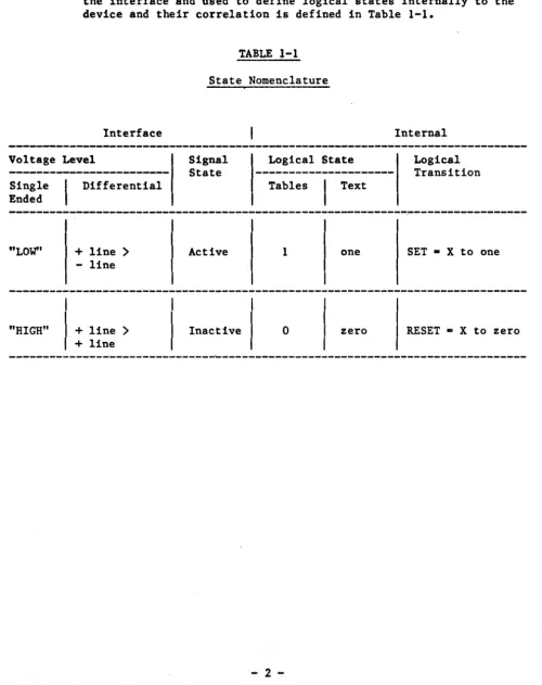
1.1.1 State Nomenclature
The nomenclature used to define voltage levels and signal states on the interface and used to define logical states internally to the device and their correlation is defined in Table 1-1.
TABLE 1-1
State Nomenclature
Interface Internal
Voltage Level Signal Logical State Logical
--- State Single
Ended
"LOW"
"HIGH"
Differential
+
line>
- line+
line>
+
lineActive
Inactive
--- Transition
Tables Text
1 one SET - X to one
o
zero RESET - X to zero [image:10.620.58.559.135.767.2]---~---~---2.0 Physical Characteristics
Unless otherwise indicated, all values are specified with a plus or minus five percent tolerance.
2.1 Cabling Configuration
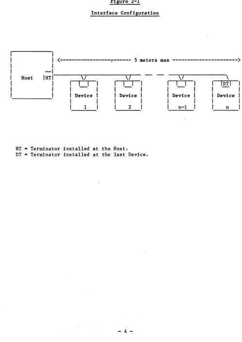
The device shall be connected to a host by means of a 50 conductor flat ribbon or equivalent cable. Five meters (5 m) shall be the maxim~ length of the interface cable. Note that the cumulative length of the eable in a daisy ehain string shall not exceed five meters. See Figure 2-1.
Delivery of primary power (AC and/or DC) shall not be accomplished on the interface cable. A separate DC common (ground) may be provided. Specifications for power supply cabling and grounding requirements are not a subject of this standard. Refer to vendor specifications for power/ground information.
2.2 Connector Specification
The connector type shall be the 50 pin two row, inline flat ribbon rectangular connector illustrated in Figure 2-2 and 2-3 with
dimensions specified in Table 2-1 and 2-2.
Pin assignments and signal nomenclature are illustrated in Table 2-3. Termination of the individual cable lines shall be at the host and at the last device according to the electrical requirements of Section
2.4.
The cable plug (Figure 2-2) shall be polarized and polarization shall be done with a center top tab.
2.3 Cable Characteristics
The flat ribbon or equivalent cable shall consist of 50 conductors of 28 AWG. The characteristic impedance of the lines shall be 100 ohms plus or minus 10%. Conductor spacing shall be 1.27 millimeters (0.050 inch) center to center to provide for mechanical termination.
Additionally, the flat ribbon cable shall be marked in such a way as to identify line number one (pin 1).
Figure 2-1
Interface Configuration
1 1
1 <---~--- 5 meters max ---)
Host
--I
1
HT1---:'--:/.---..'..,.7-1 " , ,
I
I
Device1
Device
2
HT
=
Terminator installed at the Host.DT = Terminator installed at the last Device.
,/
,
I_I
'DTI
Device Device
[image:12.618.53.551.86.789.2]C1 C2 C3 C4 C5 C6 C7 C8 C9 C10 Cll C12 C13 C14 C15 C16 C17 D1 D2 D3 D4
D5
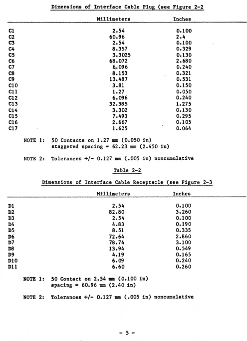
D6 D7 DB D9 DIO Dll [image:13.618.50.546.73.756.2]Table 2-1
Dimensions of Interface Cable Plug (see Figure 2-2
Millimeters 2.54 60.96 2.54 8.357 3.3025 68.072 6,.096 8.153 13.487 3.81 1.27 6.096 32.385 3.302 7.493 2.667 1.625
NOTE 1: 50 Contacts on 1.27 mm (0.050 in)
staggered spacing - 62.23 mm (2.450 in)
Inches 0.100 2.4 0.100 0.329 0.130 2.680 0.240 0.321 0.531 0.150 0.050 0.240 1.275 0.130 0.295 0.105 0.064
NOTE 2: Tolerances +/- 0.127 mm (.005 in) noncumulative Table 2-2
Dimensions of Interface Cable Receptacle (see Figure 2-3 Mi-llimeters 2.54 82.80 2.54 4.83 8.51 72.64 78.74 13.94 4.19 6.09 6.60
NOTE 1: 50 Contact on 2.54 mm (0.100 in) spacing - 60.96 mm (2.40 in)
Inches 0.100 3.260 0.100 0.190 0.335 2.860 3.100 0.549 0.165 0.240 0.260
Figure 2-2
Interface Cable Plug
/#5C
PIN.,__ ___A:oi
r
C
~
~
CZ
tkl
PI~
i
SEE
NOTE I1
...
~-..
.._-u_··-m
i
=t~
lJ
]
(4C5
CI~---J
-,
.
~
1,-->I-P-lN--
CC
- t
=
5
~;~. . . .
[image:14.624.12.589.51.762.2]-
I e
Figure 2-3
[image:15.613.69.582.56.763.2]2.4 Electrical Characteristics
2.4.1 Bidirectional Contr~l Bus Lines
The bidirectional Control Bus is used in two different modes:
Daisy Chain Mode and Radial Mode.
In the Daisy Chain Mode eight bits of information and an optional pa~ity bit shall be tranferred between the host and the selected device.
In Radial Mode each of the eight Control Bus lines shall be used separately for communication with one specific device. In this way, one bit of information is transferred to or from all devices simultaneously. Each device shall have provisions (jumper,
switches, etc) to connect the radial line to anyone of the eight Control Bus lines. The configuration of the bidirectional Control Bus lines is shown in Figure 2-4.
2.4.1.1 Control Bus Drivers
The bus drivers for the parallel informatiOn shall be either three-state or open collector. The driver for the radial signal in the device shall be open collector.
All bus driver outputs for "LOW" level shall sink 24
milliamps minimum. The "LOW" level output voltage shall be 0.5 volt maximum. Driver outputs for "HIGH" level shall have a "HIGH" level output voltage of 2.4 volts minimum, 5.25 volts maximum. A 10 milliamps source current is provided by the 470 ohms terminator discussed in Section 2.4.1.3.
The leakage current in the high impedance state ("OFF" state for open collector drivers) shall not exceed 0.25 milliamp for either "HIGH" or "LOW" level on the Control Bus.
The total number of drivers connected to any Control Bus line shall not exceed ten (one in the host, one in each of the eight devices for the parallel lines, and one in a single device for the radial line).
2.4.1.2 Control Bus Receivers
The maximum "LOW" level input current shall be ~400
microamps. The maximum "HIGH" level input current shall be 80 microamps. The maximum "LOW" level input voltage shall be 0.9 volt. The minimum "HIGH" level input voltage shall be 2.0 volts.
Figure 2-4
Cable Configuration for Bidirectional Control Bus Signals
+sv
,
I
\ 470 / Ohms \ /
Alternative A
(Three-State Drivers for Parallel Lines and
Open Collector
Alternative B
(Open Collector Drivers)
Drivers for Radial Lines)
,
1
. \ To Device\ .
)---x
1/
Logic//\ From Device
.----( ---X
\ I
Logic
I~---x
I
EnableI
I
1\
I \
To Device ) - - - - XI,'
Logic- - - From Device
,
I---X
.--(
I
Logic\
I---x
Enable Open Collector
/ 8 Parallel
\ / 8 Parallel
I
LinesFrom \
I I
LinesI I
x---
)---.---.---.
Host /
I
I
I
I
Logic
1/
\
0 1 Radial LineX----
/
II
)
Jumper/SwitchEnable /
I
)
X---(
0To Host \
Logic \
1\\
To Device.--- ) - - - - X
Host
'/' Logic
---- From Device
, I---x
- ( Logic
\
---X
- - Enable
Open Collector Device o ) ) o
1 Radial Line
Jumper/Switch
\\\ To Device
. - - - - )---X
//
Logic--- From Device
,
,..:.---x
---( Logic
\
I---X
--- EnableOpen Collector
[image:17.621.60.557.74.768.2]2.4.1.3 Control Bus Termination
A 470 ohms resistor, plus or minus 10% shall be installed at the host end of all Control Bus lines (Control Bus Bits 0-7) connected to +5 volts, plus or minus 5%. See Figure 2-4.
2.4.2 Single Ended Lines
The cable configuration of the single ended lines shall ·be as shown in. Figures 2-5 to 2-7.
2.4.2.1 Single Ended Line Drivers
The drivers shall have open collector outputs capable of sinking 40 milliamps at "LOW" levels. "LOW" level output voltage shall not exceed 0.4 volt. The high level leakage current shall not exceed 250 microamps.
2.4.2.2 Single Ended Line Receivers
The receivers shall accept TTL logic levels. For noise immunity the receivers shall have an input hysteresis of 0.4 volt minimum, with a postitive going threshold voltage
between 1.4 and 2.0 volts and a negative going threshold voltage between 0.5 and 1.1 volts. "LOW" level input current shall be -1.2 milliamps or less. The "HIGH" level input current shall be 40 microamps maximum.
2.4.2.3 Single Ended Line Termination
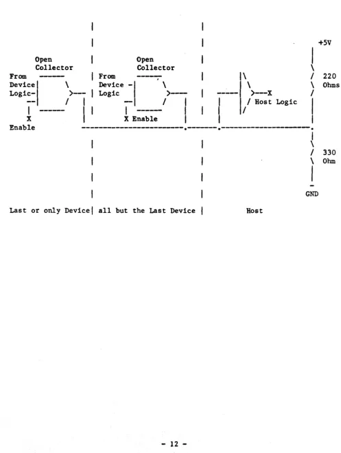
All single ended lines originating at the host shall be terminated at the last device with 330 ohms, plus or minus 5%, to ground and 220 ohms, plus or minus 5%, to +5 volts. All single enaed lines originating at the devices shall be terminated in the same way at the host.
2.4.2.4 Port Enable Termination
Figure 2-5
Cable Configuration for Unidirectional Single Ended Lines From Host (Except Port Enable)
I
\
\ To Device
>----X
1/
Logic\
\ +5V
/
\ To Device
)---x
I
LogieI
\
I
220From \
I
\
Ohmsx---
>---.---.---.
Host
I
Logie
I
Host
Host
[image:19.626.51.542.55.763.2]all but Last Device (if multiple devices)
Figure 2-6
I
I
\ 330
/ Ohms
f
GND
Last or only Device
Cable Configuration for Port Enable
1
\ +5V
I
10k Ohms\
1\
I
.--I
I
\ To Device
)---X
/ Logie
all but Last Device (if multiple devices)
+5V
~
/ 10k Ohms
\
Last or only Device
GND
220 Ohms
330
Figure 2-7
Cable Configuration for Unidirectional Single Ended Lines From Devices
Open Collector From
Device 1
LOg1~:1
1
X
\
>--I
1,
Open Collector From
---
,Device - \
Logic
>---I
I
1
-X Enable
I
+sv
I
\
1\
I
220--:...--1
\---X\
OhmsI
/11
Host LogicI
1
Enable
---.---.---.
{
I
330\ Ohm
I
GND
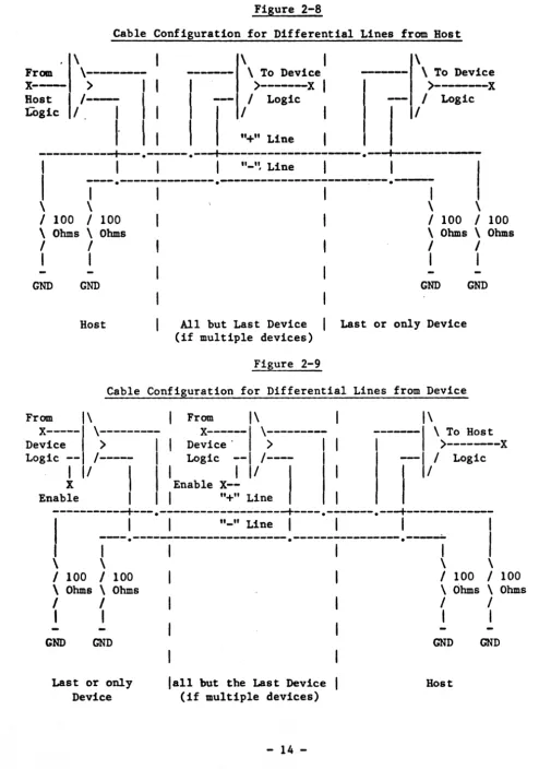
[image:20.624.56.553.102.762.2]2.4.3 Differential Lines
The differential lines drivers and receivers shall operate from a single +5 volts supply. They shall operate at 9.67 MHz and shall be capable of meeting the timing requirements of Sections 5.3 and 5.4 while operating the recommended terminated cable configuration.
The cable configuration of the differential lines shall be as shown in Figures 2-8 and 2-9.
An active signal state is defined as the 11+" line being equal or more postitive than the II_II line. An inactive signal state is
defined as the "_" line-being more positive the the "+" line.
2.4.3.1 Differential Line Drivers
The differential line drivers shall have a three-state output and be capable of sinking or sourcing a minimum of 20
milliamps in the active state. In the inactive or high impedance state, leakage current shall not exceed plus or minus 20 microamps. RS422 compatible line drivers.
2.4.3.2 Differential Line Receivers
The common mod input range capability of the receivers shall be at least +7 to -7 volt. The differential input voltage shall be -0.2 volt minimum and +0.2 volts maximum. RS422 compatible line receivers.
2.4.3.3 Differential Line Termination
Each line of all pairs of differential lines shall be
Figure 2-8
Cable Configuration for Differential Lines from Host
\
\
I
\
From
\ - - - - -
---
\ To Device \ To Devicex--
)I : I
)---XI
>---x
Host
/ - -
-
/
Logic-
/
LogicLOgic
/
I
/
/
, I
,
"+It
Line---+---.---.---+---.---+---I
~
It_I~ Line
----.---.---~-.---
...
I
\
!
/ 100 / 100
\ Ohms \ Ohms
/ 100
I
100\ Ohms \ Ohms
/
/
I
I
GND GND
Host All but Last Device (if multiple devices)
Figure 2-9
/
/
I
I
GND GND
Last or only Device
Cable Configuration for Differential Lines from Device
From
1\
I
From1\
1\
De!~~--
';---1
I
De!~~;~--I
';---1
Logic -- /--- Logic
--I
/----i
1/
,
I
Enablex-!
II
Enable
I
I
"+"
LineI
---1 \
To Hos tI
)---X-1/
Logic---+---.---+----.---.---+---I
I
I
"-It
LineI
I
I
,I
----.---.---.---\ t
t \
I
100I
100 / 100I
100\ Ohms \ Ohms \ Ohms \ Ohms
I
I
I
I
I
I
I
I
GND GND
Last or only Device
fall but the Last Device (if multiple devices)
GND GND
[image:22.620.44.538.59.763.2]Table 2-3
Pin ASsignment
Signal Ground
Pin Pin Signal Name Sisnal Source
1- Ground
Control Bus
2 -10 Bit 0, Select/Attn. Device 0 Host/Device 3 10 Bit
I,
Select/Attn. Device 1 Host/Device 4 10 Bit 2, Select/Attn. Device 2 Host/Device 5 10 Bit 3, Select/Attn. Device 3 Host/Device 6 10 Bit 4, Select/Attn. Device 4 Host/Device 7 10 Bit 5, Select/Attn. Device 5 Host/Device 8 10 Bit 6, Select/Attn. Device 6 Host/Device9 10 Bit 7, Select/Attn. Device 7 Host/Device
11 12 Reserved
13 14 Select Out/Attn. In Strobe Host
15 16 Command Request Host
17 18 Parameter Request Host
19 20 Bus Direction Out Host
21 22 Port Enable Host
23 24 Reserved
25 26 Read Gate Host
27 28 Write Gate Host
29 30 Bus Acknowledge Device
31 32 Index Device
33 34 Sector Mark Device
35 36 Attention Device
37 38 Busy Device
39 38 Read Data
+
Device40 38 Read Data - Device
42 41 Read/Reference Clock
+
Device43 41 Read/Reference Clock - Device
45 44 Wri te Clock
+
Host46 44 Write Clock - Host
48 47 Write Data
+
Host49 47 Write Data - Host
[image:23.627.48.552.58.762.2]3.0 Signal Definitions
This section provides signal definitions and their intended operation and/or status. Relative signal timing and tolerance is defined in Section 5.
Note: The timing diagrams of Section 5 shall take precedence over all other timing definitions.
3.1 Control Bus
The Control Bus shall be used for bidirectional transfer of
information. The direction of transfer shall be determined by the Bus Direction Out signal.
The electrical characteristics of the Control Bus signals are defined in Section 2.4.1 The Control Bus Lines shall be "LOW" for an active signal state and shall be "HIGH" for an inactive signal state.
Throughout the specification of this interface the host shall be in control of the Control Bus. All communications between the host and the selected device shall be determined by the host.
The Control Bus is used in two modes. When Select Out/Attention In Strobe is active, the Control Bus shall be in Radial Mode. When the Command Request, Paramenter Request, or Bus Acknowledge is active, the Control Bus shall be in Daisy Chain Mode.
3.1.1 Radial Mode
Each device shall be assigned a unit number 0-7, by radially attaching the one Select/Attention device (0-7) line as per Table 2-3.
3.1.1.1 Select Out Mode
When both Bus Direction Out and Select Out/Attention In Strobe are active each radial line shall transfer the selection information to the corresponding device.
3.1.1.2 Attention In Mode
3.1.2 Daisy Chain Mode
When in the Daisy Chain Mode, all Control Bus transfers shall consist of a two byte sequence. The transfer is asynchronous and controlled with a handshake protocol. The first byte is
transferred using a handshake between the Command Request Signal and the Bus Acknowledge Signal. The second byte is transferred using a handshake between the Parameter Request Signal and the Bus Acknowledge Signal. Refer to Section 4 for the command .
definitions.
3.1.2.1 Command Out
When both the Bus Direction Out and Command Request are
active the host shall transfer a Command Byte to the selected device.
When bit 6 in the Command Code (first byte) is one, the second byte shall be Parameter Out (see Section 3.1.2.2 and Table 4-1).
When bit 6 in the Command Code (first byte) is zero, the second byte shall be Parameter In (see Section 3.1.2.3 and Table 4-2).
When the state of the Bus Direction Out Signal for the
transfer of the parameter (second byte) does not comply with the definition of bit 6 of the Command Code, this condition shall set the Attention Condition and the Control Bus Error Bit in the General Status Byte (see Section 4.4.1.2).
The condition of the Bus Direction Out Signal being inactive and the Command Request Signal being active is a violation of protocol and may optionally set the Attention Condition and the Control Bus Error Bit in the General Status Byte (see Section 4.4.1.2).
3.1.2.2 Parameter Out
When both Bus Direction Out and Parameter Request are active, the host shall transfer a Parameter Byte to the selected device (see Table 4-1).
3.1.2.3 Parameter In
When the Bus Direction Out Signal is inactive and the
3.1.3 Control Bus Bits 0-7, Select/Attention Device 0-7
The eight Control Bus signals, 0-7, shall be used for communication between the host and the device as defined in Sections 3.1.1 and 3.1.2. Control Bus Bit 0 shall be the least significant bit.
3.2 Control Interface
This group of signals are unidirectional in nature. The electrical characteristics of the control interface lines is defined in Section 2.4.2. All control interface Lines shall be "LOW" for an active signal state and shall be "HIGH" for an inactive signal state.
3.2.1 Port Enable
This signal is normally held active by the host. When this signal is active all devices attached to the interface shall respond to the interface protocol as described by this specification.
This signal may be used to disable all devices when host power is lost and/or as a programmed reset. If the interface cable is being disconnected from a device, the device shall be reset by the active to inactive transition on this line.
When this signal changes from active to inactive all devices shall be deselected within 20 milliseconds maximum except for the write circuitry in each device which shall be disabled within 1
microsecond maximum. The device shall remain deselected while Port Enable is inactive.
Upon detecting Port Enable going inactive each device must go to its Initial State as defined below (also see the vendor
specification). After Port Enable changes from inactive to active and after the initial state is reached the device shall set the Attention Condition.
Initial State This is the state a device shall reach within 90 seconds maximum after being powered up, Port Enable has become active or a Selective Reset Command has been received.
The conditions are:
1. The device shall be deselected.
2. The device shall respond to the Select Out/Attention In Strobe Signal.
3. All parameters of commands with Parameters Out in Table 4-1 shall be reset to zero (except Spin Control - see Section 4.1.8).
-3.2.2 Bus Direction Out
5. All reset table error conditions shall be
reset. If the cause of the error still exists, it shall set the error conditions again.
6. The Initial State bit in Sense Byte 2 shall be
Bet.
The Bus Direction Out Signal is transferred from the host to all attached devices. Bus Direction Out controls the direction of transfer on the Control Bus. When the Bus Direction Out Signal is active, this defines a transfer from the host to the device.
3.2.3 Select Out/Attention In Strobe
This signal is transferred from the host to all attached devices. It has two different functions depending on the state of the Bus Direction Out Signal.
When the Bus Direction Out Signal is active, the signal is Select Out Strobe.
When the Bus ,Direction Out Signal is inactive, the signal is Attention In Strobe.
3.2.3.1 Select Out Strobe
Only one device shall be selected at anyone time. When the Bus Direction Out Signal is active, the active going edge of the Select Out Strobe Signal is used for
selecting/deselecting the device.
When any Control Bus Signal is active and Select Out Strobe transitions to active, the device connected to that specific Control Bus line shall become selected.
When any Control Bus Signal is inactive and Select Out Strobe transitions to active, the device connected to that specific Control Bus line shall become deselected.
When all Control Bus Signals are inactive and the Select Out Strobe transitions to active, all attached devices shall become deselected.
3.2.3.2 Attention In Strobe
When the BUB Direction Out Signal is inactive, the Attention In Strobe shall be used to gate the device's internal
3.2.4 Command Request
This signal initiates the handshake control from the host to the selected device. The active state of this signal signifies the transfer of the first byte of each two-byte transfer. Until the receipt of Bus Acknowldge, the Command Request Signal shall remain active.
3.2.5 Parame.ter Request
This signal is also a handshake control line from the host to the selected device. The active state of this signal for a Parameter Out Command indicates that the output Parameter Byte is valid on the Control Bus. The active state of this signal for a Parameter In Command requests the selected device to place the Parameter Byte on the Control Bus. Until the receipt of Bus Acknowledge, the Parameter Request Signal shall remain active.
3.2.6 Bus Acknowledge
This signal is returned from the selected device to the host. The Bus Acknowledge Signal has two functions.
When the Control Bus is used in Radial Mode (Select Out/Attention In Strobe active), the selected device shall make the Bus
Acknowledge Signal active to acknowledge its selection.
When the Control Bus is used in Daisy Chain Mode, the Bus
Acknowledge Signal performs the asynchronous handshake with the Command Request Signal or the Parameter Request Signal.
3.2.7 Busy
The Busy Signal shall change to the active state before the active going edge of the Bus Acknowledge of a Time Dependent Command (see Section 4.0) that causes the device to become busy. The busy Condition will occur during power up sequencing, seeking, or execution of diagnostics.
The busy to not busy transition within the device shall set the Attention Condition within the device (see Section 3.2.8).
If Command Request becomes active when the Busy signal is already active the device will not respond with Bus Acknowledge before the function is completed and Busy is made inactive.
Note:
3.2.8 Attention
The Busy Interface signal is different from the Busy Executing status bit (see Section 4.4.1.7).
The Attention Signal shall be made active by a devicet if the device's internal Attention Condition is set to onet and if Attention is enabled (see Attention Control Command Section 4.1.1). The Attention Condition shall be set if the device
requires service from the host. The detailed conditions to set the Attention Condition are defined in Section 4.
The Attention Condition of the selected device shall only be reset by'the Clear Attention Command or the Clear Fault Command. Issuing the Clear Fault Command shall reset only those error status bits and the resulting Attention Condition if the error condition can be reset. A Clear Attention Command shall reset the Attention
Condition independent of error conditions.
3.2.9 Index
Index is a signal that indicates to the host that a reference point or index area is passing under the heads of the selected device. One Index Pulse shall be generated by the selected device per revolution of the recording media.
Whenever the device is readYt a valid Index Signal shall be transferred from the selected device to the host.
3.2.10 Sector Mark
The Sector Signal establishes rotational reference points on the recording surface. Each track may be divided into sectors with the initial sector ("Zero") starting coincident with the Index Pulse. All subsequent sectors start coincident with the active going edge of a Sector Pulse. When the Index Pulse is activated t the Sector Pulse is omitted.
Whenever the device is readYt a valid Sector Mark Signal shall be transferred from the selected device to the host.
In the event that the sector signal is not an even division of this track capacitYt the last sector shall be elongated to include the remainder. Short sectors are not allowed.
3.2.11 Read Gate
The Read Gate Signal is transferred from the host to the selected device.
The Read Gate Signal enables and synchronizes the read circuitry to transfer the serialized data information on the Read Data lines from the recording medium.
3.2.12 Write Gate
The Write Gate Signal enables the write circuitry in the device to transfer the serialized information on the Write Data lines to the recording medium. Note, a write operation shall not take place unless a write enable condition has been established by a previous Write Control Command.
3.3 Read/Write Signals
This ~ection describes the signals used when transferring data to and from the host. These signals are only valid if a device is
selected. All of these signals are driven differentially (see Section 2.4.3). All data sent to the device or host shall be Non-Return-to-Zero (NRZ).
3.3.1 Read Data
When Read Gate is active, the Read Data lines transfer the serial NRZ read data from the selected device to the host. This data is synchronized with Read Clock. The Read Data signal shall be static when Read Gate is not active.
3.3.2 Read/Reference Clock
The Read/Reference Clock is transferred from the selected device to the host. This signal shall transfer Read Clock when Read Gate is active. Read Clock shall be synchronous with the serial NRZ read data. This signal shall transfer the Reference Clock at all other times. The transitions between Read Clock and Reference Clock shall be glitch free.
3.3.3 Write Data
When Write Gate is ~ctivet the Write Data lines shall transfer the serial NRZ write data from the host to selected device for
recording. The serial write data shall be synchronized to the Write Clock. This signal shall be held static at all times except when Write Gate is active.
3.3.4 Write Clock
Write Clock shall be used by the selected device to properly phase the Write Data lines while recording. Write Clock shall be
4.0 Command Structure
All command, status, and parameter information passed between the
selected device and the host shall be transferred via the Control Bus and shall conform to the command protocol defined in this standard.
The command protocol requires that each command sequence consists of a two byte transfer. The first byte, the Command Byte, shall always be transferred from the host to the selected device. The second byte, the Parameter Byte, may be transferred from the host to the selected device or from the selected device to the host. The direction of the transfer of the Parameter Byte is determined by the state of the Bus Direction Out signal.
The Command Byte therefore, indicates the particular function that the selected device is to perform. This may include functions such as
accepting parametric information from the host, performing requested head motion, or reporting specific status conditions. The Command Byte also conditions the device as to the direction of the transfer of the
Parameter Byte portion of the command sequence.
The Parameter Byte completes the command sequence by providing the parameter or status information demanded by the Command Byte. In cases where the Command Byte is sufficient to indicate the complete nature of the command, the General Status Byte is transferred as Parameter Byte to complete the command sequence.
Below all defined command sequences are specified. They are divided into two groups: one which r~quires the Parameter Byte transferred go the device (Parameter Out) and one which requires the Parameter Byte transferred to the host (Parameter In).
There are two kinds of commands:
Immediate Commands and Time Dependent Commands.
For Immediate Commands the active going edge of the second Bus Ackowledge shall not be generated until the required action has been performed. In the case that action is not performed, Attention Condition shall be set prior to the active going edge of the Bus Acknowledge Signal that is returned as a response to Parameter Request.
For Time Dependent Commands the Attention Condition shall be set when the action for the Time Dependent Command is completed. The resetting of the Attention Condition by tbe Immediate Command, Clear Fault or Clear
Attention, completes the Time Dependent Command.
All commands, once in progress, shall proceed to completion utlizlng parameters established prior to tbe issuance of the command.
While all commands are defined individually. there are logical groupings of commands that represent functional operations. For example. the loading of parameter information (cylinder address) and the execution of a particular operation (seek). Unusual command sequences within such groupings may result in violations of an implied protocol and will cause responses which are implementation dependent and will vary among vendors.
Table 4-1 Commands With Parameters Out
Function
Attention Control
ll.rite Control
Set Upper Cyl. Address Set Lower Cyl. Address Select Moving Head
Load Attribute Number Load Device Attribute Spin Control
*
Load Sec. Pulses Per Track High
Load Sec. Pulses Per Track Medium
Load Sec. Pulses Per Track Low
Load Test Byte
Command Code
40 Hex
41 Hex
42 Hex
43 Hex
44 Hex
50 Hex
51 Hex 55 Hex
59 Hex
SA Hex
5B Hex 6F Hex
All unused bits in parameters shall be zero.
Parameter Out
Bit 7
o -
Enable Attention 1 - Disable Attention Bit 71 - Write Enable
o -
Write DisableMSB of Cylinder Address LSB of Cylinder Address Head Number
Address Byte Information Byte Bit
7
1 - Spin Up
o -
Spin DownMSB of Sector Pulses Per Track
MedSB of Sector Pulses Per Track
LSB of Sector Pulses Per Track
Test Byte
[image:33.621.56.542.57.389.2]Function
Report "Illegal Cmd.n
Clear Fault Clear Attentio.n Seek
*
Rezero
*
Report Sense Byte 2** Report Sense Byte 1** Report General Status**
Report Device Attribute Set Attention *
Selective Reset * Partition Track * Report Cyl. High Report Cyl. Low Report Test Byte
Table 4-2
Commands With Parameters In
Command Code Parameter In
00 Hex General Status
01 Hex General Status
02 Hex General Status
03 Hex General Status
04 Hex General Status
OD Hex Sense Byte 2
OE Hex Sense Byte 1
OF Hex General Status
10 Hex Device Attribute Byte
11 Hex General Status
14 Hex General Status
16 Hex General Status
29 Hex MSB of Cylinder Address
2A Hex LSB of Cylinder Address
2F Hex Echo Byte
The commands with "*" appended are Time Dependent Commands that set an Attention Condition upon completion.
[image:34.618.62.542.65.374.2]4.1
Commands With Parameter OutAll commands defined in this section require a Parameter Byte to be
transferred to the device. These commands are summarized in Table
4.1.
-4.1.1 Attention Control (Command Code 40 Hex)
This command shall condition the selected device to enable or
disable its attention circuitry based on the value of the Parameter Byte as shown below.
7 6 5 4
o
o
o
¢
o -
Enable Attention 1 - Disable Attention3 2 1
o
o
o
o
o
This command allows the host to selectively ignore attention
requests from certain devices on the interface. This might be done in response to a device that generates spurious attention requests due to a malfuntion.
The Enable Attention Command shall cause the selected device to gate its internal Attention Condition onto the party line ("wired OR") Attention Signal. The Disable Attention Command shall cause the selected device to disable the gating of the internal Attention Condition onto the party line Attention Signal. This command shall have no impact on the function of the radial status returned with
the Attention In Strobe Signal (see Signal 3.2.3.2).
Devices shall be initilized with the Attention circuitry enabled.
4.1.2 Write Control (Command Code 41 Hex)
This command shall condition the selected device to enable or disable its write circuitry based on the value of the parameter Byte as shown below:
7 6 5
o
o
¢
1 - Write Enable
o -
Write Disable4
o
3o
2o
1o
o
o
This command is used in conjunction with the Write Gate Signal and therefore merely enables the write circuitry while the Write Gate Signal activates the circuitry at the proper time. An active Write Gate Signal while the device's write circuitry is disabled shall result in no data being recorded.
A Write Control Command execute during a write operation is a violation of protocol.
4.1.3 Set Upper Cylinder Address (Command Code 42 Hex)
This command shall condition the selected device to accept the Parameter Byte as the most significant Byte of a cylinder address.
This command is used in conjunction with the Seek Command (see Section 4.2.4) and therefore is a means of supplying the most significant byte of a target cylinder address.
This command shall not cause any head motion. Loading a cylinder address outside the range of a device shall not cause an error unless a subsequent Seek Command is issued to that illegal cylinder.
Devices shall be initialized with the target cylinder address equal to zero.
4.1.4 Set Lower Cylinder Address (Command Code 43 Hex)
This command shall condition the selected device to accept the Parameter Byte as the least signficant byte of a cylinder address.
This command is used in conjunction with the Seek Command (see Section 4.2.4) and therefore is a means of supplying the least significant byte of a target cylinder address.
This command shall not cause any head motion. Loading a cylinder address outside the range of a device shall not cause an error unless a subsequent seek command is issued to that illegal cylinder.
Devices shall be initialized with the target cylinder address equal to zero.
4.1.5 Select Moving Head (Command 44 Hex)
This command shall condition the selected device to. accept the Parameter Byte as the binary address of the head selected for read or write operations. This command shall enable the moving heads and shall disable the fixed heads.
A Select Moving Head Command issued during a read or write operation is a violation of protocol.
The device shall set the Attention Condition and the Illegal Parameter Bit in the General Status Byte upon receipt of a head address out.side the head address range of the device.
4.1.6 Load Attribute Number (Command Code SO Hex)
This command shall condition the selected device to accept the Parameter Byte as the number of a Device Attribute as defined in Table 4-3. This command prepares the device for a subsequent Load Device Attribute Command or Report Device Attribute Command (see Sections 4.1.7 and 4.2.9). This command may be issued at any time.
4.1.7 Load Device Attribute (Command Code 51 Hex)
This command shall condition the selected device to accept the Parameter Byte as the new value of a Device Attribute. The number of the Device Attribute must have been previously defined by the Load Attribute Number Command (see Section 4.1.6).
4.1.8 Spin Control (Command Code 55 Hex)
This command shall condition the seleted device to enter a spin up or spin down cycle based on the value of the Parameter Byte as shown below.
7 6 5 4 3 2 1 ·0
0 0 0 0 0 0 0
I
I
1 - Spin Up
o -
Spin DownA spin up cycle shall consist of starting the rotation of the spindle. A spin down cycle shall consist of stopping the rotation of the spindle.
Upon completion of a spin control cycle the device shall set the Attention Condition. Issuing a spin up command to a device whose spindle is already at full speed or issuing a spin down command to a device whose spindle has already stopped shall also set the Attention Condition.
The Spin Control Command is a Time Dependent Command and as such shall set the Busy Executing bit in the General Status Byte (see Section 4.4.1.7) while command execution is in process. Also, the device shall exercise appropriate control over the Busy signal at the interface (see Section 3.2.7).
A spin down cycle shall cause the repositioning of the moving head(s) over the landing sone and stop the rotation of the
spindle. If the device detects that it cannot successfully seek to the landing zone it shall set the Attention Condition and set bit 0 of Sense Byte 1.
[image:37.627.56.558.19.788.2]4.1.9 Load Sector Pulses Per Track High (Command Code 59 Hex)
This command shall condition the selected device to accept the Parameter Byte as the most significant byte of a 24 bit number that represents the total number that will control the number of sector pulses between (but excluding) Index Pulses generated by hard sectored devices when a Partition Track Command (see Section 4.2.12) is executed.
This command is used in conjunction with the Partition Track Command and is a means of supplying the most significant byte of the Sector Pulses Per Tr~ck value.
Prior to completion of the execution of the Partition Track Command. the co