NOVEMBER 1965
TECHNICAL MANUAL
FDR
3110411-10 REV E 8-68
DE-211/DE-291
DATA ELECTRDNICS
REVIEWED BY
~c
~
ENG'NEEA
APPROVED BY --=t:::.=:..:....!.
)::...:-'-L~~~,==' ~~~=====
eECT;;:;::SNAGER
LIST DF EFFECTIVE PAGES
TABLE DF CDNTENTS
Section Paragraph
I GENERAL DESCRIPTION
1-1 1-2 1-3 1-4 1-5 1-6 1-7
Introduction. . . . . . Scope . . . . Model Design.ations . . . ," . .
Purpose and Basic Principles . . . .
Purpose . . . . Basic Principles . . . .
Special Features
II INSTALLATION
2-1 2-2 2-3 2-4 2-5 2-6 2-7 ,2-8 2-9 2-10 2-11 2-12 2-13 2-14 2-15 2-16 2-17 2-18 2-19 2-20 2-21 2-22 2-23 2-24 2-25 2-26 2-27 2-28
Introduction. . . .. . . . Scope . . . ' . . . . Unpacking . . . .
Power Requirements. . . . Installation . . " . . . .
Cabling . . . .
Input Signal Requirements . . . ; . . . . Input Signal Voltage Levels . . . . Input Signal Timing . . . ' •.
Write Data . . . , . . . . " . . . . W rite Strobe . . . • . . . .
Write Re set. . . .. . . .
Write Permit . . . " . . . .
Read Permit . . . . HI/La Density . . . ' . . . , ; .. " . . . . Odd/Even Parity . . . . Forward/Reverse . . . .
Run/Stop· . . . .
Forward/Stop (Option). . . • . . . . Reverse/Stop (Option) . . . .
Rewind . . . .
Rewind and Lockout . . . . Output Signal Characteristics . . • . . .
Output Signal Voltage and Current Levels. . . . Output Signal Timing. . . • . . . . Read Data . . . . Read Clock . . . . Vertical Parity Error (Option) . . . .
Section Paragraph
II 2-29
2-30 2-31 2-32 2-33 2-34 2-35 2-36 2-37 2-38 2-39
Write Check Error (Option) . . . . Write Enable Status • . . . 0 • • • • 0 • • LP Error (Special Feature) . . . 0 • • • • • • • Tape Transport Status Outputs . . . .
Beginning-of-Tape (BOT) . . . ; . . . . End-of-Tape (EOT) . . . 0 • • • • • High/Low Density Status . . . !J • • • • • • • •
Ready . . . " .. " . . . .
Rewinding . . . . Unit Select . . . ." . . . .
Select and Remote Indicator . . . ' . . . .
2-10 2-10 2-10. 2-11 2-11 2-11 2-11 2-11 2-11 2-11 2-11
III OPERATION
3 -1 Introduction. . . .. . '. 3 -:' 1
3-2 Operating Modes . . . .. . . .. 3-1
3-3· Write Check. Mode . . . 0 • • 0 • • • 0 0 • 0 • . 0 • • • • o. 3-1
3-4 Write Only Mode . . . '. . .. 3-1
3-5 Read Only Mode 0 • • • • • • • • • • • • • • • • • • • • • • • • '. • • • • • • 3-1 3-6 Write Signal Conditioning. . . .. . . . . .. . . • . . . .. 3-1
3 -7 Write Data . . . . .. . . .. 3-2
3-8 Write Power . . . 0 • 0 , , , • , , , • , , , • • • , , , , • , , , , • " • " 3-2
3-9 Write Reset . . . 3-2
3-10 Read Signal Conditioning . . . , , .. , .. , , . , . , , , . , . , . .. 3-3
3-11 Read Data. . . . 3-3
3-12 Strobe Generation . . . , . , .. , .. 0 , , . • • • • , , • • , • , , • • : . • • 3-3 3-13 Error Checking, . . . ', , . , , , 0 • 0 • • • • , 0 0 • 0 0 • 0 0 • 0 • • 3-4 3-14 Vertical Parity.Check 0 0 0 • 0 • • 0 0 • 0 0 • • ' 0 0 • 0 0 • 0 0 0 0 0 • 0 3-4 3-15 Rate Check 0 0 0 0 0 0 0 0 0 0 0 0 0 0 0 0 0 • 0 0 0 0 0 0 0 0 0 0 0 0 0 0 0 0 0 3-4 3-16 Echo Check 0 0 0 0 0 0 0 0 0 0 0 0 0 0 0 0 • 0 0 '0 0 0 0 0 0 0 0 0 0 0 0 0 0 0 0 3-4
IV THEORY OF OPERATION
4 -1 Introduction. 0 0 0 • 0 0 0 0 • 0 0 0 • 0 0 0 • • • • • 0 o' 0 0 • 0 0 • • 0 0 • • 0 0 4-1 4 - 2 Logic Diagram. . 0 0 0 • 0 • • 0 0 0 0 o· 0 0 0 0 0 0 0 0 0 0 • 0 0 0 • 0 • • • 4-1
4-3 Logic Element Identificatiollo . . . 0 0 • • 0 • • 0 • • • • 4-1
Section Paragraph
IV
4-12
4-13
4-14
4-15
4-16
4-17
4-18
4-19
4-20
4-21
4-22
4-23
4-24
4-25
Write Data
...
'... .
Write Reset . . . .
4-3
4-3
Write Register DC Reset. . . .. 4-4 1'est Deskew. . . ..
4-4
Write Head Power. . . .. 4-4 Read Logical Sequence . . . ..
4-4
Read Pernlit . . . .. 4-4 Read Data. . . 4-4 Read Strobe. . . • . . . .. 4-6 Error Check Options. . . • . . .
4-7
Vertical Parity Check. . . • . . . .• . . . ..
4-7
Rate Check . . . ..
4-7
Echo Check. . . ..
4-8
Write/Check Error. . . • . . . ..
4-8
V MAINTENANCE
5-1
5-2
5-3
5-4
5-5
5-6
5-7
5-8
5-9
5-10
5-11
5-12
5-13
5-14
5-15
5-16
5-17
5-18
5-19
Introduction . . . \I • • • • • \II • • • • • • • •
Test Equipn1ent \II • \II • • • • • \II • • • • • • \II • • • • • • • • • • • • • • • • Adjustment Schedule • . . . • . . . Adjustment Procedures • . . . Clipping Level. . . • . . . . Read Deskew . . . \II • • \II • • • • \II • • • • • • • • • • • \II \II • • • • • • •
Write Check . . . \II • • • • • • • • • • • • • • • •
Write Deskew . \II • \II • • \II • • • • • • • • • • \II • • • • • • ' • • • • • \II \II • •
Read Strobe Delay . . . • . . . • . . . • Rate Check Reference Time . . . • . . . Alternate Adjustment Procedure • . . .
Gene~al .. _, \II \II • • • • • • \II • • • • \II • • • • • • • \II • • • • • • \II • • • • •
Clipping Level. . . ... . . . Read Deskew . . . \II • \II • \II • • • • • • • \II • • • • • • • • • • • • • • • •
Write Check . \II . . . \II • • • • • • • • • • • • \II •
Read Strobe Delay and Rate Check Reference Time . . . . Troubleshooting Procedure • . . . '.' Preliminary Tests . . . . Troubleshooting Tables . . . • . . . • . . .
5-1
5-1
5-1
5-2
5-2
5-4
5-11
Section Paragraph
VI CIRCUIT DESCRIPTIONS
6-1 Introduction . . . .
VII DRAWINGS
7-1 Introduction . . . • . . .
VIII SPECIAL FEATURES
Figure
2-1 2-2
2-3
3-1 3-2· 3-3
4-1 4-2 4-3 4-4
4-5
4.-6
5.-1 .3-2 5-3
5-4
5-5 5-6 5-7
8-1 Introduction. " " " " " " ~ " " " " " " "',, " '. " " " " '. " " " "-,, " " " " " '. " " "
LIST'DF ILLUSTRATIDNS
Title
pea
Locations " " " , " " " " " , " " " " " " " " " " " " " " " " " " " "." " " " " " " " " "Timing Requirements for Write Data, Write Strobe,
and Run/Stop Inputs . . . ' . . . ' . . . . Timing Requirements for Write Permit, Forward/Reverse,
Run/Stop, Forward/Stop, and Reverse/Stop Inputs . . . .
Write Signal Conditioning, Block Diagram . . . . Read Signal COl,1ditioning, Block Diagram . . . ' . . . • . . . , . Error Check Circuits, Block Diagram . . . . '.; . . . • . .
Typical-L~ogic Symbol . . , . . . • . . .. . . , ,'. . . ... ' . '.' ;... . . • . Read Deskew Timing . . . ' ... ' . . . . . Rate Error Check, Block Diagram . . . . Rate Error Timing . . . , . . . ' . . . ' . . . . Echo Check, Block Diagram . . . . Echo Check Timing. . . .' . .'. . . .. . . . . •. . ~ . . . . . .' . . . .
Clip Level and Strobe Delay Potentiometers . . . • . . . Read Amplifier Adjustments . . . • . . . ; . . . . Read Deskew Reference Track Selection . . . . Read Deskew Potentiometer Location . . . . Write Deskew Potentiometer Location . . . . Read Strobe Delay Timing . . . . Rate Check Reference Timing . . . ' . . . • . •
6-1
7-1
8-1
2-2
2-6
2-8
3-2 3-3 3-4
4-1
4-5
4-9 4-9 4-10 4-10
Table
1-1
2-1 2":2 2-3 2-4 2-5 2-6 2-7 2-8
5-1 5-2 5-3 5-4 5-5 5-6 5-7 5-8 5-9 5-10
6-1
7-1
8-1
LIST DF TABLES
Title
Data Electronics Addenda
Power Supply Output . . . . PCB Part Nun1ber s . . . . System Input Connections (Typical) • . . . System Output Connections (Typical) . • . . . ',' Data Electronics to Read Head Interconnections . . . . Data Electronics to Write Head Interconnections . . . . Data Electronics to Tape Transport Interconnections . . . . Data Electronics to Power Supply Interconnections . . . .
Required Test Equipment . . . • Read Amplifier Adjustments . . . . Read Deskew PCB Location . . . • . . . Write Amplifier PCB Location . . . . Read Strobe Delay Time . . . ',' . . . . Rate Check Reference Time . . . • . . . Test Deskew Input Requirement . . . .
Input Signals . . . .
Write Section Troubleshooting Procedure • • . . . • . . . . ' . . • . . . • '.' Read Section Troubleshooting Procedure • . . . • . . .
List of Circuit Descriptions. . . .
List of Drawings . . . .
Data Electronics Special Features . • . . . • . • . . • . . .
1-2
2-1 2-4 2-12 2-13 2-14 2-15 2-16 2-17
5-1 5-6 5-9 5-12 5-1.7 5-19 5-22 ,5-23 5-24 5-25
6-1
7-1
SECTIDN I
GENERAL DESCRIPTIDN
1-1. INTRODUCTION.
1-2. SCOPE.
This technical manual describes the installation, operation, theory of operation and maintenance of the DE-211 and the DE-291 Data Electronics.
1-3. MODEL DESIGNATIONS.
DE-211
Data Electronics---J....I
Tl1 .
Single Speed,Series 2 0 0 - - - -....
J
7 TrackUnshared
DE-291
Data Electronics _ _ _
T...
1F
Single Speed,Series 200 _ _ _ _ _ _ --.1-:- 9 Track
Un shared
1-4. PURPOSE AND BASIC PRINCIPLES.
1-5. PURPOSE.
The Data Electronics card cage is wired, as shown on the Data Electronics Logic Diagram, to accommodate circuit board assemblies which provide the circuitry required to read, write, and check digital data. Seven-track tapes are bilaterally interchangeable with
tapes prepared onffiM 729 tape transports. Nine-track tapes are bilaterally interchangeable
1-6. BASIC PRINCIPLES.
The card cage is wired to actommodate circuit boards which will read and write on either 7 or 9 tracks. Wiring is also included to accommodate circuit boards which will per-form Vertical Parity Check, and Echo and Rate Checks.
Circuit board assemblies included in the card cage are determined by tape speed, bit packing density, number of tracks, error checking options, bidirectional read capability, and special features.
1-7. SPECIAL FEATURES.
The following special features (SF) are documented in Section VIII of this manual.
SF 1: Special Positive Input/Output Levels (Dual Density).
SF2: Vertical Parity Generate (7 Track).
SF3: Vertical Parity Generate (9 Track).
SF4: Longitudinal Parity Check.
SF5: Longitudinal Check Character Generate.
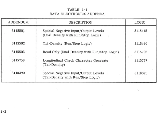
Addenda, which include special logic diagrams, are prepared to document special features not included in this manual. Table 1-1 is a partial list of addenda.
TABLE 1-1
DATA ELECTRONICS ADDENDA
ADDENDUM DESCRIPTION LOGIC
3115501 Special Negative Input/Output Levels 3115445
(Dual Density with Run/Stop Logic)
3115502 Tri-Density (Run/Stop Logic) 3115446
.3115503 Read Only (Dual Density with Run/Stop Logic) 3115795
3115758 Longitudinal Check Character Generate 3115757
(Tri -Density)
3118390 Special Negative Input/Output Levels 3118323
[image:10.620.34.563.393.762.2]2-1. INTRODUCTION.
2-2. SCOPE.
SECTIDN II
INSTALLATIDN
This section provides information on unpacking, power requirements, installation and cabling. Input signal requirements and output signal characteristics are also described in this section.
2 -3 . UNPACKING.
The Data Electronics is installed with the Ampex Tape Transport in the Tape Memory System enclosure. When no enclosure is supplied, the Data Electronics is shipped in custom designed crating. No special unpacking instructions are required. All equipment should be inspected for shipping damage prior to the application of power.
2-4. POWER REQUIREMENTS.
Power for the Data Electronics is supplied by the Ampex Logic Power Supply, which is a separate assembly. The power supply provides three regulated voltage outputs and two unregulated voltage outputs. The power supply requires a maximum input power of 345 watts
with all outputs at the full load shown on Table 2 -1. If the Ampex Logic Power Supply is not
used, provision must be made to supply the voltages listed in Table- 2-1 at the required
cur-rent and regulation.
TABLE 2-1
POWER SUPPLY OUTPUT
REGULATED VOLTAGE CURRENT
+12V +4.5 Amp
-12V -5.0 Amp
- 6V ±1.5 Amp
UNREGULATED VOLTAGE CURRENT
+24V +0.1 Amp
-24V -0.1 Amp
REGULATION
1%
1%
2%
REGULATION
10%
t-J I t-J
"'0
O"Ij
to ...
t"'~ o
t-i
() ro
III
'"" t-J
...
o I ::s ~
CIl ~ c " <n ~ >-~ >-~ >-~ >-~ >-'" t-'" Cl tIl 0 tIl 0 tIl 0 tIl ( l 0 0 0 0 5:i 5:i to
READ AMPLIFIER ([RACK 1) ~ 0
READ AMPLIFIER (TRACKS 2 & 3) ~ 0 READ AMPLIFIER (TRACKS 4 & 5) ~ 0
--READ AMPLIFIER ([RACKS 6 & 7) ~ 0
READ AMPLIFIER (TRACKS 8& 9) ~
0
SELECT LOGIC *
STROBE GENERATOR
EXCLUSIVE OR *
EXCLUSIVE OR *
EXCLUSIVE OR *
ERROR CHECK *
OUTPUT DRIVER
OUTPUT DRIVER
INPUT BUFFER
INPUT BUFFER
~ O ~ 0 ~ 0 ~ 0 S§ S§ ~ S§ ~ ~ S§ ~ S§ Eil
~
~
BtIj'T' tIjt"''''''' ItIj~ t-JO> ~...,o -~~o
~o
CI.l>
READ DESKEW ([RACK 1)
READ DESKEW (TRACK 2)
READ DESKEW (TRACK 3)
READ DESKEW (TRACK 4)
READ DESKEW (TRACK 5)
READ DESKEW (TRACK 6)
READ DESKEW (TRACK 7)
READ DESKEW (TRACK 8)
READ DESKEW (TRACK 9)
WRITE AMPLIFIER (TRACK 1)
WRITE AMPLIFIER (TRACK 2)
WRITE AMPLIFIER (TRACK 3)
WRITE AMPLIFIER (TRACK 4)
WRITE AMPLIFIER (TRACK 5)
WRITE AMPLIFIER (TRACK 6)
WRITE AMPLIFIER (TRACK 7)
WRITE AMPLIFIER (TRACK 8)
WRITE AMPLIFIER (TRACK 9)
WRITE POWER GATE
'" '" .... on '" " 00 '0 .... o .... .... .... '" .... w .... .... .... on .... '" .... " .... 00 .... '0 '" a .., ....
..,
..,..,
'" '" ....'"
>-~ >-~>-'"
>-'" t-'" Cl tIl 0 tIl 0 tIl ( l 0 0 0 0 5:i 5:i toREAD AMPLIFIER (TRACK 1)
'"
0READ AMPLIFIER (TRACKS 2 & 3) ~ 0 READ AMPLIFIER (TRACKS 4 & 5) ~ 0 READ AMPLIFIER (TRACKS 6 & 7)
'"
0SELECT LOGIC *
STROBE GENERATOR
EXCLUSIVE OR *
EXCLUSIVE OR *
ERROR CHECK *
OUTPUT DRIVER
OUTPUT DRIVER *
INPUT BUFFER
INPUT BUFFER
'"
0'"
O6
S§ ~ ~ ~ ~ ~ S§ 2iJsz
~
_,.,..-....J t:J •• J ItIjt"''''''' ItIj~ t-JO> ~...,O -~~
o
~o
CI.l>
READ DESKEW (TRACK 1)
READ DESKEW (TRACK 2)
READ DESKEW (TRACK 3)
READ DESKEW (TRACK 4)
READ DESKEW (TRACK 5)
READ DESKEW (TRACK 6)
READ DESKEW (TRACK 7)
WRITE AMPLIFIER (TRACK 1)
WRITE AMPLIFIER (TRACK 2)
WRITE AMPLIFIER (TRACK 3)
WRITE AMPLIFIER (TRACK 4)
WRITE AMPLIFIER (TRACK 5)
WRITE AMPLIFIER (TRACK 6)
WRITE AMPLIFIER (TRACK 7)
I
WRITE POWER GATE I
2-5. INSTALLATION.
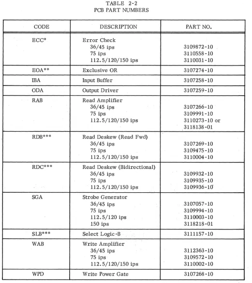
Typical Outline and Installation drawings are provided in the drawing sections of the Tape Transport technical manuals. Figure 2-1 shows typical printed circuit board (PCB) assembly locations for 7-track and for 9-track Data Electronics. Mnemonic designations, as
shown on the Logic Diagram, are provided. Table 2-2 lists the coded designation which appears on the ejector tab of the PCB's and provides the part numbers according to basic tape speeds.
2-6. CABLING.
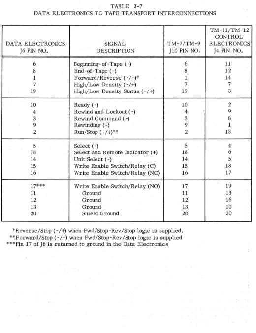
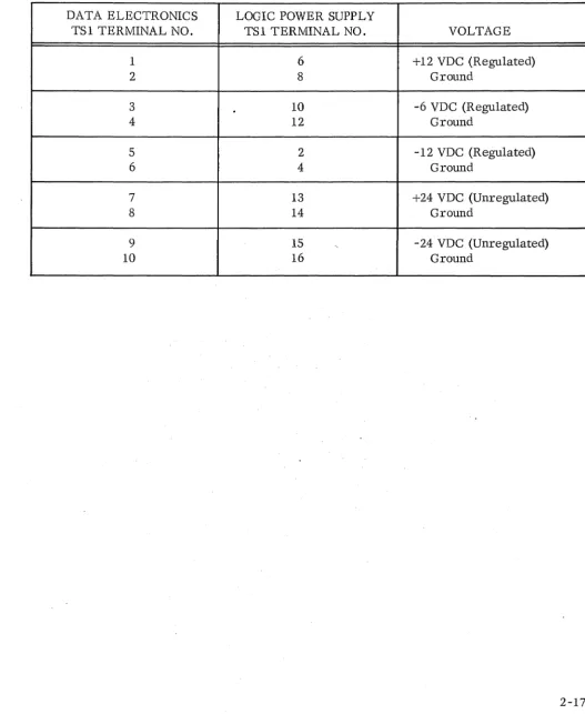
Cabling diagrams for TM-72ll, TM-92ll, and TM-1l2ll Tape Memory Systems are provided in the drawing sections of the tape transport technical manuals. The TM -11211 diagram is also used for TM-122ll systems. Inputs to the system and outputs from the sys-tem are connected to the Data Electronics via the connectors on the Input/Output Panel as shown in Tables 2-3 and 2-4, respectively. These inputs and outputs supersede those listed in the Tape Transport manual. Connections from the read heads are as shown in Table 2-5 and connections to the write heads in Table 2-6. Table 2-7 lists connections to the Tape Transport. Table 2-8 lists connections to the Logic Power Supply. Tables 2-3 through 2-8 are located at the end of this section.
2-7. INPUT SIGNAL REQUIREMENTS.
2-8. INPUT SIGNAL VOLTAGE LEVELS.
The following signal voltage levels apply to all input signals (the input impedance is 2300 ±1l5 ohms returned to -3.8 volts).
TRUE Level: -12 (+3, -13) volts
; FALSE Level: O. 00 fl. 25 volts
NOI.
When non-standard input levels are provided, special Input Buffer PCBs and wiring changes are required.
2-9. INPUT SIGNAL TIMING.
TABLE 2-2 PCB PART NUMBERS
CODE DESCRIPTION PART NO.
ECC* Error Check
36/45 ips 3109872-10
75 ips 3110558-10
112.5/120/150 ips 3110031-10
EOA** Exclusive OR 3107274-10
IBA Input Buffer 3107258-10
ODA Output Driver 3107259-10
RAB Read Amplifier
36/45 ips 3107266-10
75 ips 3109991-10
112.5/120/150 ips . 3110273-10 or
3118138-01
RDB*** Read Deskew (Read Fwd)
36/45 ips 3107269-10
75 ips 3109475-10
112.5/120/150 ips 3110004-10
RDC*** Read Deskew (Bidirectional)
36/45 ips 3109932-10
75 ips 3109935-10
'. 112.5/120/150 ips 3109936-1G
SGA Strobe Generator
36/45 ips .3107057-10
75 ips 3109994-10
112.5/120 ips 3110003-10
150 ips 3118218-01
SLB*** Select Logic ~B ' 3111157-10
WAB Write Amplifie'r" .
36/45 ips 3112363-10
75 ips 3109572-10
112.5/120/150 ips 3110002-10
WPD Write Power Gate 3107268-10
*The Error Check (ECC) PCB is supplied for the Echo and Rate Check option. **Two Exclusive OR (EOA) PCBs are supplied for the Vertical Parity Check option. ***Read Deskew (RDB) PCBs are replaced by Bidirectional.Read Deskew (RDC) PCBs
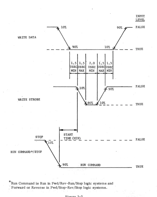
[image:14.620.38.560.75.658.2]2-10. Write Data. (See Figure 2-2.) A minimum interval of 1.5 Ilsec is required between the 90-percent point of the Write Data leading-edge transition and the 10-percent point of the next Write Strobe leading-edge transition.
A minimum interval of 1.5 Ilsec is required between the 90-percent point of the Write Strobe trailing-edge transition and the 10-percent of the next Write Data leading-edge transition.
To write a series of ONE's, the Write Data input may be held at the TRUE level for the entire se:J;"ies.
2-11. Write Strobe. (See Figure 2-2.) The Write Strobe leading (and trailing) edge
transition time shall not exceed 1.5 Ilsec.
The Write Strobe TRUE state must coincide with the Write Data TRUE (or FALSE) state for at least 2 Ilsec.
2-12. Write Reset. The Write Reset leading (and trailing) edge transition time shall not
exceed 1. 5 Ilsec.
The Write Reset signal must remain at the TRUE level for at least 1.5 Ilsec.
The Write Reset signal is used to write the longitudinal check character (Lee) at the end of each block of data. The Lee resets the NRZ1 write register.
A minimum interval of 106 Ilsec/data transfer frequency is required between the 90-percent point of the Write Reset trailing-edge transition and the lO-percent point of the next Write Strobe leading-edge transition.
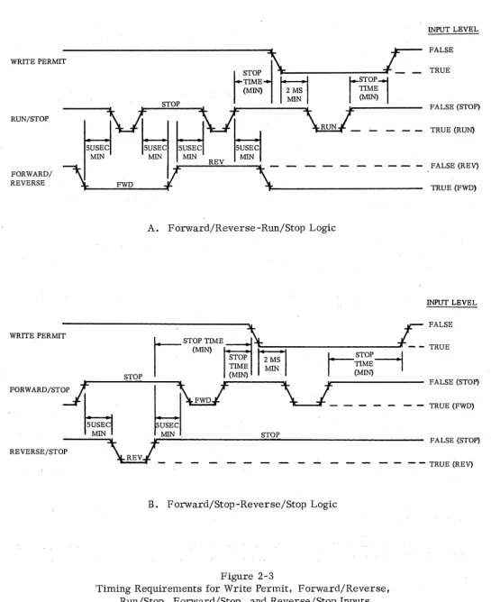
2-13. Write Permit. (See Figure 2-3.) The Write Permit leading (and trailing) edge
transition time shall not exceed 5 Ilsec.
The W rite Permit level shall not be changed while the tape is in motion.
W rite Permit should be at the FALSE level during Reverse and Rewind operations.
2-14. Read Permit. The Read Permit leading (and trailing) edge transition time shall not
WRITE DATA
WRITE STROBE
'90%
1.5 1.5 2.0
USEq USEC USEC
MIN MAX MIN
START
10%
1.5 1.5
SEC USE MAX MIN
INPUT LEVEL
FALSE
TRUE
FALSE
_ _ _ _ TRUE
STOP
_ T,..!ME
(MINl _ _ _ _ _ _ _ _ _ FALSERUN COMMAND*/STOP
.- RUN . COMMAND
TRUE
*
_ Run Command is Run in Fwd/Rev-Run/Stop logic systems and-;' Forward or Reverse in Fwd/Stop-Rev/Stop logic systems.
Figure 2-2
[image:16.620.43.562.49.697.2]2-15. HI/La Density. The HI/La Density leading (and trailing) edge transition time shall be 5 Ilsec maximum. High density is selected by a TRUE level. The high/low density line selects the appropriate timing read circuits.
"NOIE
This signal is normally supplied from the tape transport Operator Control Panel.
2 -16. Odd/Even Parity. The Odd/Even Parity leading (and trailing) edge transition time
shall not exceed 5 Ilsec. Odd parity is selected by a TRUE level. The Odd/Even Parity line is used to select odd or even Read Vertical Parity check.
2 -17. Forward/Reverse. The Forward/Reverse leading (and trailing) edge transition time
shall not exceed 5 Ilsec. (See Figure 2-3A.) The Forward mode is active when this line is at the TRUE level. Forward/Reverse transitions shall not occur while the tape is in motion.
A minimum interval of 5 Ilsec is required between a Forward/Reverse transition
and the Run/Stop transition ~
Write Permit should be at the FALSE level when tape is moving in the Reverse direction.
2-18. Run/Stop. The Run/Stop leading (and trailing) edge transition time shall not exceed
5 Ilsec. (See Figure 2-3B.) A TRUE level on this line sets the transport in the Run mode.
A minimum interval of 5 Ilsec is required between the Forward/Reverse transition and the Run command.
A minimum interval of 2.0 ms is required between a Write Permit transition and a Run command.
INPUT LEVEL
~
sTOP1i\
L
.
t~~
g
t-~~~1
I ;,;;; I
I
(MIN)SWuV~ ~
FALSE WRITE PERMIT
TRUE
RUN/STOP
FALSE (STOP)
TRUE (RUN)
FORWARD/ REVERSE
5USEC
15~;~cl
~
~,._M_IN
_ _ F;;;"W';';';;;'D _ _--"I.v
MIN REV MIN \ _ _ __ _ _ _ _ _ _ - FALSE (REV)TRUE (FWD)
A. Forward/Reverse-Run/Stop Logic
INPUT LEVEL
r-
STOPTIME~~~
_ _~
_ _ _ _ _ _ _ _ _ _~~
::::E(MIN) ~
STOP 2MS
r~~~---J
TIME MIN
I
WRITE PERMIT
STOP (MIN) (MIN)
FORWARD/ST:Arr--..
-I----~--
.
..,.~
\ /-_--_--_-_--_-_-
::::E(~:)O
.. 5USEC USEe
, M I N MIN , STOP
REVERSE/STOP
~. }f~--~---~--- FALSE(STO~
~
- - ' - - - TRUE (REV)B . Forward/Stop - Reverse/Stop Logic
Figure 2-3
[image:18.626.20.566.50.718.2]2-19. Forward/Stop (Option). The Forward/Stop leading (and trailing) edge transition time shall not exceed 5 flsec. (See Figure 2 -3B.) The Forward mode is active when this line is at the TRUE level.
A minimum interval of 2.0 ms is required between a Write Permit transition and a Forward command.
A minimum interval equal to the stop time (to allow tape motion to stop) is required between the 90-percent point of a Stop command transition and a Write Permit transition.
2-20. Reverse/Stop (Option). The Reverse/Stop leading (and trailing) edge transition time
shall not exceed 5 flsec. (See Figure 2-3B.) The Reverse mode is active when this line is at the TRUE level. A minimum interval equal to the stop time (to allow tape motion to stop) is required between the 90-percent point of a stop command transition and a Write Permit tran-sition.
Write Permit should be at the FALSE level when tape is moving in the Reverse direction.
2-21. Rewind. The Rewind leading (and trailing) edge transition time shall not exceed 5
flsec. The Rewind signal shall remain at the TRUE level for at least 5 flsec . Rewind opera-tion is initiated by the negative -going transiopera-tion.
2-22. Rewind and Lockout. The Rewind and Lockout leading (and trailing) edge transition
time shall not exceed 5 flsec. The Rewind and Lockout signal shall remain at the TRUE level for at least 5 flsec. Rewind and lockout operation is initiated by the negative -going transition.
2-23.
2-24.
OUTPUT SIGNAL CHARACTERISTICS.
OUTPUT SIGNAL VOLTAGE AND CURRENT LEVELS.
TRUE Level: -ll.5 (+2.5, -0.5) volts; 5 ma maximum from the load
FALSE Level: 0.00 ±1. 25 volts; 5 ma maximum to the load
NOIE
2-25. OUTPUT SIGNAL TIMING.
In the following description of output signal timing, transition times are measured from the lO-percent point to the percent point. Signal duration is measured from the 90-percent point on the leading edge transition to the lO-90-percent point on the trailing edge tran-sition. Maximum leading edge displacement between Read Data, Read Clock, and Vertical Parity Error outputs is 0.3 I-lsec maximum.
The trailing edge transition times may be affected by the external load circuits.
2-26~ Read Data. The Read Data leading edge transition time is 0.30 I-lsec maximum.
The trailing edge transition time is 0.30 I-lsec. Signal duration is from 0.9 I-lsec minimum
to 1.5 psec maximum.
2 - 27. Read Clock. The Read Clock leading edge transition time is O. 30 I-lsec maximum.
The trailing edge transition time is O. 30 I-lsec .. Signal duration is from O. 9 I-l sec minimum to 1. 5 I-lsec maximum.
2-28. Vertical Parity Error (Option). The Vertical Parity Error leading edge transition
time is O. 30 I-lsec maximum. The trailing edge transition time is O. 30 I-lsec maximum. Signal duration is from O. 9 I-lsec minimum to 1. 5 I-lsec maximum.
2-29. Write Check Error (Option). The Write Check Error leading edge transition time
is 0.30 I-lsec maximum. The trailing edge transition time is 0.30 I-lsec maximum. Signal duration is from 0.5 I-lsec minimum to 5.3 I-lsec maximum.
2-30. Write Enable Status .. Three lines are provided to indicate the state of the write
permit relay on the Data Electronics Write Power Gate PCBA. When a file-protect condition exists, the write permit relay is deenergized and the Write Enable Status (C) line is con-nected.to the Write Enable Status (NC) line. When a write enable condition exists, the write permit relay is energized and the Write Enable Status(C) line is connected to the Write Enable Status (NO) line.
2-31. LP Error (Special Feature). The LP Error leading edge transition time is 0.30 I-lsec
2-32. T APE TRANSPORT STATUS OUTPUTS.
Tape transport status output levels are -1l.5 (+2.5. -0.5) volts (5 ma maximum
from the load) and 0.00 ± 1. 25 volts (5 rna maximum to the load) for TRUE and FALSE.
respectively. unless otherwise indicated. The status outputs are active in the remote mode only.
2-33. Beginning-of-Tape (BOT). A TRUE level on the BOT line indicates that the BOT tab
is being sensed by the photo sense assembly.
2-34. End-of-Tape (EaT). A TRUE level 011 the EaT line indicates that the EaT tab is
being sensed by the photosense assembly.
2-35. High/Low Density Status. The High/Low Density Status line aCknowledges the
density select level. A TRUE level indicates that high density has been selected. A FALSE level indicates that low density has been se,lected.
2-36. Ready. A TRUE level on the Ready line indicates that all tape transport interlocks
are closed and the transport is ready for remote operation.
2-37. Rewinding. A TRUE level on the Rewinding line indicates that the rewind operation
is being performed.
2-38. Unit Select. A TRUE level on the Unit Select line indicates that the tape transport
has been selected by a TRUE level at the Select input (when a single tape transport is used,
the Select line is returned to -12 volts in the Data Electronics, thus providing a TRUE Select
level at all times).
2-39. Select and Remote Indicator. This line is driven by a line driver returned to
INPUT/OUTPUT PANEL CONNECTOR }4 PIN NO.
! e 1 f Z d Y c X W C D E F M N P R S G j k A B H } K L T U V a b g h m
TABLE 2-3
SYSTEM INPUT CONNECTIONS (TYPICAL)
INPUT SIGNAL
Fwd/Rev (or Rev/Stop) Odd/Even Parity
Rewind Command Rewind and Lockout Read Permit
Run/Stop (or Fwd/Stop) Write Permit
Write Reset W rite Strobe Write Track 1
W rite Track 2 Write Track 3 Write Track 4 Write Track 5 W rite Track 6
W rite Track 7 Write Track 8 W rite Track 9
Spare Spare Spare Ground Ground Ground Ground Ground Ground Ground Ground Ground Ground Ground Ground Ground Shield Ground
DATA ELECTRONICS CONNECTOR}5 PIN NO.
INPUT/OUTPUT PANEL CONNECTOR J5 PIN NO.
W X e R C D E F M N P G d Z Y k 1 h c V b a j f A B H
J
K L S T U g illTABLE 2-4
SYSTEM OUTPUT CONNECTIONS (TYPICAL)
OUTPUT SIGNAL
BegiIming-of-Tape End-of-Tape
High/Low Density Status Read Clock
Read Track 1
Read Track 2 Read Track 3 Read Track 4 Read Track 5 Read Track 6
Read Track 7 Read Track 8 Read Track 9 Ready
Rewinding
Unit Select
Select and Remote Indicator Vertical Parity Error* W rite Check Error * Write Enable Status (C)
Write Enable Status (NC) Write Enable Status (NO)
Spare (or LP Error~'*)
Spare Ground Ground Ground Ground Ground Ground Ground Ground Ground Ground Shield Ground
*Spare when option is not supplied.
DATA ELECTRONICS CONNECTOR J4 PIN NO.
TABLE 2-5
DATA ELECTRONICS- TO READ HEAD INTERCONNECTIONS
DATA ELECTRONICS READ HEAD SIGNAL
Jl PIN NO. Jl PIN NO. DESCRIPTION
2 A Read Track 1
12 D Read Track 1
23 H Read Track 2
33 L Read Track 2
4 P Read Track 3
14 T Read Track 3
25 W Read Track 4
35 Z Read Track 4
6 a Read Track 5
16 X Read Track 5
27 U Read Track 6
37 R Read Track 6
8 M Read Track 7
18 J Read Track 7
29 E Read Track 8
39 B Read Track 8
21 C Read Track 9
31 F Read Track 9
9 c Head Ground
22 --* Shield Ground
TABLE 2-6
DATA ELECTRONICS TO WRITE HEAD INTERCONNECTIONS
DATA ELECTRONICS WRITE HEAD SIGNAL
J7 PIN NO. J2 PIN NO. DESCRIPTION
2 A Write Track 1
12 D W rite Track 1
22
--
Shield Ground 123 H W rite Track 2
33 L Write Track 2
13
--
Shield Ground 24 P Write Track 3
14 T Write Track 3
24
--
Shield Ground 325 W Write Track 4
35 Z Write Track 4
15
--
Shield Ground 46 a W rite Track 5
16 X Write Track 5
26
--
Shield Ground 527 U Write Track 6
37 R Write Track 6
17
--
Shield Ground 68 M Write Track 7
18 J Write Track 7
28
--
Shield Ground 729 E Write Track 8
39 B W rite Track 8
19
--
Shield Ground 821 C Write Track 9
31 F W rite Track 9
11
--
Shield Ground 920 b Erase Head Power
30 d Erase Head Return
40
--
Shield Ground Erase Head10 S Write Power (Head CT)
9 c* Head Ground
--
--**
Common Shield*Head ground also terminated at the write head with lug El, which is attached to chassis ground near the write head.
TABLE 2-7
DATA ELECTRONICS TO TAPE TRANSPORT INTERCONNECTIONS
DATA ELECTRONICS SIGNAL TM-7/TM-9
J6 PIN NO. DESCRIPTION J10 PIN NO.
6 Beginning-of-Tape (-) 6
8 End-of-Tape (-) 8
1 Forward/Reverse (- /+)* 1
7 High/Low Density (-/+) 7
19 High/Low Density Status ( - /+) 19
10 Ready (-) 10
4 Rewind and Lockout ( -) 4
3 Rewind Command ( -) 3
9 Rewinding ( -) 9
2 Run/Stop (-/+)** 2
5 Select (-) 5
18 Select and Remote Indicator (+) 18
14 Unit Select (-) 14
15 Write Enable Switch/Relay (C) 15
16 Write Enable Switch/Relay (NC) 16
17*** Write Enable Switch/Relay (NO) 17
11 Ground 11
12 Ground 12
13 Ground 13
20 Shield Ground 20
*Reverse/Stop (-/+) when Fwd/Stop-Rev/Stop logic is supplied. **Forward/Stop (-/+) when Fwd/Stop-Rev/Stop logic is supplied ***.pin 17 of J6 is returned to ground in the Data Electronics
TM-11/TM-12 CONTROL ELECTRONICS
J4 PIN NO.
11 12 14 7 3
2 9 8 1 15
4 6 5 18 17
[image:26.621.28.548.65.742.2]TABLE 2-8
DATA ELECTRONICS TO POWER SUPPLY INTERCONNECTIONS
DATA ELECTRONICS LOGIC POWER SUPPLY
TSI TERMINAL NO. TSI TERMINAL NO. VOLTAGE
1 6 +12 VDC (Regulated)
2 8 Ground
3
.
10 -6 VDC (Regulated)4 12 Ground
5 2 -12 VDC (Regulated)
6 4 Ground
7 13 +24 VDC (Unregulated)
8 14 Ground
9 15 , -24 VDC (Unregulated)
[image:27.615.51.578.124.766.2]3-1. INTRODUCTION.
SECTIDN III
DPERATIDN
This section briefly describes the operation of the Data Electronics.
3-2. OPERATING MODES.
The Data Electronics is capable of operating in three different modes: write check, write only, and read only. The operating mode is determined by the level of the Read Permit and Write Permit input signals.
3-3. WRITE CHECK MODE.
In the Write Check Mode, information is read immediately after it is written. To operate in the Write Check Mode, Write Permit and Read Permit inputs must be TRUE.
3 -4. WRITE ONLY MODE.
In the Write Only Mode, information is written but reading does not occur. To operate in the Write Only Mode, Write Permit input must be TRUE and Read Permit input must be FALSE.
3-5. READ ONLY MODE.
In the Read Only Mode, information is read, but writing does not occur. To operate in the Read Only Mode, Read Permit input must be TRUE and Write Permit input must be FALSE.
3-6. WRITE SIGNAL CONDITIONING.
Writing of data is accomplished on seven (or nine) tracks. In the following
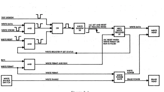
3-7. WRITE DATA. '(See Figure 3-1.)
Data is written when the Write Data input is strobed through an AND gate by the Write Strobe and fed, via an OR gate, to the Write Deskew single-shot delay. Write Head gap-to-gap static skew is compensated for by the single-shot delay. The deskewed Write Data signal is fed to the write register. Write Permit is comprised of the ANDed Write Permit and Run inputs. The write register controls the direction of current flow in the write head.
3 -8. WRITE POWER.
When the Write Permit signal isTRUE and a Write Enable Ring is in place, power is supplied to the Write and Erase Heads through the Write Power Gate.
3 -9. WRITE RESET.
The Write Reset signal is ANDed wi~ the Set status output of the NRZ Write Register
and is theJ:l fed to the NRZ Write Register flip-flops via the OR gate and the single-shot delay. , The Write Reset line is used to write the Longitudinal Check Character (LCC) at the end of , each block of data. The LCe is used to reset the NRZ register, resulting in an even number , of flux reversals (ONEs) in each track of the block.
TEST DESKEW
L.
WRITE DATA
.
l . [
11..
WRITE (AC SET AND RESET IV TRAILING EDGE) WRITE DATA...
WRITE STROBEl.[ •
...
OR DESKEW --"' NRZI'AND
I t . .
-.
55 WRlTE WRITEREGISTER
...
HEAD~ FF t-:- '
l.f ... -
' - ~WRITE RESET
1.f'
(DC RESET WHENWRITE PERMIT OR
AND ,RUN IS FALSE)
r
WRITE REGISTER FF SET STATUSRU"I
AND WRITE PERMIT AND RUN
WRITE PERMIT
...
I
WRITEWRITE PERMIT POWER
r WRITE
POWER
WIIITE WRITE ENABLE
-"' GATE ERASE POWER
.
ERASEEN~,BLE
HEAD SWrrCH
Figure 3-1
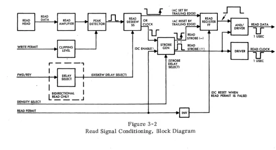
[image:30.620.34.565.397.697.2]3-10. READ SIGNAL CONDITIONING.
Reading of data is accomplished on seven (or nine) tracks. In the following description of read signal conditioning, only one track is discussed.
3-11. READ DATA. (See Figure 3-2.)
The signals from the Read Head are amplified by the Read Amplifier and fed to the peak detector circuit on the Read Deskew PCBA. The peak detector generates positive pulses, corresponding in time to the peaks of the analog Read Head signals. The peak detector clip-ping level is established as a function of W rite Permit.
The Read Data from the peak detector is fed to the Read Deskew single-shot delay. Read head gap-to-gap static skew is compensated for by the single-shot delay. The deskewed Read Data signal is fed to the Read Register. Bi -directional Read Deskew circuits are avail-able as an option.
When a Read Permit signal is present, thc= Read register assembles the deskewed Read Data signals within each character frame and drives the data output drivers.
3-12. STROBE GENERATION.
The Strobe Generator provides the Strobe signal for the Read Data and Read Parity Error AND gates, and the Read Clock signal to the Read Clock output driver.
(AC SET BY
IL--.
TRAILING EDGE)~
READ
READ READ
READ DATA READ
r----+
PEAK DESKEW OR (AC RESET BY REGISTERHEAD AMPLIFIER DETECTOR r
SS CLOCK TRAILING EDGE)--. FF AND/ READ DATA
DRIVER
1..r
1.[
M
READ ~1 USEC STROBE (-)
I I
WRITE PERMIT CLIPPING STROBE
Jl
READ(DCENAB~ GEN STROBE (+) READ CLOCK
LEVel DRIVER
1J
(STROBE 1 USEC
r - - - '
DELAYI
I SelECT)FWD/REV DelAY I (DESKEW DELAY SelECT)
I SELECT I
I
L
I
BIDIRECTIONAL
I
(DC RESET WHENR~O~ _.1 READ PERMIT IS FALSE)
DENSITY SELECT READ PERMIT
INV
Figure 3-2
Read Signal Conditioning, Block Diagram
...
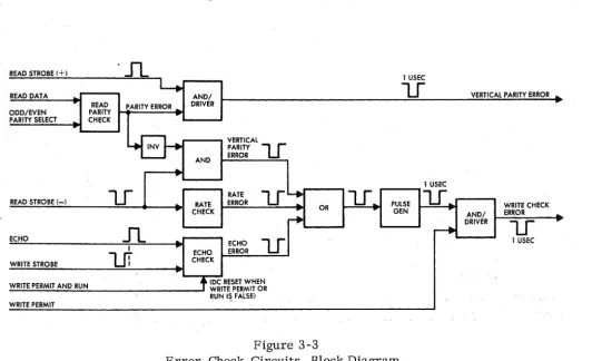
[image:31.618.44.595.450.749.2]3-13. ERROR CHECKING.
3-14.
VERTICAL PARITY CHECK.The vertical parity check circuits generate an Error signal when the parity of the read register does not correspond to the status of the Odd/Even Parity input. In the Read Only Mode, the Error output is provided at the Vertical Parity Error output. In the Write Check Mode, the error indication is provided at the Vertical Parity Error output and at the Write Check Error output
3-15.
RATE CHECK.The rate check circuit generates a Write Check Error output when the time interval between successive characters is below a design threshold. ,
3-16.
ECHO CHECK.In ORed Clock systems, at least one Write Amplifier flip-flop must change state after each Write Strobe. The echo check circuits generate a Write Check Error output when none of the Write Amplifiers change state after receipt of a Write Strobe.
READ STROBE (+)
"11.
4
1 USECREAD DATA AND/
1J
VERTICAL PARITY ERRORREAD PARITY ERROR DRIVER
ODD/EVEN PARITY
PARITY SELECT CHECK
l.B-+
VERTICALPARITY
1J
AND ERROR
1 USEC
1J
RATElS~,
1J ..
1.[
READ STROBE (-) RATE ERROR OR PULSE WRITE CHECK
CHECK
-+
GEN AND/ ERRORDRIVER
1I
~Sl
r+
ECHO --.
ECHO
1J
1 USECI ~
ECHO ERROR
WRITE STROBE
1.IT
CHECK,
WRITE PERMIT AND RUN .,. (DC RESET WHEN WRITE PERMIT OR RUN IS FALSE) WRITE PERMIT
Figure 3-3
[image:32.624.35.567.394.717.2]SECTION IV
THEDRY OF OPERATION
4-1. INTRODUCTION.
This section includes the theory of operation of the data electronics and an intro-duction to the graphic symbols used in the logic diagrams. The theory of operation descrip-tion comprises input/output interface, write logical sequence, read logical sequence, and error check functions.
4-2. LOGIC DIAGRAMS.
The data electronics logic diagrams are located at the end of Section VII. Graphic symbols used in the logic diagrams comply with Military Standard MIL-STD-806B, except that squares and rectangles are used interchangeably for special circuits.
4-3. Logtc Element Identification. Identification of a logic element is accomplished by
the graphic symbol and the notations within and adjacent to the symbol. (See Figure 4-1.) The mnemonic (top) designation within the symbol identifies the printed circuit board (PCB) type. The alphanumeric (bottom) designation within the symbol identifies the physical location of the PCB in the data electronics card cage. Dashed lines indicate internal connec-tions on the PCB. Numbers adjacent to the
logic element indicate the PCB pin number for the connecting signal line.
4-4. State Indicators. A state indicator
(small circle) at the input to any logic element indicates that the relatively-low level of the input signal activates that function of the logic element. A state indi-cator at the output of any logic element indicates that the output level of the acti-vated function is relatively low.
4 -5 . Signal Call outs . Signal callouts
in the data electronics logic diagrams show the TRUE (active) state of the signal.
Write Permit (-) indicates that Write Permit is TRUE when the Write Permit (-) signal is relatively low. Read Strobe (+) indicates
DASHED LINE INDICATES CIRCUIT ON
_PCB} _ _
PCB PIN NUMBER ~22
SOLID LINE INDICATES CIRCUIT EXTERNAL TO PCB
MNEMONIC DESIGNATION OF PCB TYPE
rC
(WRITE AMPLIFIER)CIRCUIT
..----7~ IDENTIFICATION
~~~J
--
~IN~L~SHOT~
AlB '
~
PCB LOCATIONthat Read Strobe is TRUE when the Read Strobe (+) signal is relatively high. Run/Stop (-/+) indicates Run (-) is TRUEwhen the Run/Stop . . . (-/+) signal is relatively low and Stop (+) is TRUE when the signal is relatively high.
4-6. Signal Flow Direction. Direction of signal flow is indicated by logic symbol
orientation. Inputs to a circuit are from the left and outputs are from the right.
Signal flow other than from left to right is indicated by directional arrowheads on the signal lines.
4-7. INPUT/OUTPUT INTERFACE.
4-8. GENERAL.
Most of the signals used in the data electronics logic circuits are binary. Where
binary levels are used, one of the two levels is a 0.0
±O.
5 volt level. The second level isgenerally a -6 volt level. In some circuits, -12 volt, +6 volt, or +12 volt levels are used.
When the binary levels are 0 and -6 or 0 and -12; the 0 volt level is relatively high and is therefore termed positive (+), the -6 volt and -12 volt levels are relatively low and are there-fore termed negative '( -). When the binary levels are 0 and +6 or 0 and +12; the 0 volt level is relatively low and is therefore termed negative (-), the +6 volt and +12 volt levels are relati vel y high and are therefore termed positive (+).
Input buffers are used in the input interface to condition the system input signals to the logic levels required by the data electronics circuits. Output drivers are used in the out-put interface to condition the data electronics outout-put signals to the levels required for the system output signals.
4-9. INPUT BUFFERS (TYPICAL).
The system input line to each input buffer is returned to ground through a line ter-minating resistor. Each system input signal level is compared with a fixed reference voltage in transistor gate circuits on the input buffer PCB. When the level of an input signal exceeds the gate threshold level established by the reference voltage, the output of the input buffer circuit is switched from one binary logic level to the other. When the system input signal level falls below the gate threshold level, the output of the input buffer is switched back to the other binary logic level. The input buffers provide high-noise-immunity inputs for the system.
4-10. OUTPUT DRIVERS (TYPICAL).
The output drivers for the data electronics are located on the output driver PCB· assemblies. NAND gate/drivers are used in each output driver circuit. The NAND gates provide for read strob'e control of the system read data outputs and for inhibit of other' system outputs when required. The NAND gates are enabled by relatively-high level (or open circuit) inputs.
4-11. WRITE LOGIC SEQUENCE.
4-12. WRITE DATA.
A TRUE (low level) Write Data signal at pin 12 of the write amplifier data input AND gate enables the AND gate. A Write Strobe pulse coincidental with the TRUE Write Data signal produces a going pulse at the output of the AND gate. The negative-going pulse is applied through a NOR gate to the input of the Write Deskew single -shot delay. The positive-going pulse from the NOR gate triggers the single-shot delay, which produces
a positive -going pulse. The width of the single -shot delay pulse is adjustable and is set to . compensate for the gap-to-gap misalignment (static skew) of the write heads.
The negative-going trailing edge of the single-shot delay pulse triggers the Write Register flip-flop and the flip-flop changes state. When the flip-flop changes state, the direction of current flow through the write head is reversed, which causes the polarity of the head magnetic flux to reverse. The flux polarity change is impressed on the tape and is interpreted as a logical ONE during the read function.
4-13. WRITE RESET.
The Write Reset signal is used to reset the Write Register flip-flops and to generate
the LPC character. The Write Register flip-flops are in the reset state at the start of each
block of write data. If an odd number of data bits are written on anyone track, that Write
Register flip-flop is in the set state after the last data bit of the block is written. A low level status signal from the set flip-flop enables the Write Amplifier reset AND gate. The Write Reset pulse produces a negative-going pulse at the output of the reset AND gate. The negative-going pulse is applied through the NOR gate to the input of the Write Deskew single-shot delay and causes a ONE to be written as previously described for the Write Data input. The Write Register flip -flop is then in the re set state.
4-14.
WRITE REGISTER DC RESET.The Write Permit signal input is inverted and NANDed with the inverted Run/Stop signal input (or with the inverted Fwd/Stop signal input in Fwd/Stop-Rev/Stop logic systems). The NAND gate is located on the strobe generator PCB. When either the Write Permit signal or the Run/Stop (or Fwd/Stop) signal is at the FALSE (high) level, the output of the NAND gate is at the low level. The low level output from the NAND gate DC resets the Write Register flip-flops and holds the flip-flops in the reset state.
4-15.
TEST DESKEW.A negative-going Test Deskew pulse train applied at test point TP1 of the Data Elec-tronics is applied through the Write Amplifier NOR gates to the inputs of the Write Deskew single-shot delays. The pulses cause all ONEs to be written as previously described for the Write Data input. The Test Deskew input is used during off-line Write Deskew adjustment procedures. The Write Reset and the Write Strobe inputs must be FALSE when the Test Deskew input is used.
4-16.
WRITE HEAD POWER.Write Head Power is furnished by the Write Power Gate. When the Write Permit input is at the TRUE level and a write enable ring is in place in the file reel, +10 volt power is supplied to the write heads from the write power gate PCB through pins 28, 29, and 30. The write power relay on the write power gate PCB is energized when the write enable ring is sensed by the write enable switch assembly on the tape transport.
4-17.
READ LOGICAL SEQUENCE.4-18.
READ PERMIT.Read Permit TRUE enables the read strobe generator circuits. Read Permit FALSE DC resets the read register flip-flops and holds the flip-flops in the reset state.
4-19.
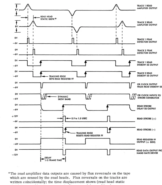
READ DATA. (See Figure 4-2.)!~---~
v
L '
- I
I ~_ READ HEAD -, ~ STATIC SKEW*r : / ; \
.
L
I I1
I
,
I
:V
I IOV I
-6V
~~~----
________________~
n:
1
OV
n
-6V ____ ~~L---~
n
I
_:: I ....
---,._".,f
I1
f
;':\
I I
,
:;':\
I I
I
n
I
n
TRACK 1 READ AMPlifiER OUTPUT
TRACK 2 READ AMPLIFIER OUTPUT
TRACK 1 PEAK DETECTOR OUTPUT
TRACK 2 PEAK DETECTOR OUTPUT
~ TRACK 1 READ
... _ _ ~1 DESKEW SS OUTPUT
OV---~ I • ~---_.
Lt
r---
I
r-
TRACK 2 READ-6V L....J. __ TRAILING EDGE
L-...J
DESKEW SS OUTPUT SETS READ REGISTER FFOV
---.,U
-6V
u
U--OR CLOCK OUTPUT FROM READ DESKEW SS I
OV - - - -... 1
, tI,'_ ....
__
DYNAMIC
-6V l!JJ SKEW BAND
I
\fJ:
I I
J
lff!
OR CLOCK INPUTS TOI
.1
STROBE GENERATOROV
---i
l~~____'f
-6V
I I
\ _____ ---If
L
+12V ~
n
-6V _________ -r-_ _ _ _ _
:=J_.J
I
~ 0.9 to 1.5 USEC '--__________ __ IOV ---1---...;1
-6V
Lf~
TRAILING EDGEl.f
!
RESETS READ REGISTER FF_:: __________
~~---~I~I
I
OV
--:"---U
U
-12V
l...DELAY
.-I
f~1/2 FRAME TIME - ,*The read amplifier data outputs are caused by flux reversals on the tape which are sensed by the read heads. Flux reversals on the tracks are written coincidentally; the time displacement shown (read head static
skew) is caused by gap-to-gap misalignment of the read heads.
Figure 4-2 Read Deskew Timing
READ STROBE DELAY SS OUTPUT
READ STROBE (+)
READ STROBE (-)
READ REGISTER FF OUTPUT (+ SIDE)
[image:37.618.53.580.61.661.2]The differential output from the amplifier on the read deskew PCB assembly is clipped in a clipping stage at the input of the peak detector circuit. The clipping level is established by the clipping bias generated on the strobe generator PCB assembly and is selected by the Write Permit signal. The clipping bias level is higher when Write Permit is TRUE.
The clipped analog Read Data signal is applied to the peak detector circuit which produces a positive-going pulse at the positive or negative peaks of the signal. The leading edge of the peak detector output pulse is coincident with the detected peak. The positive-going pulse triggers the Read Deskew single-shot delay, which produces a negative-positive-going pulse. The width of the single-shot delay pulse is adjustable and is preset to compensate for the gap-to-gap misalignment (static skew) of the read heads. Two pulse widths are set for bidirectional read systems; the forward deskew pulse width is selected when the Forward/ Reverse (or Forward/Stop) input is TRUE, the reverse deskew pulse width is selected when the Forward/Reverse (or Forward/Stop) input is FALSE.
The 'positive-going trailing edge of the single-shot delay pulse sets the Read Register flip-flop and the Read Data output at pin 32 of the read deskew PCB goes to the TRUE (high) level. The Read Data output is applied to one input of a NAND gate driver circuit and enables the NAND gate. A Read Strobe (+) pulse coincidental with the TRUE Read Data signal pro-duces a negative-going pulse at the output of the NAND gate driver. The negative-going pulse is a TRUE Read Data output representing a ONE sensed from the tape.
The Read Register flip-flop is reset by the positive-going trailing edge of the Read Strobe (-) pulse.
4-20.
READ STROBE .. The Read Strobe (+) aI),d Read Strobe (-) pulses are generated on the strobe generator PCB assembly. The positive -going trailing edge of each Read Deskew single -shot delay pulse is coupled through an associated inverter driver stage to produce a negative -going OR Clock pulse •. The OR Clock pulses are applied to one common input of an AND 'gate on the strobe generator PCB . The other input to the AND gate is the Read Permit signal. When Read
Permit is at the TRUE (low) level, the OR Clock pulses are passed through the AND gate.
T~e first ORClock pulse through the AND gate triggers the Read Strobe single-shot delay,
which produces a negative-going pulse. The width of the Single-shot delay pulse is adjust-able and is preset to approximately one-half the character frame time, less the read strobe pulse time. Two single-shot delay pulse widths are preset: one for the high density packing rate, the other for the low density packing rate. Selection of the pulse width is accomplished
by switching circuits on the write power gate PCB. When the HI/LO Density line is at the low
level, the High Density pulse width is selected. When the HI/LO Density line is at the high level, the Low Density pulse width is selected.
pUlse. The pulse width of the Read Strobe (+) pulse is approximately one microsecond. The
Read Strobe (+) pulse is inverted through an inverter stage to produce the Read Strobe (-)
pulse.
4-21. ERROR CHECK OPTIONS.
Error check options consist of Vertical Parity Check, Rate Check, and Echo Check. (See The Data Electronics Logic Diagrams in Section VII. )
4-22. VERTICAL PARITY CHECK.
Vertical Parity is checked during both Read Only and Write Check modes of operation by a continuous frame-by-frame check of the contents of the read register. A parity-select level from the customer selects either odd or even parity check. Odd parity requires an odd
number of logical ONEs be recorded in every ~haracter frame. Even parity requires an even
number of logical ONEs in every character frame. A Vertical Parity Error exists when an extra (or missing) logical ONE is detected.
Numerical values in parenthesis in the following circuit description refer to 9 -track systems. The Odd/Even Parity Select line and the complementary outputs of the Read Register flip-flops are applied to the inputs of the parity checking circuit on the Exclusive OR PCB
assembly. Eight Exclu sive OR gate s are used for 7 -track systems, nine for 9 -track systems. Each gate compares two inputs and produces a high level output when the logic levels of the inputs are dissimilar. Seven (or nine) Read Data (-) lines from the Read Register flip-flops and the Odd/Even Parity Select line are applied to four (or five) of the Exclusive OR gates. The outputs of the four gates are applied in pairs to the following two Exclusive OR gates, the outputs of which are compared by a single gate. The output of the single gate is compared in a final Exclusive OR gate with a fixed low level input (in 9 -track systems, the output of the fifth input Exclusive OR gate is compared with the output of the single gate in the final
Exclu-sive OR gate). The output of the final gate is ANDed with the Read Strobe (+) pulse in a NAND
gate driver. If a vertical parity error is sensed, a negative -going Vertical Parity Error pulse
is produced at the output of the NAND gate driver and is transmitted to the customer via the system output connector.
4-23. RATE CHECK.
Rate Check is performed,only during the Write/Check mode. A Rate error pulse is generated when the interval between successive Read Strobe (-) pulses decreases to
. 1
The Rate Check circuit is located on the error check PCB and operates in the
follow-ing manner. (See Figures
4-3
and4-4.)
T~e Read Strobe (-) pulse triggers single-shotdelay A which produces'a negative-going pulse. The positive-going trailing edge of the single-shot delay A pulse triggers single-single-shot delay B, which produces a negative-going pulse. The next arriving Read Strobe (-) pulse retriggers single-shot delay A and also is ANDed with the
output of single-shot delay B. If the Read Strobe (-) pulse and the output pulse from
single-shot delay B ar:e coincident, a rate error pulse is generated.
4-24.
ECHO CHECK .. An Echo output is generated by each Write amplifier whenever the amplifier changes state andreverses the Write head coil current. The Echo output is a positive-going pulse derived from the induced EMF generated by the Write head inductance when the write head coil current reverses.
In ORed Clock systems, the data that is written must cause at least one head driver to change state in each frame. The Echo output of each Write amplifier is ORed with the Echo outputs of all other Write amplifiers to generate an ORed Echo output. The ORed Echo
output occurs if any Write amplifier changes state during the frame interval. If no ORed
Echo occurs during the frame, a malfunction in the Write circuits is indicated and an Echo error pulse is generated by the Echo Check circuits.
The Echo error pulse is generated in the following manner. (See Figures 4-5 and 4-6.) The Write Strobe triggers the shot delay and the leading edge of the
single-shot delay pulse sets the flip-flop. The Write Strobe holds the AND gate FALSE for the .
strobe duration to prevent any output from the AND gate during the period that the single-shot delay and flip-flop are going TRUE. The AND gate is also held FALSE by the single-shot delay pulse for the duration of its delay. The Echo input must occur sometime after the Write Strobe and within the duration of the single-shot output. The Echo input resets the flip-flop.
If no Echo input occurs, the flip-flop remains set at the end of the single-shot delay pulse
and the output of the AND gate goes TRUE, indicating an Echo Error.
4-25.
WRITE/CHECK ERROR.The Vertical Parity Check output, Rate Check output, and Echo Check output are ORed together. The occurence of any error triggers a pulse generator circuit, which pro-duces a negative-going 1 microsecond error pulse. The error pulse is ANDed with Write
Permit. If the Write Permit is TRUE, a negative-going Write Check Error pulse is
READ STROBE (-)
DELAY
A
DELAY
B
Figure 4-3
AND
r - - -
...
RATE ERROR
Rate Error Check, Block Diagram
READ
---".J
STROBE (-)DELAY A
--,L. ___ ....
DELAY Bu
u
r
ERROR PRODUCED WHENTHIRD READ STROBE (-) PULSE OCCURRED TOO EARLY RATE ________________________________ ~ __
__Jr1L. __________ _
ERROR
[image:41.618.55.557.80.748.2]WRITE STROBE
ECHO
WRITE STROBE
DELAY
FLlP.FLOP
u
AND -""
r
.--DELAY S
FF
ECHO AMP
Figure 4-5
Echo Check, Block Diagram
u
u
I
K~
n
n
--~
...
---~ '-ERROR
. . - - - ERROR. NO ECHO FOR
r - - - -.... I~ SECOND WRITE STROBE
ERROR PULSE
---~
[image:42.621.54.558.61.734.2]5 -1. INTRODUCTION.
SECTION V
MAINTENANCE
This section contains adjustment procedures and troubleshooting techniques for the data electronics. Tape transport maintenance is included in the Tape Transport technical manual.
5-2. TEST EQUIPMENT.
Table 5-1 lists the required test equipment.
.
TABLE 5-1
REQUIRED TEST EQUIPMENT
EQUIPMENT RECOMMENDED TYPE
OR EQUIVALENT
Voltmeter Hewlett-Packard HP 412A
Alignment Master Tape Ampex 750-238
Oscilloscope Tektronix 535
Preamplifier Tektronix CA
Square Wave Generator Hewlett-Packard HP 211
5-3. ADJUSTMENT SCHEDULE.
[image:43.617.51.560.242.547.2]5 -4. ADJUSTMENT PROCEDURES.
Tape transport and power supply adjustments must be verified before data electronics adjustments are made. Due to the interrelationship between circuit functions, data electronics adjustments must be made in the following sequence.
1. Clipping Level
2. Read Deskew
3. Write Check
4. Write Deskew
5. Read Strobe Delay
6. Rate Check Reference Time*·
An insulated blade screwdriver is recommended for making adjustments to prevent accidental shorting of components.
The following preliminary checks should be made before any read deskew, write deskew, or read strobe adjustments are made. Verify that the tape path is clean and free
of any restrictions to tape movement. TM -11 and TM
-12
tape transports only: In newinstallations or where the tape guides have been replaced, ensure that the top flanges (caps)
on the spring-loaded tape guides are in contact with the center sleeves of the guides. If the
attaching screws of the top flanges must be tightened to bring the flanges in contact with the sleeves, a torque driver should be used and the screws tightened to 2.5 to 3.0 inch-pounds of torque.
If adjustments are tobe made off line, use Alternate Adjustment Procedure. (Refer
to paragraph 5 -11. )
5-5. CLIPPING LEVEL.
The bias setting adjustment on the Strobe Generator card determines the clipping level. In the Read Only Mode, the clipping level is set at 20 percent. In the Write Check Mode, the clipping level is set at 40 percent. These percentages refer to the base-to-peak amplitude of the signal into the peak detector.
Step 1: Connect the voltmeter negative lead to pin B8 -32 (clip level output) and
the positive lead to TSI-3 (-6 volt reference).
Step 2:
Step 3:
Step 4:
Step 5:
Step 6:
Step 7:
Step 8:
With power ON, select Remote Mode at the Operator control panel (OCP). When the REMOTE indicator goes ON, the system is ready for operation.
Set the Write Permit input to the TRUE level.
Adjust R 9 (bottom potentiometer) on the strobe generator (SO) PCB at B8 to obtain +1.40 ±O. 05 volts between B8-32 and TSl-3, as indicated on the voltmeter. (See Figure 5-1 for potentiometer location.)
HIGH DENSITY DELAY R13
LOW DENSITY DELAY Rl4
HIGH LEVEL CLIP RIO
LOW LEVEL CLIP R9
Figure 5-1
Clip Level and Strobe Delay Potentiometers
Set the Write Permit input to the FALSE level.
Adjust RIO (second-from-bottom potentiometer) on SO to obtain +0.60 ±0.02 volts between B8-32 and TSl-3, as indicated on the voltmeter.
Repeat Steps 3 through 6 to ensure that the level has not changed. This completes the clipping level adjustment.
5-6. READ DESKEW.
The read deskew adjustment is made using a skew alignment master tape (Ampex No. 750-238). The skew correction is accomplished by setting the delay time of each read deskew single-shot so that the trailing edges of the delay pulses are coincident. A reference track is selected and the trailing edge of the center track (track 5 in 9-track systems, track 4 in 7 -track systems) read deskew delay pulse is aligned with the trailing edge of the selected reference track read deskew delay pulse. The center track is then used as the reference track during the read deskew adjustment. A preliminary read-amplifier-gain check is made to ensure that the read amplifier output signal amplitude is adequate for use during the setting of the read deskew single-shot delay times. Steps 3 through 6 pertain to the preliminary read-amplifier-gain adjustment. Steps 7 through 26 pertain to the read forward deskew adjustment. Steps 27 through 41 pertain to the read reverse deskew adjustment and are applicable to
bidireCtional-read systems only.
Where two potentiometer or test point references