FEATURES
•
Single-chip PC AT -to-SCSI host•
adapter•
•
Low-cost connectivity to multiple SCSI peripherals•
•
S-bit DMA or 16-blt PIOtrans-fers supported
•
•
Average data transfer rates upto 4 megabytes/second
Single-Chip PC AT -to-SCSI
I/O Processor
MEMORY DATA BUS
12S-byte FIFO for data buttering Synchronous and asynchro-nous SCSI devices supported Multitasking driver software available now
Up to eight simultaneous I/O tasks supported
•
•
•
Data Sheet
Rev.
3
May, 1991
BIOS available now 6S-pin PLCC or SO-pin QFP packages
Table of Contents
Section Page
1.0 Overview ... 1-1
20 Pin Information ... 2-1 21 Pin Descriptions ... 2-1
3.0 Register Description ... 3-1 3.1 SCSI Sequence Control (SCSISEQ) ... : ... 3-3 3.2 SCSI Transfer Control 0 (SXFRCTLO) ... 3-4 3.3 SCSI Transfer Control 1 (SXFRCTL1) ... 3-5 3.4 SCSI Signal In (SCSISIGI) ... 3-7 3.5 SCSI Signal Out (SCSISIGO) ... 3-7 3.6 SCSI Rate Control (SCSIRA TE) ... 3-8 3.7 Selection/Reselection ID (SELID) ... 3-9 3.8 SCSI ID (SCSIID) ... 3-9 3.9 SCSI Latched Data (SCSIDAT) ... 3-10 3.10 SCSI Data Bus (SCSIBUS) ... 3-10 3.11 SCSI Transfer Count 2-0 (STCNTO, STCNT1, STCNT2) ... 3-11 3.12 SCSI Interrupt Status 0 (SSTATO) ... ; ... 3-12 3.13 Clear SCSI Interrupts 0 (CLRINTO) ... 3-14 3.14 SCSI Status 1 (SSTAT1) ... 3-15 3.15 Clear SCSI Interrupts 1 (CLRINT1) ... 3-17 3.16 SCSI Status 2 (SST AT2) ... 3-18 3.17 SCSI Status 3 (SSTAT3) ... · ... 3-19 3.18 SCSI Test Control (SCSITEST) ... 3-20 3.19 SCSI Status 4 (SSTAT4) ... 3-21 3.20 Clear SCSI Errors (CLRSERR) ... 3-22 3.21 SCSI Interrupt Mode 0 (SIMODEO) ... ~ ... 3-23 3.22 SCSI Interrupt Mode 1 (SIMODE1) ... : ... 3-24 3.23 DMA Control 0 (DMACNTRLO) ... 3-25 3.24 DMA Control 1 (DMACNTRL1) ... 3-26 3.25 DMA Status (DMASTAT) ... 3-37 3.26 FIFO· Status (FIFOSTAT) ... 3-38 3.27 Data Port (DATAPORTL and DATAPORTH) ... 3-39 3.28 Burst Control (BRSTCNTRL) ... 3-30 3.29 Port A (PORT A) ... 3-30 3.30 Port B (PORT B) ... 3-30 3.31 Revision (REV) ... 3-30 3.32 Stack (STACK) ... 3-31 3.33 Test Register (TEST) ... 3-31
4.0 Functional Information ... 4-1 4.1 General Functional Description ... 4-1 4.1.1 SCSI Controller ... 4-2 4.1.2 SCSI Interrupts ... 4-2 4.1.3 SCSI Selection/Reselection Autoconnect Sequencer ... 4-2 4.1.4 SCSI FIFO ... 4-2 4.1.5 Address Mapping and External Decode ... 4-2 4.1.6 Stack ... 4-3 4.1.7 Host Interface, ... 4-3 4.1.8 Host FIFO ... : ... 4-3 4.2 SCSI Data Transfers ... 4-3 4.2.1 SCSI Manual PIa Mode ... ~ .... 4-4 4.2.2 SCSI Automatic PIa Mode ... 4-4 4.2.3 SCSI Normal Mode ... 4-4 4.3 Host Processor Data Transfers ... 4-4 4.3.1 Host PIa Mode ... 4-4 4.3.2 Host DMA Mode ... 4-5 4.4 Interrupts ... 4-5 4.5 External PortsDecode ... 4-6 4.6 Clocking ... 4-6 4.7 Power Management ... 4-7 4.7.1 Powerdown-Sleep Mode ... 4-7 4.8 Testing ... 4-7
Table of Contents
6.0 Electrical Information ... 6-1 6.1 Absolute Maximum Ratings ... 6-1· 6.2 Operating Conditions ... ~ ... 6-1 6.3 DC Electrical Characteristics ... 6-1 6.4 System Timing ... 6-2 6.4.1 Host Processor PIO Data Read Operation ... 6-2 6.4.2 Host Processor PIO Data Write Operation ... 6-3 6.4.3 Host Processor I/O Read Operation ... 6-4
6.4.4 Host Processor I/O Write Operation ... 6-5 6.4.5 Host Processor DMA Read Operation ... 6-6 6.4.6 Host Processor DMA Write Operation ... 6-7 6.5 SCSI Bus Timing ... 6-8 6.5.1 Arbitration/Selection ... 6-8 6.5.2 SCSI Bus Free Detection ... 6-9 6.5.3 SCSI PIO ... 6-10 6.5.4 SCSI Data Setup and Hold. Latched Data and PIO ... 6-11
7.0 Package Outlines ... 7-1 7.1 68-Pin PLCC ... 7-1 7.2 80-Pin Quad Flatpack ... 7-2
Appendix A: Data Transfer Rate Calculations ... A-l A.l Burst Rate. ... ... ... ... ... ... .... ... .... ... A-l A.2 PIO Transfer Rate Calculation ... A-2 A.3 PIO Transfer Rate Examples ... A-2
Appendix B: Example PIO Transfer Loop ... B-1
Appendix C: PC AT DMA Setup ... C-l
Appendix D: PC AT Interrupt ... D-l D.l Interrupt Initialization ... D-l
D2 Interrupt Response ... D-l
List of Figures
1-1 AIC-6260 Functional Block Diagram ... 1-2 2-1 AIC-6260 Pin Locations ... 2-1 4-1 AIC-6260 Simplified Block Diagram ... 4-1 4-2 Typical External Logic Circuit ... 4-5 5-1 Sample AIC-6260 Application Drawing ... 5-11
List of Tables
2-1 AIC-6260 Pin Descriptions ... 2-2 3-1 AIC-6260 Register Address Map ... 3-1 3-2 STIMESEL Values ... 3-5 3-3 SXFR Codes ... 3-9 3-4 STCTEST Transfer Count Read Register (bits 0-5). To Select Abort
Section One
Overview
The AIC-6260 is a single-chip SCSI solution for PC AT and microprocessor-controlled peripherals applications. The AIC-6260 provides all of the functionality necessary to implement a multiple-unit SCSI in one 6S-pin PLCC or SO-pin QFP package. Typical applications include laptops, portables, and low-end desktop computers.
The AIC-6260 is a single-chip PC AT bus to SCSI bus controller, designed to bring the power and connectivity of SCSI to the computer system motherboard.
The power of SCSI is demonstrated by a sustained d.ata transfer capability of up to 4 megabytes per second. SCSI bus connectivity gives the system the ability to hook up to any of the growing number of SCSI compatible peripherals available, from hard drives to high-capacity floppy drives, tape drives, CD-ROM, DA T and removable drives.
Embedding the AIC-6260 increases reliability, reduces cost and eliminates the need for a traditional host adapter card. This makes the chip an ideal I/O solution for both desktop and laptop systems.
The AIC-6260 supports second party DMA transfers or programmed I/O. The chip contains a 12S-byte data buffer to increase PIO performance. Synchronous or Asynchronous SCSI transfer is supported A built-in "sleep" mode saves power.
Adaptec cuts the system designer's job in half by supporting the AIC-6260 with a full complement of SCSI driver software.
The ASW-1210 is a multitasking ASPI (Advanced SCSI Programming Interface) manager for DOS, and contains features such as DisconnectlReconnect on the SCSI bus. This frees the host CPU while peripherals execute time-consuming functions such as Seeks. Up to eight simultane-ous I/O tasks can be run in the background, and the driver also allows interrupts from the host CPU. Automatic Request Sense can be done in the event of a "Check Condition" status from a SCSI target LUN. This ensures that valuable status data is not lost.
Configuration Options are programmable and can be set by software during system power up. No need for jumpers!
Configurable options are:
• EnableIDisable Disconnect • AT Bus ON/OFF Time • Selection Time Out • Parity Checking Disable • DMA/PIO
• SCSI ID
• Synchronous Negotiation
BIOS code is available to allow booting from the SCSI hard drive and to emulate DOS hard disk calls.
Compatibility is assured by support of the ANSI Common Command Set and SCSI-2.
HOST BUS
OFF CHIP
~
I
EXTRNLI
CNTRL16-BYTE DECODE SCSI
-
..
~
STACK
,
CNTRL ~..
CNTRL..
HOST BUS SCSI
~.
. / ADDR INTERFACE.
-
INTERRUPTS INTRPT~DECODE.
/' 10 AND CNTRL
..
~
~ CNTRL SCSI
SEL/RES
AUTO-..
CONNECT CNTRL SQENCER-~
/HOST BUS
128-BYTE SCSI
r---_ DATAl'" FIFO / ' 8-BYTE
_DATA/ ..
/ 16 /' 8 FIFO , 8
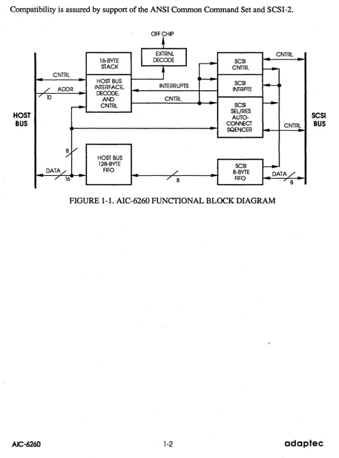
FIGURE 1- L AIC-6260 FUNCTIONAL BLOCK DIAGRAM
[image:7.615.57.553.100.770.2]Section Two
Pin Information
2.1 PIN DESCRIPTIONS
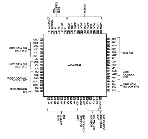
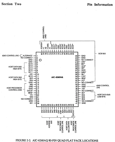
The AIC-6260 is available in a pin PLCC or 80-pin Quad Flat Pack. Figure 2-1 shows the 68-pin PLCC 68-pinout while Figure 2-2 shows the 80-68-pin QFP. Table 2-1 defines the 68-pin assignments for the AIC-6260.
All SCSI lines utilize open collector drivers (I0L=48mA, input hysteresis=.2V).
GNO 1
.
{~~~:
12HOST DATA BUS S013 HIGH BYTE S012
SOll +5V 1
HOST DATA BUS S09 18 {
SOlO
HIGH BYTE S08
{
~:~
HOST PROC ESSOR GNO
CONTROL LINES OACK* SBHE*
HOST ADDRESS T/C BUS -C SAO
AlC-6260AL
~
,-~(f)oo:tlt)o()r-.CIO()'. 3 : Z 0 ... N ( f ) .
~~~~~~~~~QQ~QQQQ~
L - - - r - _ - - - - II
y
II~
~~e/) ~O::e/) ~~ ~o::w
Ow;::)
~~~
OO~o::m C§m I~-J
I e w-J
~~ w-J
e Uo uO
<C 00:: 09 00:: o::z
a:~ Ie/) :::> m 0..0
U U
GNO
MSG*
C/O*
REQ*
51 1/0*
SCSI BUS
50 GNO 6260
MRST
=r
CONTROL+5V LINE
47
~~
} HOST DATA [image:8.613.65.548.246.699.2]SD5 BUS LOW BYTE SD4
FIGURE 2-1. AIC-6260AL 68-PIN PLeC LOCA nONS
6260 CONTROL UNE--c ALTERNATE* NO CONNECT GND
HOST DATA BUS {
im~
HIGH BYTE SD 13SD12 SDll +5V HOST DATA BUS { SD10 HIGH BYTE SD9 SD8
HOST PROCESSOR {
~
CONTROL UNES DACK*SBHE* T/C SAO NO CONNECT GND SAl 1 2
30
4 5 6 7 8 9 10g
AIC-6260AQ 13 14 15 16 17 18 19 20 21 22 23 24~<~ ~::e cncncncncncncn(/)_Qct.cncncncn~
<
~~Q:O~ ~8o S8 ~L..---.-_---"y'
,~
64 63 62 61 60 59 58 57 56 55 54 53 52 51 50 49 48 47 46 45 44 43 42 41 GND GND NO CONNECT ATN* BSV* ACK* RST* GND MSG* SEL* C/D* REQ* 1/0*
SCSI BUS
NO CONNECT GND
MRST - - - 6260 CONTROL +5V UNE
NO CONNECT
~g~
}
HOST DATA BUS SD5 LOWBYlE SD4 [image:9.615.63.554.27.635.2]NO CONNECT GND
Section Two
Pin Information
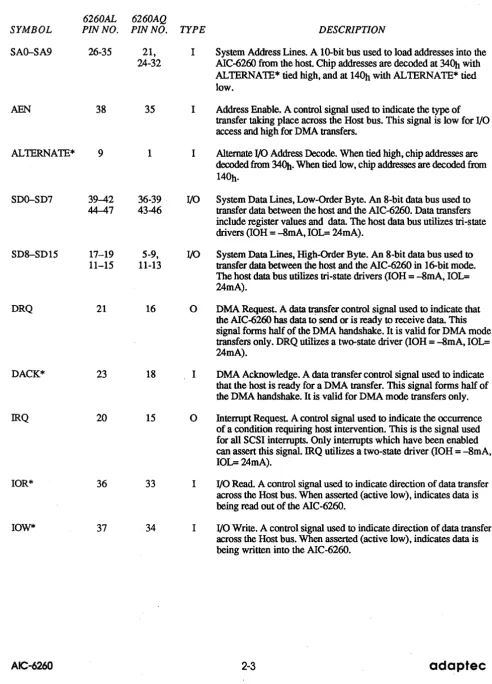
TABLE 2·1. AIC·6260 PIN DESCRIPTIONS
6260AL 6260AQ
SYMBOL PINNa. PINNa. TYPE DESCRIPTION
SAO-SA9 26-35 21, I System Address Lines. A 100bit bus used to load addresses into the 24-32 AIC-6260 from the host. Chip addresses are decoded at 34Db with
ALTERNA1E* tied high, and at 140h with AL1ERNATE* tied low.
AEN 38 35 I Address Enable. A control signal used to indicate the type of transfer taking place across the Host bus. This signal is low for I/O access and high for DMA transfers.
ALTERNATE* 9 1 I Alternate I/O Address Decode. When tied high, chip addresses are
decoded from 34Db. When tied low, chip addresses are decoded from 140h·
SDO-SD7 39-42 36-39 . I/O System Data Lines, Low-Order Byte. An 8-bit data bus used to 44--47 43-46 transfer data between the host and the AIC-6260. Data transfers
include register values and data. The host data bus utilizes tri-state drivers (lOH
=
-SmA, 10L= 24mA).SD8-SDI5 17-19 5-9, I/O System Data Lines, High":Order Byte. An 8-bit data bus used to 11-15 11-13 transfer data between the host and the AIC-6260 in 16-bit mode.
The host data bus utilizes tri-state drivers (lOH
=
-SmA, 10L= 24mA).DRQ 21 16 0 DMA Request. A data t.qmsfer control signal used to indicate that the AIC-6260 has data to send or is ready to receive data. This signal forms half of the DMA handshake. It is valid for DMA mode transfers only. DRQ utilizes a two-state driver (lOH
=
-SmA, 10L= 24mA).DACK* 23 18 I DMA Acknowledge. A data transfer control signal used to indicate that the host is ready for a DMA transfer. This signal forms half of the DMA handshake. It is valid for DMA mode transfers only.
IRQ 20 15 0 Interrupt Request A control signal used to indicate the occurrence of a condition requiring host intervention. This is the signal used for all SCSI interrupts. Only interrupts which have been enabled can assert this signal. IRQ utilizes a two-state driver (IOH
=
-SmA, 10L=24mA).IOR* 36 33 I I/O Read. A control signal used to indicate direction of data transfer across the Host bus. When asserted (active low), indicates data is being read out of the AIC-6260.
10W* 37 34 I I/O Write. A control signal used to indicate direction of data transfer across the Host bus. When asserted (active low), indicates data is being written into the AIC-6260.
[image:10.617.57.550.84.769.2]TIC 25 20 I Terminal Count. A control signal used to indicate the completion of a DMA transfer. This signal is driven by the host DMA controller.
SBHE* 24 19 I
System Bus High Enable. This signal indicates that data on the SD8-SD 15 lines is valid ..
IOCSI6* 43 40 0 I/O Chip Select 16. This signal is driven low when the current I/O data transfer is 16 bits (one word) wide. Open collector driver, 10L =24 rnA.
MRST 49 49 I
Master Reset A control signal is used to restore the AIC-6260 to its start-up condition. This signal is active high at power up or hard reset. This signal has hysteresis for noise immunity. (1.5V <Vth+ <2.0V; .6V <Vth - <1.1V; Vth + - Vth - = AV)
SCDO-7* 1-3 66,67 I/O SCSI Data Bus. An 8-bit data bus used to transfer data between the 62, 69-71, AIC-6260 and devices on the SCSI Bus. Data transfers include 63, 73-75 SCSI commands, Status, Messages and user data. Open collector
65~7 driver, IOL = 48mA, input hysteresis .2V.
SCDP* 61 65 I/O SCSI Data Parity. A control signal used to check for data transfer ·errors on the SCSI bus. This signal with SCSI. data always
generates odd parity when the AIC-6260 is driving the SCSI Bus. This signal is tested when the AIC-6260 is receiving and parity checking is enabled. Open collector driver, 10L = 48mA, input hysteresis .2V.
RST* 57 58 I/O SCSI Reset A control signal used to restore devices attached to the SCSI bus to their start-up condition. This signal is driven under programmed control. When detected, RST* may cause the assertion of IRQ. Open collector driver, IOL = 48mA, input hysteresis .2V.
ATN* 60 61 I/O SCSI Attention. A control signal used to indicate that an initiator wishes to send a Message out to a Target. A TN* is driven when the AIC-6260 is in initiator mode and detected when the AIC-6260 is
in target mode. Open collector driver, 10L = 48mA, input hysteresis .2V.
BSY* 59 60 I/O SCSI Busy. A control signal used for bus arbitration and device selection on the SCSI bus. Open collector driver, IOL = 48 rnA,
input hysteresis .2V. .
SEL* 54 55 I/O SCSI Select A control signal used for device selection on the SCSI Bus. Open collector driver, 10L = 48mA, input hysteresis .2V.
Section Two
Pin Information
I/O* 51 52 I/O SCSI Input/Output. A control signal driven by the target to indicate the direction of transfer across the SCSI bus (SCDO-7 and SCDP). When driven low, indicates data is being passed from the target to the initiator. When driven high, indicates data is being passed to the target from the initiator. 1/0* is driven when the AIC-6260 is in target mode and is detected when the AIC-AIC-6260 is in initiator mode. Open collector driver, IOL
=
48 rnA, inputhysteresis .2V. '
MSG* 55 56 I/O SCSI Message. A control signal driven by the target to indicate the
type of transfer across the SCSI Bus (SCDO-7* and SCDP).
MSG* is driven when the AIC-6260 is in target mode and is detected when the AIC-6260 is in initiator mode. Open collector driver, IOL
=
48mA, input hysteresis .2V.REQ* 52 53 I/O SCSI Request A data transfer control signal used to indicate that the target has data to send or is ready to receive data. This signal forms half of the SCSI data transfer handshake. REQ* is driven when the 6260 is in target mode and is detected when the AIC-6260 is in initiator mode. Open collector driver, IOL
=
48mA, input hysteresis .2V.ACK* 58 59 I/O SCSI Acknowledge. A data transfer control signal used to indicate that the initiator has sent or received data. This signal forms half of the SCSI data transfer handshake. ACK* is driven when the AIC-6260 is in initiator mode and is detected when it is in target mode. Open collector driver, IOL
=
48mA, input hysteresis .2V.PORTEN* 8 80 0 Port Enable. This is an address decode for an external port driver. Address bits 1-9 are included in this signal decode along with AEN. Address bit 0 must be decoded externally with lOR and lOW. (Two-state driver: IOH
=
-2 rnA, IOL=
2 rnA.)+5V 16,48 10,48 I 5-Volt Power Supply. ±5% max. variation. Two pins.
GND 10,22, 3,4,14, I Ground. Six pins. 50,56, 17,23,41,
64,68 50,57,63, 64,68,72
Xl 4 76 I Crystal Input 20 MHz crystal input for internal· oscillator.
X2 6 78 0 Crystal Output 20 MHz crystal output for internal oscillator.
Fl 7 79 I/O Clock In/Out. This pin is either a clock input or output, depending on the condition of CLKSEL. If CLKSEL is tied high, it is a clock output. If CLKSEL is left to float, it is the clock input for the AIC-6260.
CLKSEL 5 77 I Clock Select This pin selects the clock source. If tied to +5 VDC, the internal oscillator circuit is selected as the clock. In this case, CLKSEL provides V dd for the internal oscillator. If left to float, CLKSEL is internally pulled down thereby selecting PI as the clock source.
This section contains infonnation on the AIC-6260' s internal registers. Each register is described under its own heading, identified by name and address.
There are 32 registers, nonnally decoded from 340h through 35Eh. If AL TERNA TE* is asserted (low), the registers are decoded from 140h. Registers are written and read by the host processor via the host bus, in I/O address space.
The following conventions are used throughout this section:
• set:
Indicates that the target bit was loaded with a 1. • clear: Indicates that the target bit was loaded with a O.• (0): Indicates that the associated bit is set to 0 after a hard reset.
• (1): Indicates that the associated bit is set to 1 after a hard reset. • (x): Indicates the state of the bit after a hard reset is undefined.
Table 3-1 is an address map of the AIC-6260 registers.
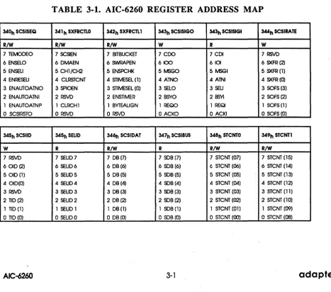
TABLE 3-1. AIC-6260 REGISTER ADDRESS MAP
340h SCSISEQ 341 h SXFRCTLO 342h SXFRCTL 1 343h SCSISIGO 343h SCSISlGl 344h SCSIRATE
R/W R/W R/W W R W
7 TEMODEO 7 SCSIEN 7 BITBUCKET 7 COO 7 COl 7 RSVD 6 ENSELO 6DMAEN 6 SWRAPEN 6100 6101 6 SXFR (2)
5 EN SEll 5 CH1/CH2 5 ENSPCHK 5 tv1SGO 5 MSGI 5 SXFR (1)
4 ENRESELI 4 CLRSTCNT 4 STIMESEl (1) 4 ATNO 4 ATNI 4 SXFR (0) 3 ENAUTOATNO 3 SPIOEN 3 STIMESEl (0) 3 SELO 3 SEll 3 SOFS (3) 2 ENAUTOATNI 2 RSVD 2 ENSTIMER 2 BSYO 2 BSYI 2 SOFS (2) 1 ENAUTOATNP 1 CLRCH1 1 BYTEAUGN 1 REQO 1 REQI 1 SOFS (1)
a SCSIRSTO a RSVD a RSVD a ACKO a ACKI a SOFS(O)
345h SCSIID 345h SELID 346h SCSIDAT 347h SCSIBUS 348h STCNTO 349h STCNTl
W R R/W R R/W R/W
[image:13.615.65.533.362.774.2]Section Three
Register Description
34.AJ, -STCNT2 34Bh CLRSINTO 34Bh SSTATO 34Ch CLRSINTl 34Ch SSTATl 34Dh SSTAT2
R/W W R W R R
7 STCNT (23) 7 SETSDONE 7 TARGET 7 CLRSELTIMO 7 SELlO 7 RSVD 6 STCNT (22) 6 CLRSELDO 6 SELDO 6 CLRATNO 6 ATNTARG 6 RSVD
'-5 STCNT (21) 5 CLRSELDI 5 SELDI 5 CLRSCSIRSTI 5 SCSIRSTI 5 SOFFSET 4 STCNT (20) 4 CLRSELINGO 4 SEUNGO 4 RSVD 4 PHASEMIS 4 SEMPTY 3 STCNT (19) 3 CLRSWRAP 3 SWRAP 3 CLRBUSFREE 3 BUSFREE 3 SFULL 2 STCNT (18) 2 CLRSDONE 2 SDONE 2 CLRSCSIPERR 2 SCSiPERR 2 SFCNT(2) 1 STCNT (17) 1 CLRSPIORDY 1 SPIORDY 1 CLRPHASECHG 1 PHASECHG 1 SFCNT (1) o STCNT (16) o CLRDMADONE o DMADONE o CLRREQINIT o REQINIT o SFCNT (0)
34Eh SCSITEST 34Eh SSTAT3 34Fh CLRSERR 34Fh SSTAT4 350h SIMODEO 351 h SIMODEl
W R W R R/W R/W
7 RSVD 7 SCSICNT (3) 7 RSVD 7 RSVD 7 RSVD 7 ENSELTIMO 6 RSVD 6 SCSlCNT (2) 6 RSVD 6 RSVD 6 ENSELDO 6 ENATNTARG 5 RSVD 5 SCSlCNT (1) 5 RSVD 5 RSVD 5 ENSELDI 5 ENSCSIRST 4 RSVD 4 SCSlCNT (0) 4 RSVD 4 RSVD 4 ENSELINGO 4 ENPHASEMIS 3 SCTESTU 3 OFFCNT (3) 3 RSVD 3 RSVD 3 ENSWRAP 3 ENBUSFREE 2 SCTESTD 2 OFFCNT (2) 2 CLRSYNCERR 2 SYNCERR 2 ENSDONE 2 ENSCSIPERR 1 RSVD 1 OFFCNT (1) lCLRFWERR 1 FWERR 1- ENSPIORDY 1 ENPHASECHG o STCTEST o OFFCNT (0) o CLRFRERR o FRERR o ENDMADONE o ENREQINIT
352h DMACNTRLO 353h DMACNTRL 1 354h DMASTAT 355h FIFOSTAT 356h DATAPORTL 356h DATAPORTH
R/W R/W R R R/W R/W
7 ENDMA 7 PVVRDWN 7 ATDONE 7FCNT(7) 7 DATAL (07) 15 DATAH (15) 6 8BIT 1-16BIT 6 RSVD 6 WORDRDY 6 FCNT (6) 6 DATAL (06) 14 DATAH (14) 5DMA/-PIO 5 RSVD 5 INTSTAT 5 FCNT (5) 5 DATAL (OS) 13 DATAH (13) 4 RSVD 4 RSVD 4 DFIFOFULL 4 FCNT (4) 4 DATAL (04) 12 DATAH (12) 3 WRITE/-READ 3 STK (3) 3DFlFOEMP 3 FCNT (3) 3 DATAL (03) 11 DATAH (11) 21NTEN 2 STK (2) 2 RSVD 2 FCNT (2) 2 DATAL (02) 10 DATAH (10) 1 RSTFIFO 1 STK (1) 1 RSVD 1 FCNT (1) 1 DATAL (01) 9 DATAH (09)
O~NT o STK (0) o RSVD o FCNT (0) o DATAL (00) 8 DATAH (08)
358h BRSTCNTRL 35A PORTA 35B PORTB 35ChREV 35DhSTACK 35Eh TEST
W R/W R/W R R/W w
7 BON (3) 7 PADAT (7) 7 PBDAT (7) 7 RSVD 7 STKDAT (7) 7 RSVD 6 BON (2) 6 PADAT (6) 6 PBDAT (6) 6 RSVD 6 STKDAT (6) 6 BOFFTMR 5 BON (1) 5 PADAT (5) 5 PBDAT (5) 5 RSVD 5 STKDAT (5) 5 BONTMR 4 BON (0) 4 PADAT (4) 4 PBDAT (4) 4 RSVD 4 STKDAT (4) 4 STCNTH 3 BOFF (3) 3 PADAT (3) 3 PBDAT (3) 3 RSVD 3 STKDAT (3) 3 STCNTM 2 BOFF (2) 2 PADAT (2) 2 PBDAT (2) 2 REV (2) 2 STKDAT (2) 2 STCNTL 1 BOFF (1) 1 PADAT (1) 1 PBDAT (1) 1 REV (1) 1 STKDAT (1) 1 SCSlBLK o BOFF (0) o PADAT (0) o PBDAT (0) o REV(Ol o STKDAT (0) o DMABLK
3.1 SCSI SEQUENCE CONTROL (SCSISEQ)
Register Type: RJW
Register Address: 340h
This register controls the Selection/Reselection process for the AIC-6260. Each bit in this register enables a different portion of the SelectionlReselection process. This register can be read, allowing bit manipulation instructions without saving a register image in local scratch RAM. All bits, except SCSIRSTO (bit 0), are cleared by a SCSI Reset.
BIt Field Name
7 TEMODEO
6 ENSELO
5 ENSELI
4 EN RESEll
3 ENAUTOATNO
2 ENAUTOATNI 1 ENAUTOATNP
0 SCSI RSTO
7
(0)
TEMODEO: TARGET Enable Mode Out. TEMODEO is used in conjunction with ENSELO (bit 6). If TEMODEO is set, setting ENSELO initiates a Reselection Out se-quence. If TEMODEO is cleared, setting ENSELO initiates a Selection Out sequence.6 (0) ENSELO: Enable Selection Out. When ENSELO is set, the AIC-6260's SCSI logic performs either a Selection Out, or a Reselection Out, based on the state of TEMODEO. ENSELO is cleared by the processor or by a hard reset of the host.
S
(0)
ENSELI: Enable Selection In. When ENSELI is set, it allows the AIC-6260 to respond to valid Selection In attempts.4 (0) ENRESELI: Enable Reselection In. When ENRESELI is set, it allows the AIC-6260 to respond to valid Reselection In attempts. ENRESELI is reset by clearing it.
3
(0)
ENAUTOATNO: Enable Auto Attention Out. When ENAUTOATNO is set, ATN is asserted during a Selection Out sequence (ENSELO=l, TEMODEO=O). This procedure is used when the AIC-6260 is the initiator and wants to follow Selection with aMessage Out Phase. The processor can deassert A TN by setting CLRA TNO (bit 6, 34Ch, W). A Bus Free state on the SCSI bus also deasserts ATN. Clearing
ENAUTOA TNO does not deassert ATN.
2 (0) ENAUTOATNI: Enable Auto Attention In. With ENAUTOATNI set, ATN is asserted during a Reselection In sequence (ENRESELI=l). This procedure is used when the AIC-6260 is the initiator and wants to follow reselection with a Message Out phase. The processor can deassert A TN by setting CLRA TNO (bit 6, 34Ch, W). A Bus Free state on the SCSI bus also deasserts A TN. Clearing ENA UTOA TNI does not deassert A TN.
1 (0) ENAUTOATNP: Enable Auto Attention Parity. When both ENAUTOATNP and ENSPCHK (bit 5, 342h) are set, A TN is asserted if a parity error is detected on SCQ-SC7 during the Data In, Message In, or Status In phases. The processor can deassert A TN by setting CLRA TNO (bit 6, 34Ch, W). A Bus Free state on the SCSI bus also deasserts A TN. Clearing ENAUTOATNP does not deassert A TN.
Section Three
Register Description
3.2 SCSI TRANSFER CONTROL 0 (SXFRCTLO) Register Type:
RIW
Register Address: 341 h
SCSI Transfer Control 0 to enables transfers between the SCSI bus and the host, via the SCSI and host FIFOs. "This register also controls the selection of SCSI PIO mode as the transfer mode and enables the SCSI FIFO and SCSI transfer counter to clear.
Bit Field Name
7 SCSI EN
6 DMAEN 5 CH1/CH2
4 CLRSTCNT
3 SPIOEN 2 " RSVD. 1 CLRCHl
0 RSVD.
7 (0) SCSIEN: Transfer Enable. When SCSIEN is set, data can be transferred between the SCSI bus and the SCSI FIFO. Transfers are tenninated by clearing SCSIEN. SCSIEN must be read back as a low before the transfer is considered halted. Synchronous data transfers are enabled whenever SOFS (bits 3-0, 344h) is non-zero.
6 (0) DMAEN: FIFO Transfer Enable. When DMAEN is set, transfers between the SCSI FIFO and host FIFO are enabled.
5 (x) CHI/CH2: Channel Select. CH1/CH2 should always be set.
4 (0) CLRSTCNT: Clear SCSI Transfer Counter. When CLRSTCNT is set, the SCSI transfer count (SCXFRCNT, 348h-34Ah) is set to OOOOOOh. The AIC-6260 generates a clear pulse, making it necessary to reset CLRSTCNT. CLRSTCNT is always read back as O.
3 (0) SPIOEN: SCSI PIO Enable. When SPIOEN is set, SCSI PIO mode is used as the transfer mode. Once a SCSI PIO transfer is started, SPIOEN must remain set
throughout the entire transfer. If SPIOEN is cleared at anytime during the transfer, the transfer will be halted without corrupting valid data in the data latch at 346h.
2 (0) RSVD: RSVD. This bit always reads as O.
1 (x) CLRCHl: Clear Channell. When CLRCHI is set, the AIC-6260 generates a pulse to clear the SCSI FIFO, (bits 3-0 of 34Eh), and the SCSI transfer count (348h-34Ah).
0 (0) RSVD: RSVD. This bit always reads as O.
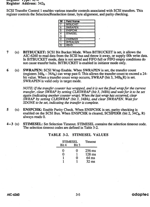
3.3 SCSI TRANSFER CONTROL 1 (SXFRCTLl) Register Type:
RIW
Register Address: 342h
SCSI Transfer Control 1 enables various transfer controls associated with SCSI transfers. This register controls the SelectionlReselection timer, byte alignment, and parity checking.
Bit Field Name
7 BITBUCKET
6 SWRAPEN
5 ENSPCHK
4 STIMESEL
3
2 ENSTIMER 1 BYTEALIGN
0 RSVD.
7 (x) BITBUCKET: SCSI Bit Bucket Mode. When BITBUCKET is set, it allows the AIC-6260 to read data from the SCSI bus and throw it away, or supply OOh write data.
In BITBUCKET mode, data is not saved and FIFO full or FIFO empty conditions do not cause transfer halts. BITBUCKETis enabled in initiator mode only. .
6 (x) SWRAPEN: SCSI Wrap Enable. When SWRAPEN is set, the transfer count (registers 348h - 34Ah) can wrap past O. This allows the transfer count to exceed a 24-bit value. When a transfer count wrap occurrs, SWRAP (24-bit 3, 34Bh,R) is set.
. SWRAPEN is valid only in target mode.
NOTE: If the transfer counter has wrapped, and it is not the final wrap for the current transfer, clear SWRAP by setting CLRSWRAP (bit 3, 34Bh) and wait for it to be set again (indicating another counter wrap). When the last wrap has occurred, clear SWRAP by setting CLRSWRAP (bit 3, 34Bh), and clear SWRAPEN. Waitfor SDONE to be set, indicating the transfer is complete.
S (x) ENSPCHK: Enable Parity Check. When ENSPCHK is set, parity checking is enabled on the SCSI Bus. When ENSPCHK is cleared, SCSIPERR (bit 2, 34Ch, R) always reads O.
4 - 3 (x) STIMESEL: Set Selection Timeout. STIMESEL contains the selection timeout code. The selection timeout codes are defined in Table 3-2.
TABLE 3-2. STIMESEL VALUES
STIMESEL Timeout
Bit4 Bit 3
o
o
1 1
o
256ms1 128 ms
o
64ms [image:17.615.52.554.104.792.2]Section Three
Register Description
2
(x)ENSTIMER:
Enable Selection Timer. When ENS TIMER is set, the hardware selection timer is enabled. When the internal selection timer exceeds the timeout limit during a Selection Out or Reselection Out sequence, SEL is deasserted. and SEL TO (bit 7, 34Ch, R) is set. IfENSELTIMO (bit 7, 351h, R) is cleared, SEL will continue to be asserted until deasserted by the processor.t (x)
BYTEALIGN:
Byte Align. When BYTEALIGN is set, it forces a handshake between the host FIFO and the SCSI FIFO. Any data passed for this handshake is discarded. This procedure is used to align data when an odd byte boundary disconnect occurs during a write operation.o
(0)RSVD:
Reserved. This bit always reads as O.3.4
SCSI SIGNAL IN (SCSISIGI)
Register Type: R
Register Address: 343h
This register reflects the current state of the SCSI control lines on the SCSI bus.
Bit Field Name
7 CD
6 01
5 MSGI 4 ATNI
3 SEll
2 BSYI
1 REQI 0 ACKI
7 (x)
CDI:
ConnilandlData In. The COl bit reflects the state of the CD signal on the SCSI bus.6 (x) 101: Input/Output In. The 101 bit reflects the state of the 10 signal on the SCSI bus. S (x)
MSGI:
Message In. The MSGI bit reflects the state of the MSG signal on the SCSIbus.
4 (x)
ATNI:
Attention In. The A TNI bit reflects the state of the A TN signal on the SCSI bus.3 (x)
SELl:
Selection In. The SELl bit reflects the state of the SEL signal on the SCSI bus.2 (x)
BSYI:
Busy In. The BSYI bit reflects the state of the BSY signal on the SCSI bus.t (x)
REQI:
Request In. The REQI bit reflects the state of the REQ signal on the SCSI bus.o
(x)ACKI:
Acknowledge In. The ACKI bit reflects the state of the ACK signal on the SCSI bus.3.5 SCSI SIGNAL OUT (SCSISIGO)
Register Type: W . Register Address: 343h
This register controls the actual or expected state of the SCSI control lines, depending on whether the AIC-6260 is in target or initiator mode. All bits in this register are cleared by Bus Free, SCSI Reset, or Hard Reset conditions.
bit Field Name
7 <lX)
6 00
5 MSGO 4 ATNO
3 SELO
2 BSYO 1 REQO
0 ACKO
7 (0)
cno:
Command/Data Out. In target mode, COO drives C/O on the SCSI bus. In initiator mode, COO is the state of C/O expected for the next REQ pulse.6 (0) 100: Input/Output Out. In target mode, 100 drives I/O on the SCSI bus. In
initiator mode, 100 is the state of I/O expected for the next REQ pulse.
5 (0) MSGO: Message Out. In target mode, MSGO drives MSG on the SCSI bus. In initiator mode, MSGO is the state of the MSG expected for the next REQ pulse.
4 (0) A TNO: Attention Out. In target mode, A TNO is not used. In initiator mode, driving A TNO high asserts A TN on the SCSI bus. A TN is deasserted by driving CLRA TNO (bit 6, 34Ch, W) high.
3 (0) SELO: Selection Out. When SELO is set, the AIC-6260 asserts SEL on the SCSI bus. This bit may be used to deassert SEL on the SCSI bus.
2 (0) BSYO: Busy Out. When BSYO is set, the AIC-6260 asserts BSY on the SCSI bus. This bit may be used to deassert BSY. BSYO is also set by the AIC-6260's SCSI logic during a Selection Out or Reselection Out sequence.
1 (0) REQO: Request Out. When REQO is set, the AIC-6260 asserts REQ on the SCSI bus. REQO is disabled in initiator mode.
Section Three
Register Description
3.6 SCSI RATE CONTROL (SCSIRATE)
Register Type: W Register Address: 344h
The rate control register is used to control the timing and offset parameters for synchronous SCSI transfers. If SOFS is set to zero, SCSI transfers are asynchronous~ .
Bit Field Name
7 RSVD
6
5 SXFR 4
3
2 SOFS 1
0
7 (0) RSVD: Reserved.
6 - 4 (x) SXFR: Synchronous Transfer Rate. SXFR is the synchronous transfer rate code.
3-0 (x)
AIC-6260
Table 3-3 defines the transfer rates and associated timing parameters for all valid transfer rate codes. Timing parameters are given for a 20MHz clock. For clock rates . other than 20MHz, timing parameters are given in clock periods (T). Transfer rates
at less than 2.22Mbs must be made in asynchronous mode.
Code 010 011 100 101 110 111
TABLE 3-3. SXFR CODES
REQ/ACK lOOns (21) lOOns (21) lOOns (21) lOOns (21) lOOns (21) lOOns (21) PERIOD 200ns (41) 250118(51) 300ns(61) 350ns (71) 400ns (81) 450118 (91) RATE 5.00MbS 4.00MbS 3.33MbS 2.86MbS 2.50MbS 2.22MbS
SOFS: SCSI Offset. SOFS contains the synchronous transfer offset. When SOFS is set to OOOOh, the SCSI transfer mode is asynchronous. Any other value is the offset for a SCSI synchronous transfer. SOFS must be loaded with the values derived from the SCSI synchronous transfer request negotiations. The AIC-6260 supports offsets of 1-8 bytes.
[image:20.615.50.548.156.792.2]3.7 SELECTION/RESELECTION ID (SELID) Register Type: R
Register Address: 345h
When the AIC-6260 has been selected or reselected, the SCSI ID bits of the target and the initiator are set in this register.
Bit Field Name
7 SELlD7
6 SELlD6 5 SELlD5
4 SELlD4 3 SELlD3 2 SELlD2
1 SELIDl
0 SEll DO
7-0 (x) SELID: Selection ID. These bits directly correspond to the SCSI IDs.
3.8 SCSI ID (SCSIID) Register Type: W
Register Address: 345h
This register contains the SCSI IDs of the AIC-6260 and the other unit (target or initiator) involved in the SCSI operation. Bits 6--4 always contain the AIC-6260's ID and bits 2-0 always contain the other unit's ID. This is true regardless of which unit is the initiator and which is the target.
7 (0)
6-4 (x)
3 (0)
2-0 (x)
Bit Field Name
7 RSVD
6 5 OlD
4
3 RSVD 2
1 TID
0
RSVD: Reserved.
OlD: Own ID. OlD is the AIC-6260's SCSI ID number.
RSVD: Reserved.
Section Three
3.9 SCSI LATCHED DATA (SCSIDAT) Register Type:
RIW
Register Address: 346h
Register Description
This register is the data latch used for manual or SCSI PIO data transfers. Data outbound from the AIC-6260 is written to this register. Data inbound to the AIC-6260 is read from this register.
Bit Field Name
7 DB (MSB)
0 DB (LSB)
7
-0
(x) DB 7-0: Data Bits 7-D. DB 7-D are loaded with SCSI data. DB 7 is the most significant byte (MSB») and DB 0 is least significant byte (LSB).3.10
scsi
DATA BUS (SCSIBUS) Register Type: RRegister Address: 347h
This register reflects the current state of the SCSI bus data lines. It is used during manual selection or reselection.
7-0 (x)
AIC-6260
Bit Field Name
7 SOB (MSB)
0 SOB (LSB)
SDB 7-0: SCSI Data Bits7-D. SDB 7-D are loaded with SCSI data. SDB 7 is the MSB, and SDB 0 is the LSB.
3.11 SCSI TRANSFER COUNT 2-0 (STCNTO, STCNT1, STCNT2) Register Type:
R/W
Register Address: 348h-34Ah
The transfer count register actually comprises three 8-bit registers, SCSI Transfer Count 0, 1, and 2. This register contains the data transfer count for the current SCSI operation. The LSB is loaded at 348h. The MSB is loaded at 34Ah.
In target mode, this register is loaded with the number of bytes to be transferred. The transfer counter counts down from the value loaded for each REQ pulse asserted.
In initiator mode, this register counts the number of bytes sent or received, counting up for each ACK pulse received. For transactions involving disconnection and reconnection, this register can be loaded with the current (remaining) transfer count of the transaction.
bit Field Name Z3
STCNT2 (34Ah) 16
15
STCNT1 (349h)
8
7
STCNTO (348h) 0
23-16 (x) STCNT2: Most Significant Byte. STCNT2 contains the most significant 8 bits of the SCSI transfer count.
15-8 (x) STCNTl: Middle Byte. STCNTI contains the middle 8 bits of the SCSI transfer count.
Section Three
Register Description
3.12 SCSI INTERRUPT STATUS 0
Register Type: R
Register Address: 34Bh
This register reflects the state of eight SCSI status bits. If the interrupts corresponding to these status bits are enabled, Interrupts are generated when the status bits are set. Interrupts are enabled using the SIMODEO register (35<>It) and cleared using the CLRSINTO register (34Bh). The status bits in this register are available regardless of the condition of the enable bits. Clearing an interrupt does not necessarily clear the status bit; the means by which a status bit may be cleared is specified for each bit. The clear bits also state specifically when they clear the associated status bit.
The TARGET bit is a status bit; no interrupt is generated when TARGET is set
Refer to the discussion of interrupts in Section 4 of this manual for more information on the interrelation of status, interrupt, enable, and clear bits.
7 (x)
6 (x)
5 (x)
AIC-6260
Bit Field Name
7 TARGET
6 SELDO 5 SELDI
4 SEUNGO
3 SWRAP
2 SDONE
1 SPIORDY
0 DMADONE
TARGET: Target. When TARGET is set, the AIC-6260 is the target. TARGET is only valid after a selection or reselection has completed and before Bus Free.
This condition does not generate an interrupt.
SELDO:
Select Out Done. SELDO is set when the AIC-6260 has successfully completed Selection Out or Reselection Out. The state of TARGET determines whether the sequence was Selection Out or Reselection Out When TARGET is cleared, SELDO indicates that a Selection Out sequence was completed. When TARGET is set, SELDa indicates that a Reselection Out sequence was completed.SELDO is cleared by Bus Free.
This condition generates an interrupt if ENSELDO (bit 6, 350h) is set.
SELDI:
Selection In Done. SELDI is set when the AIC-6260 has been selected or reselected. The state of TARGET detetmines whether the sequence was Selection In or Reselection In. When TARGET is set, SELDI indicates that a Selection Insequence was completed. When TARGET is cleared, SELDI indicates that a Reselection In sequence was completed. This condition generates an interrupt if
ENSELDI (bit 5, 350h) is set.
To enable clearing SELDI, CLRSELDI must fIrst be set. A Bus Free condition will then clear SELDI. Note that CLRSELDI must be set to enable Bus Free to clear SELDI, whether or not ENSELDI has been set This feature allows the initiator (target) to recognize that a Reselection (Selection) in sequence occurred, even if Bus Free occurred before it reads SELDI status.
4 (x)
3 (x)
2 (x)
1 (x)
o
(x)SELIN GO: Selection Initiated Out. SELINGO is set when the AIC-6260 begins a Selection Out or Reselection Out sequence. SELINGO is set upon successful arbitration of the bus, and remains set throughout the Selection Out or Reselection Out sequence. When the Selection Out or Reselection Out sequence has completed, SELINGO is cleared.
This condition generates an interrupt if ENSELINGO (bit 4, 350h) is set.
SWRAP: Transfer Counter Wrap. SWRAP is set when the transfer counter (348h-34Ah) wraps past O.
In TARGET mode, SWRAPEN (bit 6, 342h) must be set in order for the counter to wrap. SWRAP is set when the transfer counter decrements from OOOOOlh to
OOOOOOh. .
In Initiator mode, SWRAP is enabled at all times. SWRAP is set when the transfer counter increments from FFFFFFh to OOOOOOh.
SWRAP is cleared by setting CLRSWRAP (b~t 3, 34Bh).
This condition generates an interrupt if ENSWRAP (bit 3, 35Ott) is set.
SDONE: SCSI Done. SDONE is set when the transfer counter (348h-34Ah) has counted down to OOOOOOh, unless SWRAPEN (bit 6 of 342h) is set, in which case a transfer counter wrap occurs and the transfer continues. SDONE can be set by setting SETSDONE (bit 7, 34Bh, W).
SDONE is never set in initiator mode, unless it was set prior to entering initiator mode.
SDONE is cleared by setting CLRSDONE (bit 2, 34BW.
To prevent false transfers, SCSIEN (bit 7, 341h) must be cleared before SDONE is cleared.
This condition generates an interrupt if ENSDONE (bit 2, 35Ott) is set.
SPIORDY: SCSI PIO Ready. SPIORDY is set when data is ready to be transferred on the SCSI bus. In initiator mode, SPIORDY is set when REQ is asserted. In target mode, SPIORDY is set when ACK is asserted.
On outbound transfers, SPIORDY is cleared on a write to the SCSI data latch (346h). On inbound transfers, SPIORDY is cleared on a read from the SCSI data latch (346h).
This condition generates an interrupt if ENSPIORDY (bit 1, 35Ott) is set.
DMADONE: DMADONE is only valid in DMA mode. For transfers to the SCSI bus, DMADONE is set when both the SCSI FIFO and the host FIFO are empty, and terminal count (TIC) has been asserted by the host DMA controller. For transfers from the SCSI bus, DMADONE is set when terminal count (TIC) has been asserted by the host DMA controller.
Section Three
3.13 CLEAR SCSI INTERRUPTS 0 (CLRSINTO)
Register Type: W
Register Address:
34BhRegister' Description
This register (except for bit 7) clears the interrupts associated with the staWs bits in SSTATO (34Bh). Setting any of these bits clears the corresponding interrupt and deasserts IRQ. IRQ may not be deasserted if there are other interrupts active. A clear bit does not need to be cleared before it can be set again. Writing a zero to any bit in this register has no effect
Bit 7 of this register is used to generate the SDONE interrupt.
Clearing an interrupt does not necessarily clear the status
bit
associated with the condition whichcaused the interrupt.
Bit Field Name
7 SETSDONE
6 ClRSElDO
5 ClRSELDI 4 ClRSELINGO 3 ClRSWRAP
2 ClRSDONE 1 ClRSPIORDY
0 ClRDMADONE
7 (1) SETSDONE: Set SCSI Transfer Done. When SETSDONE is set, SDONE (bit 2,
34Bh, R) is set and, if ENSDONE is set, IRQ is asserted.
6 (1) CLRSELDO: Clear Selection Out Done. When CLRSELDO is set, the SELDa interrupt is cleared.
5 (1) CLRSELDI: Clear Selection Done In. When CLRSELDI is set, the SELDI interrupt is cleared.
4 (1) CLRSELINGO: Clear Selection. When CLRSELINGO is set, the SELINGO interrupt is cleared.
3 (1) CLRSWRAP: Clear Wrap. When CLRSWRAP is set, the SWRAP interrupt is cleared. Also clears SWRAP status bit (34Bh, bit 3).
2 (1) CLRSDONE: Clear SCSI Done. WhenCLRSDONE is set, the.SDONE interrupt is cleared. Also clears SDONE status bit (34Bh, bit 2).
1 (1) CLRSPIORDY: Clear SCSI PIa Ready. When CLRSPIORDY is set, the SPIORD Y interrupt is cleared.
o
(1) CLRDMADONE: Clear DMA Done. WhenCLRDMADONE is set, the DMADONE interrupt is cleared3.14 SCSI STATUS 1 (SST AT1)
Register Type: R
Register Address: 34Ch
This register reflects the state of eight SCSI status bits. If the interrupts corresponding to these status bits are enabled, interrupts are generated when the status bits are set. Interrupts are enabled using the SIMODEl register (35lh) and cleared using the CLRSINTl register (34Ch). The status bits in this register are available regardless of the condition of the enable bits. Clearing an interrupt does not necessarily clear the status bit; the means by which a status bit may be cleared is specified for each bit. The clear bits also state specifically when they clear the associated status bit.
Refer to the discussion of interrupts in Section 4 of this manual for more information on the interrelation of status, interrupt, enable, and clear bits.
7
(0)
6 (0)
5
(0)
4
(0)
Bit Field Name
7 SELTO
6 ATNTARG
5 SCSIRSTI
4 PHASE MIS
3 BUSFREE 2 SCSIPERR 1 PHASECHG
0 REQINIT
SEL TO: Selection Timeout Expired. SELTO is set when a Selection Out or Reselection Out timeout has occurred and ENS TIMER (bit 2, 342h)is set.
SEL TO is cleared by setting CLRSEL TIMO (bit 7 of 34Ch).
This condition generates an interrupt ifENSELTIMO (bit 7, 35lh) is set.
ATNT ARG: Target Attention. A TNT ARG is only valid in target mode. A TNT ARG is set when the initiator has asserted A TN.
ATNTARG is cleared when the initiator deasserts ATN.
This condition generates an interrupt ifENATNTARG (bit 6, 35lh) is set.
SCSIRSTI: SCSI Reset In. SCSIRSTI is set when a bus reset occurs on the SCSI bus. SCSIRSTI remains set until cleared by setting CLRSCSIRSTI (bit 5, 34Ch W) high.
This condition generates an interrupt if ENSCSIRST (bit 5, 35lh) is set.
PHASEMIS: Phase Mismatch. PHASEMIS is only valid in initiator mode. PHASEMIS is set when the expected phase loaded in the SCSISIGI register (bits 7-5, 343h) does not match the phase active on the SCSI bus. PHASEMIS is qualified by REQINIT (bit 0 of this register).
Section Three
Register Description
3
(0)
2
(0)
1
(0)
o
(0)
AIC-6260
This condition generates an interrupt ifENPHASEMIS (bit 4, 351h) is set.
BUSFREE: Bus Free. BUSFREE is set when both BSY and SEL have been negated for 400 nsec (ST).
BUSFREE is cleared by setting CLRBUSFREE (bit 3, 34Ch).
This condition generates an interrupt if ENBUSFREE (bit 3, 351h) is set.
SCSIPERR: Parity Error. SCSIPERR is set when a parity error is detected during an inbound Information Transfer phase and ENSPCHK is set. If ENSPCHK (bit 5, 342h) is cleared, SCSIPERR is always O.
In target mode, parity is sampled on the leading edge of ACK.
In initiator mode, parity is sampled on the leading edge of REQ.
SCSIPERR is cleared by setting CLRSCSIPERR (bit 2, 34Ch, W). After driving CLRSCSIPERR high, SCSIPERR reflects the parity of the last byte transferred on the bus.
This condition generates an interrupt if ENSCSIPERR (bit 2, 351h) is set.
PHASECHG: Phase Change. PHASECHG is only valid in initiator mode. PHASECHG is set when the expected phase loaded in the SCSI Signal In register· (bits 7-5, 343h) does not match the phase active on the SCSI bus.
PHASECHG is cleared by setting CLRPHASECHG (bit 2, 34Ch, W).
This condition generates an interrupt ifE~HASECHG (bit 1, 35th> is set.
REQINIT: REQ Initiated. REQINIT is only valid in initiator mode. REQINIT is set when the AIC-6260 detects the leading edge of REQ.
REQINIT is cleared by setting when ACK is asserted on the bus, or when CLRREQINIT (bit 0, 34Ch, W) is set.
This condition generates an interrupt if ENREQINIT (bit 0, 351h) is set.
3.15 CLEAR SCSI INTERRUPTS 1 (CLRSINT1)
Register Type: W
Register Address: 34Ch
This register clears the interrupts associated with the status bits in SST A T1 (34Ch). Setting any of these bits (except bit 6) clears the corresponding interrupt and deasserts IRQ. IRQ may not be
deasserted if there are other interrupts active. A clear bit does not need to be cleared before it can be
set again. Setting bit 6 clears ATN. Writing a zero to any bit in this register has no effect.
Clearing one of these interrupts
does
clear the status bit associated with the condition which caused the interrupt.Bit Field Name
7 CLRSELTIMO
6 CLRATNO
5 CLRSCSIRSTI 4 RSVD. 3 CLRBUSFREE
2 CLRSCSIPERR
1 CLRPHASECHG
0 CLRREQINIT
7 (1) CLRSELTIMO: Clear Selection Timeout. When CLRSEL TIMO is set, the SEL TO interrupt and the SEL TO status bit (bit 7, 34Ch, R) are cleared.
6 (1) CLRA TNO: Clear Attention Out. When CLRA TNO is set, A TN is cleared.
5 (1) CLRSCSIRSTI: Clear SCSI Reset In. When CLRSCSIRSTI is set, the SCSIRSTI interrupt and the SCSIRSTI status bit (bit 5, 34Ch, R) are cleared.
4 (0) RSVD: Reserved. This bit always reads as O.
3 (1) CLRBUSFREE: Clear Bus Free. When CLRBUSFREE is set, the BUSFREE interrupt and the BUSFREE status bit (bit 3, 34Ch, R) are cleared.
2 (1) CLRSCSIPERR: Clear SCSI Parity Error. When CLRSCSIPERR is set, the SCSIPERR interrupt and the SCSIPERR status bit (bit 2, 34Ch, R) are cleared.
1 (1) CLRPHASECHG: Clear Phase Change. When CLRPHASECHG is set, the PHASECHG interrupt and the PHASECHG status bit (bit 1, 34Ch, R) are cleared.
Section Three
Register Description
3.16 SCSI STATUS 2 (SSTAT2) Register Type: R
Register Address: 34Dh
This register reflects the status of the SCSI FIFO.
7 6 5
4
3
(0)
(0)
(x)
(x)
(x)
2-0 - (x)
AIC-6260
Bit Field Name
7 RSVD
6
5 SOFFSET
4 SEMPTY
3 SFULL
2
1 SFCNT
a
RSVD: Reserved.·
RSVD: Reserved. This bit always reads as O.
SOFFSET: SCSI Offset. If SOFFSET is set, it indicates that the REQlACK offset for a synchronous SCSI transfer is non-zero. When SOFFSET is cleared, it
indicates that the REQlACK offset is zero (meaning the full transfer count has been sent or received).
SEMPTY: SCSI FIFO Empty. If SEMPTY is set, it indicates that the SCSI FIFO is empty.
SFULL: SCSI FIFO Full. If SFULL is set, it indicates thatthe SCSI FIFO is full.
SFCNT: SCSI FIFO Count. SFCNT is loaded with a count of the number of bytes in the SCSI FIFO. If SFCNT iSOOOh, the SCSI FIFO Full or SCSI FIFO Empty bits detennine whether the SCSI FIFO is full or empty.
3.17 SCSI STATUS 3 (SSTAT3) Register Type: R
Register Address: 34Eh
This register contains status infonnation on the state of the current synchronous SCSI transfer.
WARNING: DO NOT READ THIS REGISTER UNLESS ALL TRANSFERS ARE STOPPED.
7-4 (0)
3-0 (0)
Bit Field Name
7
6 SCSICNT
5 4 3
2 OFFCNT
1 0
SCSICNT: Count Difference. SCSICNT is loaded with the difference in the value of SFCNT and OFFCNT.
Section Three
Register Description
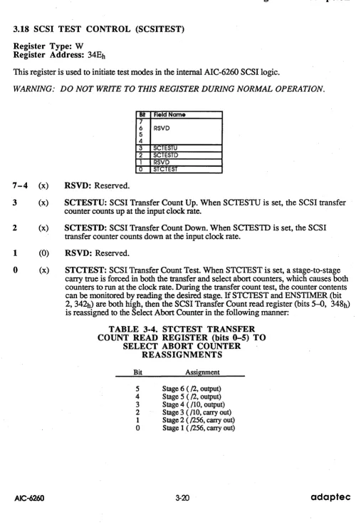
3.18 SCSI TEST CONTROL (SCSITEST) Register Type: W
Register Address: 34Eh
This register is used to initiate test modes in the internal AIC-6260 SCSI logic.
WARNING: DO NOT WRITE TO THIS REGISTER DURING NORMAL OPERATION.
Bit Field Name
7
6 RSVD 5
4
3 SCTESTU
2 SCTESTD
1 RSVD
a STCTEST
7 -4 (x) RSVD: Reserved.
3 (x) SCTESTU: SCSI Transfer Count Up. When SCTESTU is set, the SCSI transfer counter counts up at the input clock rate.
2 (x) SCTESTD: SCSI Transfer Count Down. When SCTESTD is set, the SCSI transfer counter counts down at the input clock rate.
1 (0) RSVD: Reserved.
o
(x) STCTEST: SCSI Transfer Count Test. When STCTEST is set, a stage-to-stage carry true is forced in both the transfer and select abort counters, which causes both counters to run at the clock rate. During the transfer count test, the counter contents can be monitored by reading the desired stage.If"
STCfEST and ENS TIMER .(bit 2, 342h) are both high, then the SCSI Transfer Count read register (bits 5-0, 348h) is reassigned to the Select Abort Counter in the following manner:AIC-6260
TABLE 3-4. STCTEST TRANSFER COUNT READ REGISTER (bits 0-5) TO
SELECT ABORT COUNTER REASSIGNMENTS
Bit Assignment
5 Stage 6 (/2, output) 4 Stage 5 (/2, output) 3 Stage 4 (/lO, output) 2 Stage 3 ( /l0, carry out) 1 Stage 2 ( /256, carry out)
°
Stage 1 (/256, carry out) [image:32.613.51.558.49.792.2]3.19 SCSI STATUS 4 (SSTAT4) Register Type: R
Register Address: 34Fh
This register contains status information on error conditions for the current SCSI transfer.
Bit Field Name
7 6
5 RSVD
4
3
2 SYNCERR 1 FWERR
0 FRERR
7-3
(0)
RSVD: Reserved. This field always reads as OOOOh.2 (0) SYNCERR: Synchronous Transfer Error. SYNCERR is set for one of the following two conditions:
1)
At the beginning of an inbound synchronous transfer, when the SCSI FIFO is not empty prior to the transfer of the first byte off the SCSI bus. This condition may cause the SCSI FIFO to overflow, as SCSICNT (bits 7-4, 34Eh, R) is not correct.2) At the beginning of a synchronous transfer, SOFFSET (bit 5, 34Dh) is set. This condition indicates that the previous transfer did not complete
successfully.
1 (0) FWERR: FIFO Write Error. FWERR is set when more than one source is enabled to write to the SCSI FIFO. This error can arise under the following condition:
The transfer path is set up to send data from the host FIFO, through the SCSI FIFO, onto the SCSI bus, with the AIC-6260 reselected as an Initiator and the target driving I/O such that data is enabled SCSI bus-to-SCSI FIFO (Data In
phase).
Section Three
Register Description
3.20 CLEAR SCSI ERRORS (CLRSERR)
Register Type: W
Register Address:
34FhThis register clears the error condition status bits in SSTAT4 (34Fh). Setting any of these bits clears the corresponding status bit. A clear bit does not need to be cleared before it can be set again. Writing a zero to any bit in this register has no effect. .
7-3 (0)
2 (0)
1
(0)
o
(0)
AIC-6260
Bit Field Name
7 6
5 RSVD
4 3
2 CLRSYNCERR
1 CLRFWERR 0 CLRFRERR
RSVD: Reserved.
CLRSYNCERR: Clear Synchronous Transfer Error. When CLRSYNCERR is set, the SYNCERR status bit is cleared (bit 2, 34Fh, R).
CLRFWERR: Clear FIFO Write Error. When CLRFWERR is set, the FWERR status bit is cleared (bit 1, 34Fh, R).
CLRFRERR: Clear FIFO Read Error. When CLRFRERR is set, the FRERR status bit is cleared (bit 0, 34Fh, R).
3.21 SCSI INTERRUPT MODE 0 (SIMODEO)
Register Type: R/W
Register Address: 350h
This register enables the interrupts associated with the status bits in SSTA TO (34Bh). Setting any of these bits enables the corresponding interrupt. If an event occurs that causes a status bit to be set, and the enable bit for that condition is set, IRQ is asserted.
Clearing an enable bit causes the interrupt associated with the condition to be masked. However, the status bit associated with the condition is still set, regardless of the state of the enable bits.
Bit Field Name 7 RSVD
6 ENSELDO
5 ENSELDI
4 ENSELINGO
3 ENSWRAP
2 ENSDONE
1 ENSPIORDY 0 ENDMADONE
7 (0) RSVD: Reserved. This bit always reads as O.
6 (x) ENSELDO: Enable Selection Done Out Interrupt. If ENSELDO is set, the SELDO interrupt is generated when SELDO (bit 6, 34Bh, R) is set.
S (x) ENSELDI: Enable Selection Done In Interrupt. IfENSELDI is set, the SELDI interrupt is generated when SELDI (bit 5, 34Bh, R) is set.
4 (x) ENSELINGO: Enable Selection Initiated Out Interrupt. If ENSELINGO is set, the SELINGO interrupt is generated when SELINGO (bit 4, 34Bh, R) is set.
3 (x) ENSWRAP: Enable Wrap Interrupt. If ENSWRAP is set, the SWRAP interrupt is generated when SWRAP (bit 3, 34Bh, R) is set.
2 (x) ENSDONE: Enable SCSI Done Interrupt. If ENS DONE is set, the SDONE interrupt is generated when SDONE (bit 2, 34Bh, R) is set.
1 (x) ENSPIORDY: Enable SCSI PIO.Ready Interrupt. IfENSPIORDY is set, the SPIORDY interrupt is generated when SPIORDY (bit 1, 34Bh, R) is set.
Section Three
Register Description
3.22 SCSI INTERRUPT MODE I (SIMODEI)
Register Type:
R/W
Register Address:
35lhThis register enables the interrupts associated with the status bits in SST A Tl (34Ch). Setting any of these bits enables the corresponding interrupt. If an event occurs causing a status bit to be set, and the enable bit for that condition is set, IRQ is asserted.
Clearing an enable bit causes the interrupt associated with the condition to be masked. However, the status bit associated with the condition is still set, regardless of the state of the enable bits.
Bit FieldName . 7 ENSELTIMO
6 ENATNTARG
5 ENSCSIRST
4 ENPHASEMIS
3 ENBUSFREE
2 ENSCSIPERR
1 ENPHASECHG
0 ENREQINIT
7
(x)
ENSELTIMO: Enable Selection Timeout Interrupt. If ENSELTIMO is set, the SELTO interrupt is generated when SELTO (bit 7, 34Ch, R) is set.6
(x)
ENATNT ARG: Enable Target Attention Interrupt. If ENA TNT ARG is set, the A TNT ARG interrupt is generated when A TNT ARG (bit 6, 34Ch, R) is set.S
(x)
ENSCSIRST: Enable SCSI Reset Interrupt. If ENSCSIRST is set, the SCSIRSTI interrupt is generated when SCSIRSTI (bit 5, 34Ch, R) is set.4
(x)
ENPHASEMIS: Enable Phase Mismatch Interrupt. If ENPHASEMIS is set, the PHASEMIS interrupt is generated when PHASEMIS (bit 4, 34Ch, R) is set.3
(x)
ENBUSFREE: Enable Bus Free Interrupt. If ENBUSFREE is set, the BUSFREE interrupt is generated when BUSFREE (bit 3, 34Ch, R) is set.2
(x)
ENSCSIPERR: Enable SCSI Parity Error Interrupt. If ENSCSIPERR is set, the SCSIPERR interrupt is generated when SCSIPERR (bit 2, 34Ch, R) is set.I
(x)
ENPHASECHG: Enable Phase Change Interrupt. If ENPHASECHG is set, the PHASECHG interrupt is generated when PHASECHG (bit l, 34Ch, R) is set.0
(x)
ENREQINIT: Enable REQ Initiated Interrupt. When ENREQINIT is set, the REQINIT interrupt is generated when REQINIT (bit 0, 34Ch, R) is set.3.23 DMA CONTROL 0 (DMACNTRLO)
Register Type:
RIW
Register Address:
352hThis register contains the basic controls for PIO and DMA transfer modes. The bits which enable a mode may be set at the same time as the bits configuring the mode.
Bit Field Name 7 ENDMA
6 8BIT /- 16BIT
5 DMA/-PIO
4 RSVD
3 WRITE/-READ
2 INTEN
1 RSTFIFO
0 SWINT
7
(0)
ENDMA: Enable DMA. When ENDMA is set, data transfer between host main memory and the host FIFO in either PIO or DMA mode is enabled.Clearing ENDMA also clears A TDONE (bit 7, 354h).
6 (x) 8BIT/-16BIT: 8-Bit/-16-Bit Mode. When this bit is set, transfers between host main memory and the host FIFO are 8 bits wide and utilize SDO-SD7. When this bit is cleared, transfers between host main memory and the host FIFO are 16 bits wide and utilize SDO-SDI5. Transfers utilizing host DMA mode are 8 bits wide.
5 (x) DMAI-PIO: DMA/-PIO Mode. When this bit is set, transfers between host main memory and the host FIFO are in DMA mode. When this bit is cleared, transfers between host main memory and the host FIFO are in PIO mode.
NOTE: When changing from PIa toDMA withENDMA
=
1, any direction change must be done first (bit 3 below.)4 (0) RSVD: Reserved. This bit always reads O.
3
(x)
WRITE/-READ: Transfer Direction. When this bit is set, data is transferred from host main memory to the host FIFO. When this bit is cleared, data is transferred from the host FIFO to host main memory.2
(x)
INTEN: Master Interrupt Enable. INTEN controls the assertion of the IRQ pin. If INTEN is set, interrupts function normally. IfINTEN is cleared, all interrupts are masked.1
(x)
RSTFIFO: Reset FIFO Counter. When RSTFIFO is set, the FIFO counter (bits 7-0, 355h) is cleared. RSTFIFO is a self-clearing bit.Section Three
Register Description
3.24 DMA CONTROL 1 (DMACNTRLl) Register Type:
RIW
Register Address: 353h
This register is used to set the power-down feature and write the stack offset pointer.
7
(0)
6-4 (0) 3-0 (x)
AIC-6260
Bit Field Name
7 PWRDWN
6
5 RSVD 4
3 2 STK
1 0
PWRDWN: Power Down. When PWRDWN is set, the internal clock is stopped to conserve power. Once the clock is stopped, the AIC-6260 is not operational.
RSVD: Reserved.
STK: Stack Offset Pointer. STK contains the stack offset pointer. This field is write-only.
3.25 DMA STATUS (DMAST AT) Register Type: R
Register Address: 354h
This register reflects the real-time status of the current DMA or PIO transfer.
Bit Field Name
7 ATDONE
6 WORDRDY
5 INTSTAT
4 DFIFOFULL
3 DFIFOEMP
2
1 RSVD
0
7
(x)
ATDONE: host Done. ATDONE is used in DMA mode only. This bit is set whenthe host DMA controller has transferred the last byte or word and asserted TIC.
While A TOONE is set, the internal host DMA logic is disabled; the host DMA logic remains disabled until this bit is cleared. A TDONE is cleared when ENDMA (bit 7,
352h) is cleared.
A TDONE does not generate an interrupt.
6
(x)
WORDRDY: Word Ready. WORDRDY is used in PIO mode only. WhenWORDRDY is set, a 16-bit word is ready for transfer to or from the host FIFO. If
the transfer count for a particular transfer does not equal or end on a 128-byte boundary, the host must transfer data into or out of the host FIFO one word at a time; this bit is used to control that process.
5
(x)
INTST AT: Interrupt Status. INTST A T is the OR of all enabled interrupts.INTSTA T may be read. at any time, whether or not interrupts have been enabled via
INTEN. This provides a means to poll for interrupts.
4
(x)
DFIFOFULL: host FIFO Full. DFIFOFULL is set when the host FIFO is full. DFIFOFULL is used during SCSI-to-host PIa transfers.3 (x) DFIFOEMP: host FIFO Empty. DFIFOEMP is set when the host FIFO is empty. DFIFOEMP is used during host-to-SCSI PIO transfers.
Section Three
3.26 FIFO STATUS (FIFOST A T) Register Type: R
Register Address: 355h
Register Description
This register provides a count of the current number of bytes in the host FIFO.
7-0 (x)
AIC-6260
Bit Field Name
7 FCNT (MSB)
0 FCNT (lSB)
FCNT: FIFO Count. FCNT contains a count of the of bytes in the host FIFO.
NOTE: The host FIFO is 128 bytes deep. Under some circumstances, the host FIFO may hold up to 4 additional bytes (132 bytes
J.
FCNT contains the co"ect count in these circumstances.3.27 DATA -PORT (DATAPORTL and DATAPORTH) Register Type: R/W
Register Address: 356h
Data transfers between the AIC-6260 and the host take place via this register in both DMA and PIO mode. DMA transfers are 8-bit only. host PIO transfers are 8- or 16-bit, as defined by the state of SBHE. If SBHE is not active, 8 bits will be transferred via the low order data byte; if SBHE is active, 16 bits will be transferred.
15-8 (x)
7-0 (x)
Field Name
DATAH (MSB)
DATAH (LSB) DATAL (MSB)
o
DATAL (LSB)DATAH: High-Order Data Byte. This byte is valid only if 8BIT/-16BIT (bit 6, 352h) is cleared or SBHE is asserted.
Section Three
3.28 BURST CONTROL (BRSTCNTRL) Register Type: R/W
Register Address: 358h
Register Description
This register controls the burst on and burst off times for DMA transfers. The AIC-6260 will run as many Burst On/Burst Off cycles as necessary to transfer all data. To disable the BON and BOFF timers, load both BON and BOFF withOOOOh.
Bit Field Name
7 6 BON 5 4
3
2 BOFF
1 0
7-4 (x) BON: Burst On. BON contains the maximum value, in microseconds, of the transmission (burst) period. The AIC-6260 bursts data for the duration of BON, or until all data has been sent, whichever is less. BON may range from 0 (none) to 15 microseconds.
3-0 (x) BOFF: Burst Off. BOFF contains the minimum value, in microseconds, of the off-line (down) period. The AIC-6260 will not request DMA serviCe for at least the duration of BOFF. BOFF may range from 0 (none) to 15 microseconds.
3.29 PORT A (PORT A) Register Type:
RIW
Register Address: 35Ah
This register provides an external 8- or 16-bit port which may be accessed at any time. Port A is user-defined.
3.30 PORT B (PORTB) Register Type: R/W Register Address: 35Bh
This register provides an external 8- or 16-bit port which may be accessed at any time. Port B is user-defined.
3.31 REVISION (REV) Register Type: R
Register Address: 35Ch
This register gives the revision level of the chip in bits 2--0. Revision level 1 returns a value of Oh.
3.32 STACK (STACK) Register Type: R/W Register Address: 35Dh
This register is a 16-byte stack for general purpose memory use. The stack port may be addressed by writing to the lower 4 bits of DMACNTRL1 (353h). The offset points to the fIrst location in the stack to be read from or written to. This allows the software to directly access any byte in the stack. Successive reads or writes access the next higher location in the stack.
3.33 TEST REGISTER (TEST) Register Type: W
Register Address: 35Eh
This register is used for test purposes only, and should not be written to during normal operation. During testing, either SCSmLK or DMABLK should be set, but not both bits. To operate a specifIc test, one bit of bits 6-2 may be set.
Bit Field Name
7 RSVD
6 BOFFTMR
"s BONTMR
4 STCNTH 3 STCNTM
2 STCNTL
1 SCSIBLK
0 DMABLK
7 (0) RSVD: Reserved.
6
(x)
BOFFTMR: Buffer Off Timer. When BOFFfMR is set with either SCSIBLK or DMABLK set, the BOFFfMR [7:0] to SCD [7:0] test path is enabled.5
(x)
BONTMR: Buffer On Timer. When BONTMR is set with either SCSIBLK or DMABLK set, the BONTMR [7:0] to SCD [7:0] test path is enabled.4
(x)
STCNTH: SCSI Transfer High Count. When STCNTH is set with either SCSIBLK or DMABLK set, the SCSI transfer counter [23: 16] to SD [15:8] test path is enabled.3
(x)
STCNTM: SCSI Transfer Mid Count. When STCNTM is set with eitherSCSIBLK or DMABLK set, the SCSI transfer counter [15:8] to SD [15:8] test path is enabled.
2
(x)
STCNTL: SCSI Transfer Low Count. When STCNTL set with either SCSmLK or DMABLK set, the SCSI transfer counter [7:0] to SD [15:8] test path is enabled.1 (x) SCSIBLK: SCSI Block. When SCSIBLK is set, the internal AIC-6260 SCSI logic is configured for testing. Pin redefInitions are given in Table 3-5.
Section Three
Register Description
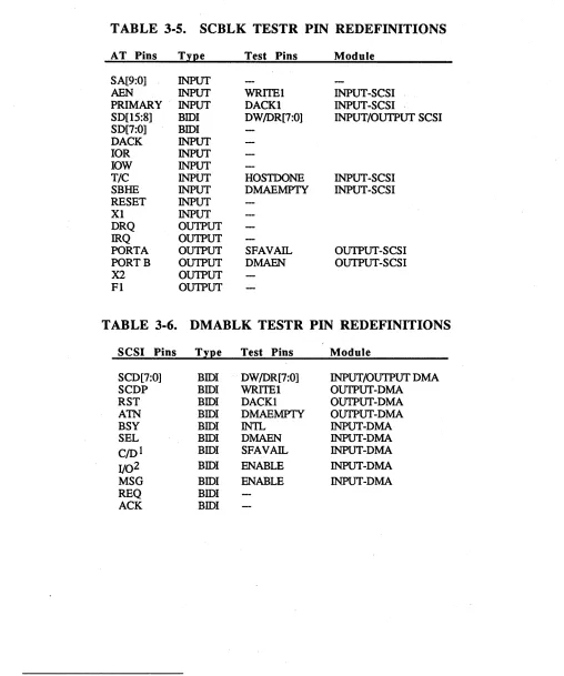
TABLE 3·5. SCBLK TESTR PIN REDEFINITIONS
AT Pins TIl!e Test Pins Module
SA[9:0] INPUT
AEN INPUT WRITE I INPUT-SCSI PRIMARY INPUT DACKl INPUT-SCSI
SD[15:8] BIDI DWIDR[7:0] INPUT/OUTPUT SCSI SD[7:0] BIDI
DACK INPUT lOR INPUT lOW INPUT
T/C INPUT HOSTDONE INPUT-SCSI SBHE INPUT DMAEMPTY INPUT-SCSI RESET INPUT
Xl INPUT DRQ OUTPUT IRQ OUTPUT
PORTA OUTPUT SFAVAIL OUTPUT-SCSI PORTB OUTPUT DMAEN OUTPUT-SCSI
X2 OUTPUT FI OUTPUT
TABLE 3·6. DMABLK TESTR PIN REDEFINITIONS
SCSI Pins TIl!e Test Pins Module
SCD[7:0] BIDI DWIDR[7:0] INPUT/OUTPUT DMA SCDP BIDI WRlTEl OUTPUT-DMA RST BIDI DACKI OUTPUT-DMA AlN BIDI DMAEMPTY OUTPUT-DMA BSY BIDI INTL INPUT-DMA SEL BIDI DMAEN INPUT-DMA C/O! BIDI SFAVAIL INPUT-DMA
1/02 BIDI ENABLE INPUT-DMA
MSG BIDI ENABLE INPUT-DMA REQ BIDI
ACK BIDI
1 I/O: In addition to setting bit 0, I/O must be set to enable DWl[7:0] on SCD [7:0]. The enable is only used when transferring data from the host to SCSI.
2 MSG: MSG is used to enable WRITEl, DACKl, and DMAEMPTY.
[image:44.612.53.561.60.669.2]The AIC-6260 is a single-chip SCSI Host Adapter with which the features and advantages of SCSI can be realized on the motherboard in PC A T systems. The AIC-6260 is an appropriate choice in systems ranging from laptops and notebooks all the way up to workstations.
The AIC-6260 has everything necessary to implement a SCSI interface in a single package. Through its register based host interface, it can be configured to operate as either a SCSI initiator or target with asynchronous or synchronous SCSI data transfers. To offload the host processor, SCSI data transfers may be perfonned with little or no host intervention using "SCSI Nonnal" transfer mode. Altem(l,tively the host may have complete control over SCSI data transfers by selecting "SCSI Manual PIO" or "SCSI AutomaticPIO" transfer mode.
Data transfers over the host bus may be accomplished using either "Host PIO" or "Second Party DMA" transfers. The AIC-6260 can be configured to generate interrupts for all timing critical SCSI operations. The AIC-6260 also provides a decoded address output simplifying the setup of 2 general purpose I/O ports( A and B). To aid in programming, the chip features a 16-byte stack accessible and controllable by the host processor.
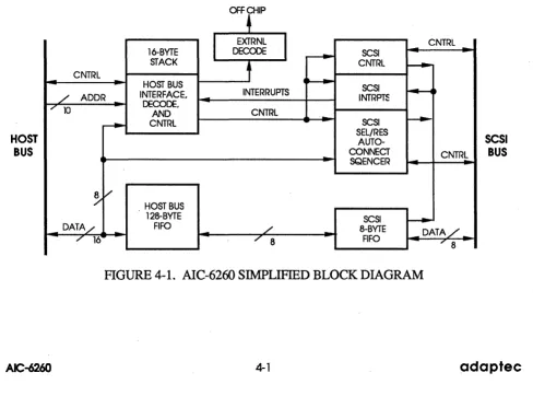
4.1 GENERAL FUNCTIONAL DESCRIPTION
This section describes the general operation and major components of the AIC-6260. Figure 4-1 is a simplified block diagram of the device. '
HOST BUS
CNTRL
/ ' ADDR / 10
~
~
/'_ DATAL ,/ 16
16-BYTE STACK HOST BUS INTERFACE, DECODE, AND CNTRL HOST BUS 128-BYTE FIFO OFF CHIP
~
I
EXTRNLI
DECOOE
~
,
..
INTERRUPTS
CNTRL
'.
...
-
L...
,/ 8
SCSI CNTRL SCSI INTRPTS SCSI SEL/RES AUTO-CONNECT SQENCER SCSI 8-BYTE FIFO CNTRL