Application Note No. 143
A Low-Cost Low Noise Amplifier + Bandpass Filter
Rx Front End for Improved-Sensi
ti
vity / Enhanced
Range 315 and 434 MHz RKE Applications using
the ESD-Robust BFP460 RF Transistor
All Rights Reserved. LEGAL DISCLAIMER
THE INFORMATION GIVEN IN THIS APPLICATION NOTE IS GIVEN AS A HINT FOR THE IMPLEMENTATION OF THE INFINEON TECHNOLOGIES COMPONENT ONLY AND SHALL NOT BE REGARDED AS ANY DESCRIPTION OR WARRANTY OF A CERTAIN FUNCTIONALITY, CONDITION OR QUALITY OF THE INFINEON TECHNOLOGIES COMPONENT. THE RECIPIENT OF THIS APPLICATION NOTE MUST VERIFY ANY FUNCTION DESCRIBED HEREIN IN THE REAL APPLICATION. INFINEON TECHNOLOGIES HEREBY DISCLAIMS ANY AND ALL WARRANTIES AND LIABILITIES OF ANY KIND (INCLUDING WITHOUT
LIMITATION WARRANTIES OF NON-INFRINGEMENT OF INTELLECTUAL PROPERTY RIGHTS OF ANY THIRD PARTY) WITH RESPECT TO ANY AND ALL INFORMATION GIVEN IN THIS APPLICATION NOTE.
Information
For further information on technology, delivery terms and conditions and prices please contact your nearest Infineon Technologies Office (www.infineon.com).
Warnings
Due to technical requirements components may contain dangerous substances. For information on the types in question please contact your nearest Infineon Technologies Office.
Infineon Technologies Components may only be used in life-support devices or systems with the express written approval of Infineon Technologies, if a failure of such components can reasonably be expected to cause the failure of that life-support device or system, or to affect the safety or effectiveness of that device or system. Life support devices or systems are intended to be implanted in the human body, or to support and/or maintain and sustain and/or protect human life. If they fail, it is reasonable to assume that the health of the user or other persons may be endangered.
Application Note 3 Rev. 1.2, 2008-02-19
Application Note No. 143
Revision History: 2008-02-19, Rev. 1.2 Previous Version: 2004-08-02, Rev. 1.1
Page Subjects (major changes since last revision)
Application Note 4 Rev. 1.2, 2008-02-19
1
A Low-Cost Low Noise Amplifier + Bandpass Filter Rx Front End
for Improved-Sensivity / Enhanced Range 315 and 434 MHz RKE
Applications using the ESD-Robust BFP460 RF Transistor
Overview
• The Infineon BFP460 "EHRT" (ESD-Hardened RF Transistor) is investigated for use as a low-current, wideband feedback LNA to demonstrate feasibility as an external LNA for boosting sensitivity / range of Infineon Technologies' Remote Keyless Entry (RKE) ICs in the TDA52x0 / TDA52x1 family
• The BFP460 is specially designed for improved robustness against Electro Static Discharge (ESD) events and is rated for 1500 V ESD between any pair of terminals, using the Human Body Model (HBM).
• The test board includes an optional, simple, low-cost, lumped element bandpass filter tuned for 315 MHz which follows the BFP460 LNA stage. The filter may be re-tuned for 434 MHz. The addendum in Appendix A shows the 434 MHz filter, and LNA + Filter performance. The applications PC board is set up such that either the LNA or the Bandpass filter may be tested alone, or the cascade of LNA + Bandpass filter may be tested as a complete chain.
Figure 1 Block Diagram
Design Goals
• LNA: Gain > 15 dB, Noise Figure < 2.0 dB, Input / Output Return Loss 10 dB or better over the entire 300 - 928 MHz frequency range, current < 5 mA. Provide one external LNA solution that is usable over the 315 - 900 MHz frequency range, for improving sensitivity / range of the Infineon Technologies Remote Keyless Entry (RKE) receiver products TDA52x0 / TDA52x1 in a variety of applications. Note this LNA should improve range of TDA52xx by a factor of approximately two. It has been verified in the lab that there is 5 - 6 dB improvement in sensitivity with a similar external LNA and TDA5211 receiver IC.
• Bandpass Filter: provide for rejection / attenuation of potential "receiver blocking" signals arising from FM or TV broadcast emitters, cellular phones or base stations, etc. Do this with minimal use of components, at minimal cost. Note filter uses only 2 chip inductors and 5 chip capacitors. Filter shown in this document is set up for
f
0= 315 MHz, but it may be re-tuned for 434 MHz.$1BEORFNBGLDJUDPYVG %DQGSDVV)LOWHU I 0+] 7RS&&RXSOHG&KHE\VKHY LQGXFWRUVFDSDFLWRUV ,QVHUWLRQ/RVV#0+] G% )LOWHUPD\EHUHWXQHGIRU0+] %)3/1$ *DLQ G%#0+] 1) G%#0+] 9&& 9,& P$ - - 7RWHVW/1$DORQH,QSXWDW-RXWSXWDW- 7RWHVWEDQGSDVVILOWHUDORQH,QDW-RXWDW-
7RWHVWFDVFDGHRI/1$)LOWHU,QDW-RXWDW-Application Note 5 Rev. 1.2, 2008-02-19 Potential target markets for TDA52xx RKE products requiring improved sensitivity / improved range (e.g. requiring external LNAs) include:
• NAFTA automotive market for remote keyless entry systems (RKE) at 315 MHz
• Security market at 345 MHz, 433.92 MHz (e.g. alarm systems controlled with radio links) • Garage door opener market, 390 MHz range
• European automotive RKE market at 434 MHz
• Various 900 MHz ISM Band Applications in the 902-928 NAFTA ISM Band
Printed Circuit Board is P/N 460-021104 Rev B. Standard FR4 material is used in a simple 3 layer design. Low-cost, standard SMT passive components of "0402" case size are used throughout. No chip coils are required for this LNA design, further reducing cost. (Only resistors and capacitors are required for the LNA). The optional bandpass filter uses 2 chip coils and 5 chip capacitors. Refer to cross sectional diagram schematic diagram and Bill Of Material (BOM).
PC Board Cross-Sectional Diagram
Figure 2 PCB - Cross Sectional Diagram
The LNA is unconditionally stable from 5 MHz to 6 GHz.
Total PCB area used for the single LNA stage is approximately 50 mm². Total Parts count, including the BFP460 transistor, is 10. Total area for 315 MHz bandpass filter is approx. 40mm².
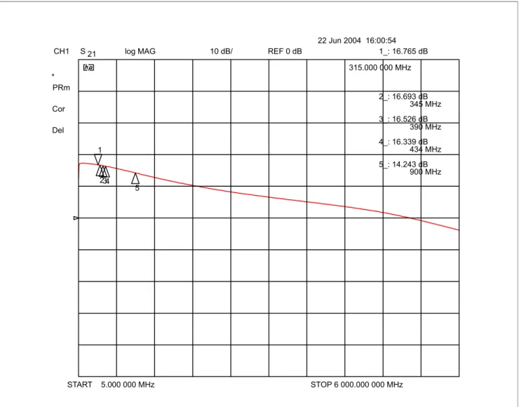
LNA: Achieved ≅16.8 dB gain, 1.5 dB Noise Figure @ 315 MHz, from a 5.0 V supply drawing 5.2 mA. Note usable gain, good input / output matching and < 2 dB noise figure is achieved over the entire 300 - 1000 MHz range in this wideband design. Note noise figure result does NOT "back out" FR4 PCB losses - if the PCB loss at LNA input were extracted, Noise Figure result would be approximately 0.1 to 0.2 dB lower.
$1B3&%YVG %27720/$<(5 LQFKPP LQFKPP" 723/$<(5 ,17(51$/*5281'3/$1( /$<(5)250(&+$1,&$/5,*,',7<2)3&%7+,&.1(66+(5(127 &5,7,&$/$6/21*$6727$/3&%7+,&.1(66'2(6127(;&((' ,1&+PP63(&,),&$7,21)25727$/3&%7+,&.1(66 ,1&+PPPP 7+,663$&,1*&5,7,&$/
Application Note 6 Rev. 1.2, 2008-02-19
Summary of LNA Data
T
= 25 °C, network analyzer source power = -25 dBmTable 1 Summary of LNA Data
Parameter Result Comments
Frequency Range 300 - 1000 MHz 315, 345, 390, 434 & 900 MHz ISM bands covered
DC Current 5.2 mA
DC Voltage,
V
CC 5.0 V 5.0 V standard in automotiveapplications
Collector-Emitter Voltage,
V
CE 3.1 V BFP460V
CE MAX= 4.5 VGain 16.8 dB @ 315 MHz 16.3 dB @ 434 MHz 14.2 dB 9 0 MHz Noise Figure 1.5 dB @ 315 MHz 1.5 dB @ 434 MHz 1.4 dB @ 900 MHz
These values do not extract PCB losses, etc. resulting from FR4 board an passives used on PCB - these results are at input SMA connector.
See Figure 4 and Table 5. Input Return Loss 13.5 dB @ 315 MHz
13.0 dB @ 434 MHz 11.2 dB @ 900 MHz
Good broadband match.
Output Return Loss 21.2 dB @ 315 MHz 19.6 dB @ 434 MHz 15.3 dB @ 900 MHz
Good broadband match.
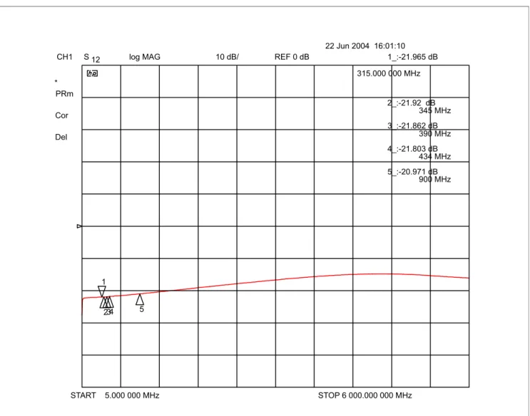
Reverse Isolation 21.9 dB @ 315 MHz 21.8 dB @ 434 MHz 21.0 dB @ 900 MHz
Application Note 7 Rev. 1.2, 2008-02-19
Summary of 315 MHz Bandpass Filter Data
T
= 25 °C, network analyzer source power = -25 dBmPlease refer to network analyzer plots of Bandpass Filter which appear later in this document.
Table 2 Summary of 315 MHz Bandpass Filter Data
Parameter Result Comments
Center Frequency 315 MHz Top-C Coupled Bandpass Filter, with 2 coils and 5 capacitors. May be re-tuned for 434 MHz applications. Insertion Loss 2.4 dB @ 315 MHz Insertion loss may be further
optimized by using higher-Q chip coils. Coils used are low-cost versions and have Q values of approx. 35 at 300 MHz. Attenuation at 216 MHz, relative to
insertion loss at 315 MHz
30.1 dB Upper edge of Television Channel 13 in North America (potential "blocker" for 315 MHz receiver). See
Figure 25 and Figure 26. Input Return Loss 13.0 dB @ 315 MHz
Output Return Loss 13.7 dB @ 315 MHz Asymmetry between S11 and S22 due to PC board - refer to PCB scanned images.
Application Note 8 Rev. 1.2, 2008-02-19
Summary of Cascade (LNA + Bandpass Filter together) Data
T
= 25 °C, network analyzer source power = -25 dBmPlease refer to network analyzer screen-shots at end of this document to get a better idea of performance of LNA + Filter Cascade.
Table 3 Summary of Cascade Data, 315 MHz
Parameter Result Comments
Frequency Range 315 MHz Bandpass filter following LNA causes limitation of bandwidth. Filter may be re-tuned for other
frequencies of interest. DC Current 5.2 mA
DC Voltage,
V
CC 5.0 V 5.0 V standard in automotiveapplications
Collector-Emitter Voltage,
V
CE 3.1 V BFP460V
CE MAX = 4.5 V Gain 14.4 d 315 MHzNoise Figure 1.6 dB @ 315 MHz These values do not extract PCB losses, etc. resulting from FR4 board an passives used on PCB - these results are at input SMA connector.
See pages Figure 5 and Table 6. Input
P
1dB -20.1 dB @ 315 MHz See input power sweep vs. gain plot,Figure 9.
Input 3rd Order Intercept -10.6 dBm @ 315 MHz Two tones, 314.5 MHz and
315.5 MHz, -33 dBm per tone. Input Return Loss 18.0 dB @ 315 MHz
Output Return Loss 12.7 dB @ 315 MHz Reverse Isolation 24.4 dB @ 315 MHz
Application Note 9 Rev. 1.2, 2008-02-19
Bill of Material
Broadband BFP460 UHF Feedback LNA (Yellow shading) and Lumped-Element Top-C Coupled Bandpass Filter (Blue Shading)
Table 4 Bill of Material for 315 MHz variant Reference
Designator
Value Manufacturer Case Size Function
C1 390 pF Various 0402 DC blocking, input.
C2 390 pF Various 0402 DC block for feedback network. C3 390 pF or
10 pF
Various 0402 For LNA alone, output DC block 390 pF. If bandpass filter is used, then C3 = 10 pF, serves as DC block & filter element. C4 0.1µF Various 0402 Decoupling, low frequency.
C5 390 pF Various 0402 Decoupling.
R1 110 kΩ Various 0402 DC bias for base of Q1. R2 560Ω Various 0402 Feedback resistor for LNA
R3 300Ω Various 0402 Bring DC to collector, high resistor values does not load LNA output.
R4 130Ω Various 0402 Provides some negative feedback for DC bias / DC operating point to compensate for variations in transistor DC current gain, temperature variations, etc. Also drops 5 V down to 4.4 V (below maximum collector-emitter voltage for BFP540F).
Q1 - Infineon Technologies SOT343 BFP460EHRT ESD-Robust Transistor (1500 V HBM).
f
T= 22 GHzJ1, J2, J3 - Johnson 142-0701-841 - RF input / output connectors J4 - AMP 5 pin header
MTA-100 series 640456-5 (standard pin plating) or 641215-5 (gold plated pins) - DC connector Pins 1, 5 = ground Pin 3 =
V
CC Pins 2, 4 = no connection L1, L2 5.6 nH Coilcraft 0402CS-5N6XJBU chip inductor0402 Coil for shunt resonators in bandpass filter.
C6, C8 30 pF Various 0402 Capacitor for shunt resonators in bandpass filter.
C7 5.6 pF Various 0402 Coupling cap between filter resonators. C9 10 pF Various 0402 Output cap of filter.
Application Note 10 Rev. 1.2, 2008-02-19
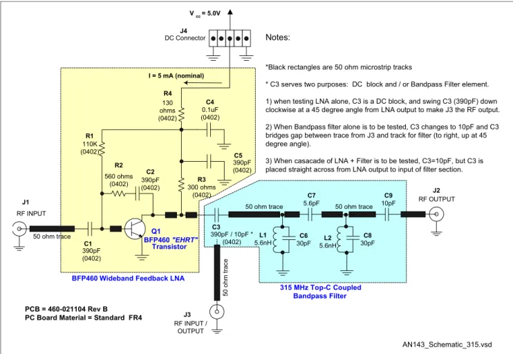
Schematic Diagram for UHF LNA and Optional 315 MHz Bandpass Filter
Note low parts count and simple design. No chip inductors are required for the LNA.
Figure 3 Schematic Diagram for UHF LNA and Optional 315 MHz Bandpass Filter
$1B6FKHPDWLFBYVG 3&% 5HY% 3&%RDUG0DWHULDO 6WDQGDUG)5 4 %)3(+57 7UDQVLVWRU -5),1387 & S) , P$QRPLQDO 5 . & S) 5 RKPV & X) 9FF 9 -'&&RQQHFWRU -5)287387 & S)S) 5 RKPV & S) 5 RKPV -5),1387 287387 & S) & S) 1RWHV %ODFNUHFWDQJOHVDUHRKPPLFURVWULSWUDFNV &VHUYHVWZRSXUSRVHV'&EORFNDQGRU%DQGSDVV)LOWHUHOHPHQW ZKHQWHVWLQJ/1$DORQH&LVD'&EORFNDQGVZLQJ&S)GRZQ FORFNZLVHDWDGHJUHHDQJOHIURP/1$RXWSXWWRPDNH-WKH5)RXWSXW :KHQ%DQGSDVVILOWHUDORQHLVWREHWHVWHG&FKDQJHVWRS)DQG& EULGJHVJDSEHWZHHQWUDFHIURP-DQGWUDFNIRUILOWHUWRULJKWXSDW GHJUHHDQJOH :KHQFDVDFDGHRI/1$)LOWHULVWREHWHVWHG& S)EXW&LV SODFHGVWUDLJKWDFURVVIURP/1$RXWSXWWRLQSXWRIILOWHUVHFWLRQ / Q+ & S) / Q+ 0+]7RS&&RXSOHG %DQGSDVV)LOWHU %)3:LGHEDQG)HHGEDFN/1$ RKPWUDFH RKPWUDFH RKPWUDFH RKP WU D F H & S)
Application Note 11 Rev. 1.2, 2008-02-19
Noise Figure, Plot, LNA alone, Center of Plot (x-axis) is 1065 MHz.
Figure 4 Noise Figure of LNA alone @ 315 MHz
$1BSORWBQIB/1$BYVG 5RKGH 6FKZDU])6(. 1RLVH)LJXUH /1$$ORQH -XQ (871DPH %)3%URDGEDQG8+))HHGEDFN/1$ 0DQXIDFWXUHU ,QILQHRQ7HFKQRORJLHV 2SHUDWLQJ&RQGLWLRQV 9 9, P$7 & 2SHUDWRU1DPH *HUDUG:HYHUV 7HVW6SHFLILFDWLRQ /:56'/1$35HYLVLRQ' &RPPHQW 3&%5HY% -XQH $QDO\]HU 5)$WW G% 5HI/YO G%P 5%: 0+] 9%: +] 5DQJH G% 5HI/YODXWR 21 0HDVXUHPHQW QGVWDJHFRUU 21 0RGH 'LUHFW (15 +3$(15 0+] 0+]',9 0+] 1RLVH)LJXUHG%
Application Note 12 Rev. 1.2, 2008-02-19
Noise Figure, LNA alone, Tabular Data
From Rohde & Schwarz FSEK3 + FSEM30 System Preamplifier = MITEQ SMC-02
Table 5 Noise Figure LNA @ 315 MHz
Frequency Noise Figure
115 MHz 1.42 dB 215 MHz 1.40 dB 315 MHz 1.50 dB 415 MHz 1.52 dB 515 MHz 1.52 dB 615 MHz 1.52 dB 715 MHz 1.47 dB 815 MHz 1.41 dB 915 MHz 1.42 dB 1015 MHz 1.41 dB 1115 MHz 1.48 dB 1215 MHz 1.50 dB 1315 MHz 1.54 dB 1415 MHz 1.57 dB 1515 MHz 1.62 dB 1615 MHz 1.67 dB 1715 MHz 1.70 dB 1815 MHz 1.82 dB 1915 MHz 1.89 dB 2015 MHz 1.92 dB
Application Note 13 Rev. 1.2, 2008-02-19
Noise Figure, Plot, Cascade of LNA + BPF, Center of Plot (x-axis) is 315 MHz.
Figure 5 Noise Figure of Cascade @ 434 MHz
$1BSORWBQIB&DVFDGHBYVG 5RKGH 6FKZDU])6(. 1RLVH)LJXUH /1$0+]%DQGSDVV)LOWHU -XQ (871DPH %)3%URDGEDQG8+))HHGEDFN/1$SOXV0+]/&%DQGSDVV)LOWHU 0DQXIDFWXUHU ,QILQHRQ7HFKQRORJLHV 2SHUDWLQJ&RQGLWLRQV 9 9, P$7 & 2SHUDWRU1DPH *HUDUG:HYHUV 7HVW6SHFLILFDWLRQ /:56'/1$35HYLVLRQ' &RPPHQW 3&%5HY% -XQH $QDO\]HU 5)$WW G% 5HI/YO G%P 5%: 0+] 9%: +] 5DQJH G% 5HI/YODXWR 21 0HDVXUHPHQW QGVWDJHFRUU 21 0RGH 'LUHFW (15 +3$(15 0+] 0+]',9 0+] 1RLVH)LJXUHG%
Application Note 14 Rev. 1.2, 2008-02-19
Noise Figure, Cascade of LNA + Bandpass Filter, Tabular Data
From Rohde & Schwarz FSEK3 + FSEM30
Table 6 Noise Figure Cascade @ 434 MHz
Frequency Noise Figure
250 MHz 3.08 dB 255 MHz 2.63 dB 260 MHz 2.33 dB 265 MHz 2.06 dB 270 MHz 1.90 dB 275 MHz 1.83 dB 280 MHz 1.72 dB 285 MHz 1.66 dB 290 MHz 1.61 dB 295 MHz 1.57 dB 300 MHz 1.57 dB 305 MHz 1.55 dB 310 MHz 1.57 dB 315 MHz 1.56 dB 320 MHz 1.57 dB 325 MHz 1.56 dB 330 MHz 1.57 dB 335 MHz 1.58 dB 340 MHz 1.60 dB 345 MHz 1.58 dB 350 MHz 1.63 dB 355 MHz 1.65 dB 360 MHz 1.70 dB 365 MHz 1.73 dB 370 MHz 1.77 dB 375 MHz 1.78 dB 380 MHz 1.86 dB
Application Note 15 Rev. 1.2, 2008-02-19
Scanned Image of PC Board
Application Note 16 Rev. 1.2, 2008-02-19
Scanned Image of PC Board, Close-In Shot, showing LNA and Optional Bandpass Filter
Figure 7 Image of PC Board, Close-In Shot
Application Note 17 Rev. 1.2, 2008-02-19
Stability Factor K and Stability Measure B1
Note that K > 1 and B1> 0, the amplifier is unconditionally stable. Measured LNA s-parameters were taken on a
Network Analyzer & then imported into GENESYS simulation package, which calculates and plots K and B1.
Figure 8 Plot of K(f) and B1(f)
Application Note 18 Rev. 1.2, 2008-02-19
Power Sweep at 315 MHz (CW), Cascade = LNA + Bandpass Filter
Source Power (Input) swept from -35 to -7 dBm Input
P
1dB≅-20.0 dBmFigure 9 Plot of Power Sweep @ 315 MHz
&+ 6 ORJ0$* G% 5()G% 67$57G%P &:0+] 6723G%P &RU 6PR 'HO 35P
0$5.(5
G%P
-XQ BG% G%P BG% G%P $1BSORWBSRZHUBVZHHSBYVGApplication Note 19 Rev. 1.2, 2008-02-19
Input 3rd Order Intercept Test, for Cascade of LNA + Bandpass Filter
Two Tones,
f
1= 314.5 MHz,f
2= 315.5 MHz, -33 dBm power each tone.Input
IP
3= -33 + (44.7 / 2) = -10.6 dBmFigure 10 Tow-Tone Test @ 315 MHz, LNA alone
Application Note 20 Rev. 1.2, 2008-02-19
Input Return Loss, Log Mag, Narrow Span, LNA alone
65 MHz - 565 MHz
Figure 11 Plot of Input Return Loss, Narrow Span, 315 MHz, LNA alone
&+ 6 ORJ0$* G% 5()G% &(17(50+] 63$10+] &RU 35P -XQ BG% 0+] BG% 0+] $1BSORWBLQSXWBUHWXUQBORVVBQDUURZB/1$BYVG
Application Note 21 Rev. 1.2, 2008-02-19
Input Return Loss, Smith Chart, Narrow Span, LNA alone
Reference Plane = PCB Input SMA Connector 65 MHz - 565 MHz
Figure 12 Smith Chart of Input Return Loss, Narrow Span, 315 MHz, LNA alone &+ 6 8)6 &(17(50+] 63$10+] &RU 35P -XQ B S) 0+] B 0+] $1BVPLWKBLQSXWBUHWXUQBORVVBQDUURZB/1$BYVG
Application Note 22 Rev. 1.2, 2008-02-19
Forward Gain, Narrow Span, LNA alone
65 MHz - 565 MHz
Figure 13 Plot of Forward Gain, Narrow Span, 315 MHz, LNA alone
&+ 6 ORJ0$* G% 5()G% &(17(50+] 63$10+] &RU 35P -XQ BG% 0+] BG% 0+] $1BSORWBIZBJDLQBQDUURZB/1$BYVG
Application Note 23 Rev. 1.2, 2008-02-19
Reverse Isolation, Narrow Span, LNA alone
65 MHz - 565 MHz
Figure 14 Plot of Reverse Isolation, Narrow Span, 315 MHz, LNA alone &+ 6 ORJ0$* G% 5()G% &(17(50+] 63$10+] &RU 35P -XQ BG% 0+] BG% 0+] $1BSORWBUHYHUVHBLVRODWLRQBQDUURZB/1$BYVG
Application Note 24 Rev. 1.2, 2008-02-19
Output Return Loss, Log Mag, Narrow Span, LNA alone
65 MHz - 565 MHz
Note good output return loss - makes integration with bandpass filter easier
Figure 15 Plot of Output Return Loss, Narrow Span, 315 MHz, LAN alone &+ 6 ORJ0$* G% 5()G% &(17(50+] 63$10+] &RU 35P -XQ BG% 0+] BG% 0+] $1BSORWBRXWSXWBUHWXUQBORVVBQDUURZB/1$BYVG
Application Note 25 Rev. 1.2, 2008-02-19
Output Return Loss, Smith Chart, Narrow Span, LNA alone
Reference Plane = PCB Output SMA Connector 65 MHz - 565 MHz
Note good output return loss - makes integration with bandpass filter easier
Figure 16 Smith Chart of Output Return Loss, Narrow Span, 315 MHz, LNA alone &+ 6 8)6 &(17(50+] 63$10+] &RU 35P -XQ B S) 0+] B 0+] $1BVPLWKBRXWSXWBUHWXUQBORVVBQDUURZB/1$BYVG
Application Note 26 Rev. 1.2, 2008-02-19
Input Return Loss, Log Mag, Wide Sweep, LNA alone
5 MHz - 6 GHz
Note Broadband match of feedback amplifier design.
Figure 17 Plot of Input Return Loss, Wide Sweep, 315 MHz, LNA alone &+ 6 ORJ0$* G% 5()G% 67$570+] 67230+] &RU 'HO 35P -XQ BG% 0+] BG% 0+] BG% 0+] BG% 0+] BG% 0+] $1BSORWBLQSXWBUHWXUQBORVVBZLGHB/1$BYVG
Application Note 27 Rev. 1.2, 2008-02-19
Input Return Loss, Smith Chart, Wide Sweep, LNA alone
Reference Plane = PCB Input SMA Connector 5 MHz - 6 GHz
Note Broadband match of feedback amplifier design.
Figure 18 Smith Chart of Input Return Loss, Wide Sweep, 315 MHz, LNA alone &+ 6 8)6 67$570+] 67230+] &RU 'HO 35P -XQ B S) 0+] B 0+] B 0+] B 0+] B 0+] $1BVPLWKBLQSXWBUHWXUQBORVVBZLGHB/1$BYVG
Application Note 28 Rev. 1.2, 2008-02-19
Forward Gain, Wide Sweep, LNA alone
5 MHz - 6 GHz
Figure 19 Plot of Forward Gain, Wide Sweep, 315 MHz, LNA alone &+ 6 ORJ0$* G% 5()G% 67$570+] 67230+] &RU 'HO 35P -XQ BG% 0+] BG% 0+] BG% 0+] BG% 0+] BG% 0+] $1BSORWBIZBJDLQBZLGHB/1$BYVG
Application Note 29 Rev. 1.2, 2008-02-19
Reverse Isolation, Wide Sweep, LNA alone
5 MHz - 6 GHz
Figure 20 Plot of Reverse Isolation, Wide Sweep, 315 MHz, LNA alone &+ 6 ORJ0$* G% 5()G% 67$570+] 67230+] &RU 'HO 35P -XQ BG% 0+] BG% 0+] BG% 0+] BG% 0+] BG% 0+] $1BSORWBUHYHUVHBLVRODWLRQBZLGHB/1$BYVG
Application Note 30 Rev. 1.2, 2008-02-19
Output Return Loss, Log Mag, Wide Sweep, LNA alone
5 MHz - 6 GHz
Note Broadband match of feedback amplifier design.
Figure 21 Plot of Output Return Loss, Wide Sweep, 315 MHz, LAN alone
&+ 6 ORJ0$* G% 5()G% 67$570+] 67230+] &RU 'HO 35P -XQ BG% 0+] BG% 0+] BG% 0+] BG% 0+] BG% 0+] $1BSORWBRXWSXWBUHWXUQBORVVBZLGHB/1$BYVG
Application Note 31 Rev. 1.2, 2008-02-19
Output Return Loss, Smith Chart, Wide Sweep, LNA alone
Reference Plane = PCB Output SMA Connector 5 MHz - 6 GHz
Note Broadband match of feedback amplifier design.
Figure 22 Smith Chart of Output Return Loss, Wide Sweep, 315 MHz, LNA alone
&+ 6 8)6 67$570+] 67230+] &RU 'HO 35P -XQ B S) 0+] B 0+] B 0+] B 0+] B 0+] $1BVPLWKBRXWSXWBUHWXUQBORVVBZLGHB/1$BYVG
Application Note 32 Rev. 1.2, 2008-02-19
Input Return Loss, Log Mag, Narrow Span, 315 MHz Bandpass Filter alone
65 MHz - 565 MHz
Figure 23 Plot of Input Return Loss, Narrow Span, 315 MHz Bandpass Filter alone
&+ 6 ORJ0$* G% 5()G% 67$570+] 67230+] &RU 'HO 35P -XQ BG% 0+] BG% 0+] BG% 0+] BG% 0+] $1BSORWBLQSXWBUHWXUQBORVVBQDUURZB%3)BYVG
Application Note 33 Rev. 1.2, 2008-02-19
Input Return Loss, Smith Chart, Narrow Span, 315 MHz Bandpass Filter alone
Reference Plane = PCB Input SMA Connector 65 MHz - 565 MHz
Figure 24 Smith Chart of Input Return Loss, Narrow Span, 315 MHz Bandpass Filter alone
&+ 6 8)6 67$570+] 67230+] &RU 'HO 35P -XQ B S) 0+] B 0+] B 0+] B 0+] $1BVPLWKBLQSXWBUHWXUQBORVVBQDUURZB%3)BYVG
Application Note 34 Rev. 1.2, 2008-02-19
Insertion Loss, Narrow Span, 315 MHz Bandpass Filter alone
65 MHz - 565 MHz
Note Insertion Loss is approx. 2.4 dB @ 315 MHz
Figure 25 Plot of Insertion Loss, Narrow Span, 315 MHz Bandpass Filter alone
&+ 6 ORJ0$* G% 5()G% 67$570+] 67230+] &RU 'HO 35P
6&$/(
G%GLY
-XQ BG% 0+] BG% 0+] BG% 0+] BG% 0+] $1BSORWBLQVHUWLRQBORVVBQDUURZB%3)BYVGApplication Note 35 Rev. 1.2, 2008-02-19
Insertion Loss, Wide Span, 315 MHz Bandpass Filter alone
5 MHz - 6 GHz
Note suppression at North American FM Broadcast Band (e.g. 105 MHz), TV Broadcast Channel 13 (210 - 216 MHz), TV Channel 14 (470 - 476 MHz), Cellular Tx (≅900 MHz) and PCS Tx (≅1900 MHz)
Figure 26 Plot of Insertion Loss, Wide Span, 315 MHz Bandpass Filter alone
&+ 6 ORJ0$* G% 5()G% 67$570+] 67230+] &RU 'HO 35P -XQ BG% 0+] BG% 0+] BG% 0+] BG% 0+] BG% *+] $1BSORWBLQVHUWLRQBORVVBZLGHB%3)BYVG
Application Note 36 Rev. 1.2, 2008-02-19
Output Return Loss, Log Mag, Narrow Span, 315 MHz Bandpass Filter alone
65 MHz - 565 MHz
Figure 27 Plot of Output Return Loss, Narrow Span, 315 MHz Bandpass Filter alone
&+ 6 ORJ0$* G% 5()G% 67$570+] 67230+] &RU 'HO 35P
6&$/(
G%GLY
-XQ BG% 0+] BG% 0+] BG% 0+] BG% 0+] $1BSORWBRXWSXWBUHWXUQBORVVBQDUURZB%3)BYVGApplication Note 37 Rev. 1.2, 2008-02-19
Output Return Loss, Smith Chart, Narrow Span, 315 MHz Bandpass Filter alone
Reference Plane = PCB Output SMA Connector 65 MHz - 565 MHz
Figure 28 Smith Chart of Output Return Loss, Narrow Span, 315 MHz Bandpass Filter alone
&+ 6 8)6 67$570+] 67230+] &RU 'HO 35P -XQ B S) 0+] B 0+] B 0+] B 0+] $1BVPLWKBRXWSXWBUHWXUQBORVVBQDUURZB%3)BYVG
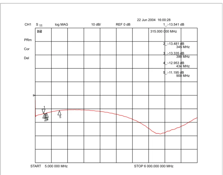
Application Note 38 Rev. 1.2, 2008-02-19
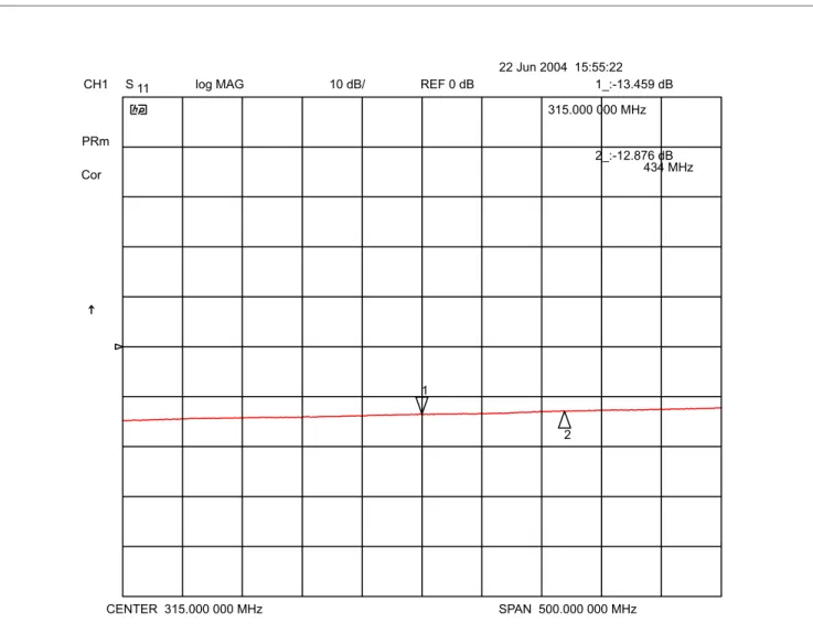
Input Return Loss, Log Mag, Narrow Span, Cascade = LNA + Bandpass Filter together
65 MHz - 565 MHz
Figure 29 Plot of Input Return Loss, Narrow Span, 315 MHz, Cascade
&+ 6 ORJ0$* G% 5()G% &(17(50+] 63$10+] &RU 35P -XQ BG% 0+] $1BSORWBLQSXWBUHWXUQBORVVBQDUURZBFDVFDGHBYVG
Application Note 39 Rev. 1.2, 2008-02-19
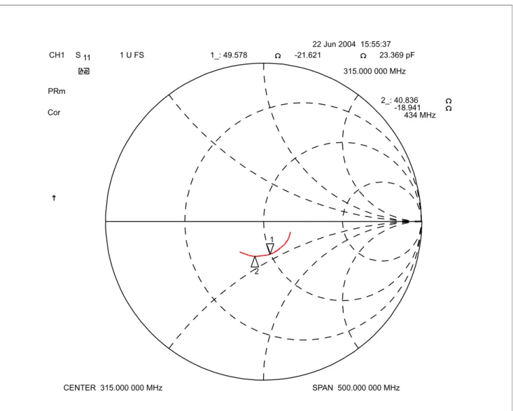
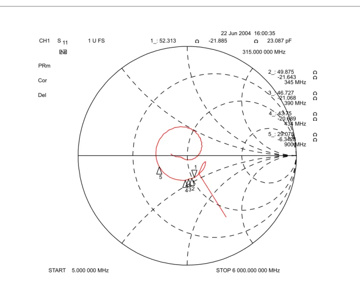
Input Return Loss, Smith Chart, Narrow Span, Cascade = LNA + Bandpass Filter together
Reference Plane = PCB Input SMA Connector 65 MHz - 565 MHz
Figure 30 Smith Chart of Input Return Loss, Narrow Span, 315 MHz, Cascade
&+ 6 8)6 &(17(50+] 63$10+] &RU 35P -XQ B S) 0+] $1BVPLWKBLQSXWBUHWXUQBORVVBQDUURZBFDVFDGHBYVG
Application Note 40 Rev. 1.2, 2008-02-19
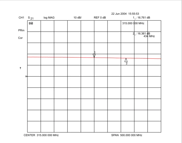
Forward Gain, Narrow Span, Cascade = LNA + Bandpass Filter together
65 MHz - 565 MHz
Note insertion gain of LNA + Bandpass Filter = 14.2 dB
Figure 31 Plot of Forward Gain, Narrow Span, 315 MHz, Cascade
&+ 6 ORJ0$* G% 5()G% &(17(50+] 63$10+] &RU 35P
0$5.(5
0+]
-XQ BG% 0+] BG% 0+] BG% 0+] BG% 0+] $1BSORWBIZBJDLQBQDUURZBFDVFDGHBYVGApplication Note 41 Rev. 1.2, 2008-02-19
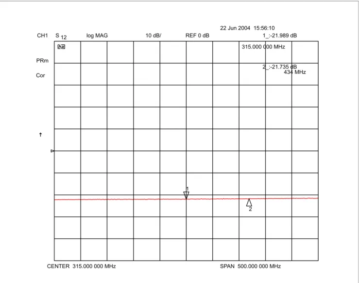
Reverse Isolation, Narrow Span, Cascade = LNA + Bandpass Filter together
65 MHz - 565 MHz
Note vertical scale is 20 dB / div
Figure 32 Plot of Reverse Isolation, Narrow Span, 315 MHz, Cascade
&+ 6 ORJ0$* G% 5()G% &(17(50+] 63$10+] &RU 35P
6&$/(
G%GLY
-XQ BG% 0+] BG% 0+] BG% 0+] BG% 0+] $1BSORWBUHYHUVHBLVRODWLRQBQDUURZBFDVFDGHBYVGApplication Note 42 Rev. 1.2, 2008-02-19
Output Return Loss, Log Mag, Narrow Span, Cascade = LNA + Bandpass Filter together
65 MHz - 565 MHz
Figure 33 Plot of Output Return Loss, Narrow Span, 315 MHz, Cascade
&+ 6 ORJ0$* G% 5()G% &(17(50+] 63$10+] &RU 35P
6&$/(
G%GLY
-XQ BG% 0+] BG% 0+] BG% 0+] BG% 0+] $1BSORWBRXWSXWBUHWXUQBORVVBQDUURZBFDVFDGHBYVGApplication Note 43 Rev. 1.2, 2008-02-19
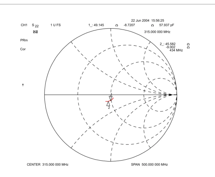
Output Return Loss, Smith Chart, Narrow Span, Cascade = LNA + Bandpass Filter together
Reference Plane = PCB Output SMA Connector 65 MHz - 565 MHz
Figure 34 Smith Chart of Output Return Loss, Narrow Span, 315 MHz, Cascade
&+ 6 8)6 &(17(50+] 63$10+] &RU 35P -XQ B S) 0+] B 0+] B 0+] B 0+] $1BVPLWKBRXWSXWBUHWXUQBORVVBQDUURZBFDVFDGHBYVG
Application Note 44 Rev. 1.2, 2008-02-19
Input Return Loss, Log Mag, Wide Sweep, Cascade = LNA + Bandpass Filter together
5 MHz - 6 GHz
Figure 35 Plot of Input Return Loss, Wide Sweep, 315 MHz, Cascade
&+ 6 ORJ0$* G% 5()G% 67$570+] 67230+] &RU 'HO 35P -XQ BG% 0+] BG% 0+] BG% 0+] BG% 0+] BG% 0+] $1BSORWBLQSXWBUHWXUQBORVVBZLGHBFDVFDGHBYVG
Application Note 45 Rev. 1.2, 2008-02-19
Forward Gain, Wide Sweep, Cascade = LNA + Bandpass Filter together
5 MHz - 6 GHz
Figure 36 Plot of Forward Gain, Wide Sweep, 315 MHz, Cascade
&+ 6 ORJ0$* G% 5()G% 67$570+] 67230+] &RU 'HO 35P
6&$/(
G%GLY
-XQ BG% 0+] BG% 0+] BG% 0+] BG% 0+] BG% 0+] $1BSORWBIZBJDLQBZLGHBFDVFDGHBYVGApplication Note 46 Rev. 1.2, 2008-02-19
Reverse Isolation, Wide Sweep, Cascade = LNA + Bandpass Filter together
5 MHz - 6 GHz
Figure 37 Plot of Reverse Isolation, Wide Sweep, 315 MHz, Cascade
&+ 6 ORJ0$* G% 5()G% 67$570+] 67230+] &RU 'HO 35P
6&$/(
G%GLY
-XQ BG% 0+] BG% 0+] BG% 0+] BG% 0+] BG% 0+] $1BSORWBUHYHUVHBLVRODWLRQBZLGHBFDVFDGHBYVGApplication Note 47 Rev. 1.2, 2008-02-19
Output Return Loss, Log Mag, Wide Sweep, Cascade = LNA + Bandpass Filter together
5 MHz - 6 GHz
Figure 38 Plot of Output Return Loss, Wide Sweep, 315 MHz, Cascade
&+ 6 ORJ0$* G% 5()G% 67$570+] 67230+] &RU 'HO 35P
6&$/(
G%GLY
-XQ BG% 0+] BG% 0+] BG% 0+] BG% 0+] BG% 0+] $1BSORWBRXWSXWBUHWXUQBORVVBZLGHBFDVFDGHBYVGApplication Note 48 Rev. 1.2, 2008-02-19
Appendix A. Measurement Results of a PCB showing filter re-tuned for 434 MHz Operation
For 434 MHz, LNA Section has no changes, and filter elements in filter section change as follows: • C3 and C9 change from 10 pF to 5.6 pF
• C7 changes from 5.6 pF to 2.7 pF • C6 and C8 change from 30 pF to 15 pF
Effort was made to maintain same coil type and value to simplify shift of filter passband from 315 to 434 MHz. Changes are to capacitor values only.
Summary of 434 MHz Bandpass Filter Data
T
= 25 °C, network analyzer source power = -30 dBmPlease refer to network analyzer plots of Bandpass Filter which appear later in this document.
Table 7 Summary of 434 MHz Bandpass Filter Data
Parameter Result Comments
Center Frequency 434 MHz Top-C Coupled Bandpass Filter, with 2 coils and 5 capacitors. Kept same coil values as values for 315 MHz filter shown earlier for convenience.
Insertion Loss 2.0 dB @ 434 MHz Insertion loss may be further optimized by using higher-Q chip coils. Coils used are low-cost versions and have Q values of approx. 35 at 300 MHz. Attenuation at 216 MHz, relative to
insertion loss at 315 MHz
54.7 dB Upper edge of Television Channel 13 in North America (potential “blocker” for 315 MHz receiver). See
Figure 25 and Figure 26. Attenuation at 470 MHz, relative to
insertion loss at 315 MHz
2.9 dB Lower edge of Television Channel 14 in North America. See Figure 25
and Figure 26. Input Return Loss 21.7 dB @ 434 MHz
Output Return Loss 25.6 dB @ 434 MHz Asymmetry between S11 and S22 due to PC board - refer to PCB scanned images.
Application Note 49 Rev. 1.2, 2008-02-19
Summary of Cascade (LNA + Bandpass Filter together) Data
T
= 25 °C, network analyzer source power = -30 dBmPlease refer to network analyzer screen-shots at end of this document to get a better idea of performance of LNA + Filter Cascade.
Table 8 Summary of Cascade Data, 434 MHz
Parameter Result Comments
Frequency Range 434 MHz Bandpass filter following LNA causes limitation of bandwidth. Filter may be re-tuned for other
frequencies of interest. DC Current 5.2 mA
DC Voltage,
V
CC 5.0 V 5.0 V standard in automotiveapplications
Collector-Emitter Voltage,
V
CE 3.1 V BFP460V
CE MAX= 4.5 V Gain 14.3 dB @ 434 MHzNoise Figure 1.6 dB @ 315 MHz These values do not extract PCB losses, etc. resulting from FR4 board an passives used on PCB - these results are at input SMA connector.
See Figure 5 and Table 6. Input Return Loss 13.3 dB @ 434 MHz
Output Return Loss 20.7 dB @ 434 MHz Reverse Isolation 23.5 dB @ 434 MHz
Application Note 50 Rev. 1.2, 2008-02-19
Bill of Material
Broadband BFP460 UHF Feedback LNA (Yellow shading) and Lumped-Element Top-C Coupled Bandpass Filter (Blue Shading), for 434 MHz variant
Table 9 Bill of Material for 434_MHz variant Reference
Designator
Value Manufacturer Case Size Function
C1 390 pF Various 0402 DC blocking, input.
C2 390 pF Various 0402 DC block for feedback network. C3 390 pF or
5.6 pF
Various 0402 For LNA alone, output DC block 390 pF. If bandpass filter is used, then C3 = 5.6 pF, serves as DC block & filter element. C4 0.1µF Various 0402 Decoupling, low frequency.
C5 390 pF Various 0402 Decoupling.
R1 110 kΩ Various 0402 DC bias for base of Q1. R2 560Ω Various 0402 Feedback resistor for LNA
R3 300Ω Various 0402 Bring DC to collector, high resistor values does not load LNA output.
R4 130Ω Various 0402 Provides some negative feedback for DC bias / DC operating point to compensate for variations in transistor DC current gain, temperature variations, etc. Also drops 5 V down to 4.4 V (below maximum collector-emitter voltage for BFP540F).
Q1 - Infineon Technologies SOT343 BFP460EHRT ESD-Robust Transistor (1500 V HBM).
f
T= 22 GHzJ1, J2, J3 - Johnson 142-0701-841 - RF input / output connectors J4 - AMP 5 pin header
MTA-100 series 640456-5 (standard pin plating) or 641215-5 (gold plated pins) - DC connector Pins 1, 5 = ground Pin 3 =
V
CC Pins 2, 4 = no connection L1, L2 5.6 nH Coilcraft 0402CS-5N6XJBU chip inductor0402 Coil for shunt resonators in bandpass filter.
C6, C8 15 pF Various 0402 Capacitor for shunt resonators in bandpass filter.
C7 2.7 pF Various 0402 Coupling cap between filter resonators. C9 5.6 pF Various 0402 Output cap of filter.
Application Note 51 Rev. 1.2, 2008-02-19
Schematic Diagram for UHF LNA and Optional 434 MHz Bandpass Filter
Note low parts count and simple design. No chip inductors are required for the LNA.
Figure 39 Schematic Diagram for UHF LNA and Optional 434 MHz Bandpass Filter
$1B6FKHPDWLFBYVG 3&% 5HY% 3&%RDUG0DWHULDO 6WDQGDUG)5 4 %)3(+57 7UDQVLVWRU -5),1387 & S) , P$QRPLQDO 5 . & S) 5 RKPV & X) 9FF 9 -'&&RQQHFWRU -5)287387 & S)S) 5 RKPV & S) 5 RKPV -5),1387 287387 & S) & S) 1RWHV %ODFNUHFWDQJOHVDUHRKPPLFURVWULSWUDFNV &VHUYHVWZRSXUSRVHV'&EORFNDQGRU%DQGSDVV)LOWHUHOHPHQW ZKHQWHVWLQJ/1$DORQH&LVD'&EORFNDQGVZLQJ&S)GRZQ FORFNZLVHDWDGHJUHHDQJOHIURP/1$RXWSXWWRPDNH-WKH5)RXWSXW :KHQ%DQGSDVVILOWHUDORQHLVWREHWHVWHG&FKDQJHVWRS)DQG& EULGJHVJDSEHWZHHQWUDFHIURP-DQGWUDFNIRUILOWHUWRULJKWXSDW GHJUHHDQJOH :KHQFDVDFDGHRI/1$)LOWHULVWREHWHVWHG& S)EXW&LV SODFHGVWUDLJKWDFURVVIURP/1$RXWSXWWRLQSXWRIILOWHUVHFWLRQ / Q+ & S) / Q+ 0+]7RS&&RXSOHG %DQGSDVV)LOWHU %)3:LGHEDQG)HHGEDFN/1$ RKPWUDFH RKPWUDFH RKPWUDFH RKPWUDFH & S)
Application Note 52 Rev. 1.2, 2008-02-19
Noise Figure, Plot, Cascade of LNA + BPF, Center of Plot (x-axis) is 434 MHz.
Figure 40 Noise Figure of Cascade @ 434 MHz
$1BSORWBQIB&DVFDGHBYVG 5RKGH 6FKZDU])6(. 1RLVH)LJXUH/1$0+]%DQGSDVV)LOWHU $XJ (871DPH %)3%URDGEDQG8+))HHGEDFN/1$SOXV0+]/&%DQGSDVV)LOWHU 0DQXIDFWXUHU ,QILQHRQ7HFKQRORJLHV 2SHUDWLQJ&RQGLWLRQV 9 97 & 2SHUDWRU1DPH *HUDUG:HYHUV 7HVW6SHFLILFDWLRQ /:56'/1$35HYLVLRQ) &RPPHQW 3&%5HY% $XJ $QDO\]HU 5)$WW G% 5HI/YO G%P 5%: 0+] 9%: +] 5DQJH G% 5HI/YODXWR 21 0HDVXUHPHQW QGVWDJHFRUU 21 0RGH 'LUHFW (15 +3$(15 0+] 0+]',9 0+] 1RLVH)LJXUHG%
Application Note 53 Rev. 1.2, 2008-02-19
Noise Figure, Cascade of LNA + 434 MHz Bandpass Filter, Tabular Data
From Rohde & Schwarz FSEK3 + FSEM30
Table 10 Noise Figure, Cascade @ 434 MHz
Frequency Noise Figure
383.92 MHz 1.87 dB 388.92 MHz 1.82 dB 393.92 MHz 1.74 dB 403.92 MHz 1.70 dB 408.92 MHz 1.67 dB 413.92 MHz 1.65 dB 418.92 MHz 1.60 dB 423.92 MHz 1.63 dB 428.92 MHz 1.62 dB 433.92 MHz 1.61 dB 438.92 MHz 1.62 dB 443.92 MHz 1.62 dB 448.92 MHz 1.59 dB 453.92 MHz 1.60 dB 458.92 MHz 1.60 dB 463.92 MHz 1.61 dB 468.92 MHz 1.64 dB 473.92 MHz 1.61 dB 478.92 MHz 1.64 dB 483.92 MHz 1.63 dB
Application Note 54 Rev. 1.2, 2008-02-19
Input Return Loss, Log Mag, Narrow Span, 434 MHz Bandpass Filter alone
84 MHz - 784 MHz
Figure 41 Plot of Input Return Loss, Narrow Span, 434 MHz BPF alone
&+ 6 ORJ0$* G% 5()G% &(17(50+] 63$10+] &RU 'HO 35P $XJ BG% 0+] BG% 0+] BG% 0+] BG% 0+] $1BSORWBLQSXWBUHWXUQBORVVBQDUURZB%3)BYVG
Application Note 55 Rev. 1.2, 2008-02-19
Input Return Loss, Smith Chart, Narrow Span, 434 MHz Bandpass Filter alone
Reference Plane = PCB Input SMA Connector 84 MHz - 784 MHz
Figure 42 Smith Chart of Input Return Loss, Narrow Span, 434 MHz, BPF alone
&+ 6 8)6 &(17(50+] 63$10+] &RU 'HO 35P $XJ B S) 0+] BP 0+] B 0+] B 0+] $1BVPLWKBLQSXWBUHWXUQBORVVBQDUURZB%3)BYVG
Application Note 56 Rev. 1.2, 2008-02-19
Insertion Loss, Narrow Span, 434 MHz Bandpass Filter alone
84 MHz - 784 MHz
Note Insertion Loss is appro. 2.0 dB @ 433.92 MHz
Figure 43 Plot of Insertion Loss, Narrow Span, 434 MHz BPF alone
&+ 6 ORJ0$* G% 5()G% &(17(50+] 63$10+] &RU 6PR 'HO 35P $XJ BG% 0+] BG% 0+] BG% 0+] BG% 0+] $1BSORWBLQVHUWLRQBORVVBQDUURZB%3)BYVG
Application Note 57 Rev. 1.2, 2008-02-19
Insertion Loss, Wide Span, 434 MHz Bandpass Filter alone
5 MHz - 6 GHz
Note suppression at North American FM Broadcast Band (e.g. 108 MHz), TV Broadcast Channel 13 (210 - 216 MHz), TV Channel 14 (470 - 476 MHz), Cellular Tx (≅900 MHz) and PCS Tx (≅1900 MHz)
Figure 44 Plot of Insertion Loss, Wide Span, 434 MHz BPF alone
&+ 6 ORJ0$* G% 5()G% 67$570+] 67230+] &RU 'HO 35P $XJ BG% 0+] BG% 0+] BG% 0+] BG% 0+] BG% 0+] $1BSORWBLQVHUWLRQBORVVBZLGHB%3)BYVG
Application Note 58 Rev. 1.2, 2008-02-19
Output Return Loss, Log Mag, Narrow Span, 434 MHz Bandpass Filter alone
84 MHz - 784 MHz
Figure 45 Plot of Output Return Loss, Narrow Span, 434 MHz BPF alone
&+ 6 ORJ0$* G% 5()G% &(17(50+] 63$10+] &RU 6PR 'HO 35P $XJ BG% 0+] BG% 0+] BG% 0+] BG% 0+] $1BSORWBRXWSXWBUHWXUQBORVVBQDUURZB%3)BYVG
Application Note 59 Rev. 1.2, 2008-02-19
Output Return Loss, Smith Chart, Narrow Span, 434 MHz Bandpass Filter alone
Reference Plane = PCB Output SMA Connector 84 MHz - 784 MHz
Figure 46 Smith Chart of Output Return Loss, Narrow Span, 434 MHz BPF alone
&+ 6 8)6 &(17(50+] 63$10+] &RU 6PR 'HO 35P $XJ B S) 0+] BP 0+] B 0+] B 0+] $1BVPLWKBRXWSXWBUHWXUQBORVVBQDUURZB%3)BYVG
Application Note 60 Rev. 1.2, 2008-02-19
Input Return Loss, Log Mag, Narrow Span, Cascade = LNA + Bandpass Filter together
84 MHz - 784 MHz
Figure 47 Plot of Input Return Loss, Narrow Span, 434 MHz, Cascade
&+ 6 ORJ0$* G% 5()G% &(17(50+] 63$10+] &RU 6PR 'HO 35P $XJ BG% 0+] BG% 0+] BG% 0+] BG% 0+] $1BSORWBLQSXWBUHWXUQBORVVBQDUURZBFDVFDGHBYVG
Application Note 61 Rev. 1.2, 2008-02-19
Input Return Loss, Smith Chart, Narrow Span, Cascade = LNA + Bandpass Filter together
Reference Plane = PCB Input SMA Connector 84 MHz - 784 MHz
Figure 48 Smith Chart of Input Return Loss, Narrow Span, 434 MHz, Cascade
&+ 6 8)6 &(17(50+] 63$10+] &RU 6PR 'HO 35P $XJ B S) 0+] B 0+] B 0+] B 0+] $1BVPLWKBLQSXWBUHWXUQBORVVBQDUURZBFDVFDGHBYVG
Application Note 62 Rev. 1.2, 2008-02-19
Forward Gain, Narrow Span, Cascade = LNA + Bandpass Filter together
84 MHz - 784 MHz
Note insertion gain of LNA + Bandpass filter = 14.3 dB
Figure 49 Plot of Forward Gain, Narrow Span, 434 MHz, Cascade
&+ 6 ORJ0$* G% 5()G% &(17(50+] 63$10+] &RU 6PR 'HO 35P
6&$/(
G%GLY
$XJ BG% 0+] BG% 0+] BG% 0+] BG% 0+] $1BSORWBIZBJDLQBQDUURZBFDVFDGHBYVGApplication Note 63 Rev. 1.2, 2008-02-19
Reverse Isolation, Narrow Span, Cascade = LNA + Bandpass Filter together
84 MHz - 784 MHz
Figure 50 Plot of Reverse Isolation, Narrow Span, 434 MHz, Cascade
&+ 6 ORJ0$* G% 5()G% &(17(50+] 63$10+] &RU 6PR 'HO 35P $XJ BG% 0+] BG% 0+] BG% 0+] BG% 0+] $1BSORWBUHYHUVHBLVRODWLRQBQDUURZBFDVFDGHBYVG
Application Note 64 Rev. 1.2, 2008-02-19
Output Return Loss, Log Mag, Narrow Span, Cascade = LNA + Bandpass Filter together
84 MHz - 784 MHz
Figure 51 Plot of Output Return Loss, Narrow Span, 434 MHz, Cascade
&+ 6 ORJ0$* G% 5()G% &(17(50+] 63$10+] &RU 6PR 'HO 35P $XJ BG% 0+] BG% 0+] BG% 0+] BG% 0+] $1BSORWBRXWSXWBUHWXUQBORVVBQDUURZBFDVFDGHBYVG
Application Note 65 Rev. 1.2, 2008-02-19
Output Return Loss, Smith Chart, Narrow Span, Cascade = LNA + Bandpass Filter together
Reference Plane = PCB Output SMA Connector 84 MHz - 784 MHz
Figure 52 Smith Chart of Output Return Loss, Narrow Span, 434 MHz, Cascade
&+ 6 8)6 &(17(50+] 63$10+] &RU 6PR 'HO 35P $XJ B S) 0+] BP 0+] B 0+] B 0+] $1BVPLWKBRXWSXWBUHWXUQBORVVBQDUURZBFDVFDGHBYVG
Application Note 66 Rev. 1.2, 2008-02-19
Input Return Loss, Log Mag, Wide Sweep, Cascade = LNA + Bandpass Filter together
5 MHz - 6 GHz
Figure 53 Plot of Input Return Loss, Wide Sweep, 434 MHz, Cascade
&+ 6 ORJ0$* G% 5()G% 67$570+] 67230+] &RU 'HO 35P $XJ BG% 0+] BG% 0+] BG% 0+] BG% 0+] BG% 0+] $1BSORWBLQSXWBUHWXUQBORVVBZLGHBFDVFDGHBYVG
Application Note 67 Rev. 1.2, 2008-02-19
Forward Gain, Wide Sweep, Cascade = LNA + Bandpass Filter together
5 MHz - 6 GHz
Figure 54 Plot of Forward Gain, Wide Sweep, 434 MHz, Cascade
&+ 6 ORJ0$* G% 5()G% 67$570+] 67230+] &RU 'HO 35P $XJ BG% 0+] BG% 0+] BG% 0+] BG% 0+] BG% 0+] $1BSORWBIZBJDLQBZLGHBFDVFDGHBYVG
Application Note 68 Rev. 1.2, 2008-02-19
Reverse Isolation, Wide Sweep, Cascade = LNA + Bandpass Filter together
5 MHz - 6 GHz
Figure 55 Plot of Reverse Isolation, Wide Sweep, 434 MHz, Cascade
&+ 6 ORJ0$* G% 5()G% 67$570+] 67230+] &RU 'HO 35P $XJ BG% 0+] BG% 0+] BG% 0+] BG% 0+] BG% 0+] $1BSORWBUHYHUVHBLVRODWLRQBZLGHBFDVFDGHBYVG
Application Note 69 Rev. 1.2, 2008-02-19
Output Return Loss, Log Mag, Wide Sweep, Cascade = LNA + Bandpass Filter together
5 MHz - 6 GHz
Figure 56 Plot of Output Return Loss, Wide Sweep, 434 MHz, Cascade
&+ 6 ORJ0$* G% 5()G% 67$570+] 67230+] &RU 'HO 35P