General Description
The MAX5440 dual, 40k
Ω
logarithmic taper volume
con-trol features a debounced up/down interface for use
with a simple rotary encoder without using a
microcon-troller (µC). Each potentiometer has 32 log-spaced tap
points with a buffered wiper output and replaces
mechanical potentiometers. An integrated bias
genera-tor provides the required ((V
DD+ V
SS) / 2) bias voltage,
eliminating the need for costly external op-amp circuits
in unipolar audio applications. A mode-indicator LED
output specifies volume or balance control. Five
inte-grated LED drivers indicate volume level or balance
set-tings, depending on the status of the mode indicator.
The MAX5440 includes debounced pushbutton inputs
for mute and mode. The mute input allows a single
pushbutton to change between volume control and the
-90dB (typ) mute setting. The mode input toggles
between volume and balance control. A click-and-pop
suppression feature minimizes the audible noise
gener-ated by wiper transitions. The MAX5440 provides a
nominal temperature coefficient of 35ppm/°C
end-to-end and 5ppm/°C, ratiometrically. The MAX5440 is
available in a 24-pin SSOP package and is specified for
operation over the -40°C to +85°C extended
tempera-ture range.
Applications
Stereo Volume Control
Desktop Speakers
Multimedia Docking Stations
Set-Top Boxes
Automotive Back-Seat Multimedia
Features
♦
Logarithmic Taper Volume Control with (31) 2dB
Steps
♦
Low-Power Wiper Buffers Provide 0.003% THD
♦
Single +2.7V to +5.5V or Dual ±2.7V Supply
Voltage Operation
♦
Low 0.5µA Shutdown Supply Current
♦
Integrated Bias Voltage Generator
♦
Five-Segment LED Volume/Balance Indicator
♦
Clickless Switching
♦
40k
Ω
End-to-End Fixed Resistance Value
♦
Mute Function Toggles to -90dB (typ)
♦
Power-On Reset to -12dBFS Wiper Position
MAX5440
with Rotary Encoder Interface
________________________________________________________________Maxim Integrated Products 1
24 23 22 21 20 19 17 1 2 3 4 5 6 8 GND MODEIND LEDIND4 LEDIND3 VLOGIC VSS VDD MUTE RENCODEB RENCODEA TOP VIEW MAX5440 LEDIND2 LEDIND1 H1 H0 SHDN 18 7 LEDIND0 GND 15 10 W1 W0 16 9 L1 L0 13 12 BIAS 14 11 MIDBIAS MODE SSOP
Pin Configuration
VDD VSS (VDD + VSS) / 2 (VDD + VSS) / 2 VLOGIC VPEAK H1 L1 W1 SHDN LEFT INPUT RIGHT INPUT MODEIND HEADPHONE DRIVER L0 H0 W0 VLOGIC LEDIND4 LEDIND3 LEDIND0GND MUTE MODE RENCODEA RENCODEA
LEDIND1 LEDIND2 ROTARY ENCODER MIDBIAS BIAS MAX5440
Typical Operating Circuit
Ordering Information
PART TEMP RANGE PIN-PACKAGE PKG
CODE
MAX5440EAG -40°C to +85°C 24 SSOP A24-1
MAX5440
ABSOLUTE MAXIMUM RATINGS
Stresses beyond those listed under “Absolute Maximum Ratings” may cause permanent damage to the device. These are stress ratings only, and functional operation of the device at these or any other conditions beyond those indicated in the operational sections of the specifications is not implied. Exposure to absolute maximum rating conditions for extended periods may affect device reliability.
SHDN, MUTE, RENCODEA, RENCODEB,
and MODEto GND...-0.3V to (VLOGIC+ 0.3V)
H_, L_, and W_ to VSS ...-0.3V to (VDD+ 0.3V)
LEDIND_, MODEINDto GND...-0.3V to (VLOGIC+ 0.3V)
MIDBIAS, BIAS to VSS...(VSS- 0.3V) to (VDD+ 0.3V)
VLOGICto GND...-0.3V to (VDD+ 0.3V)
VDDto GND ...-0.3V to +6V
VDDto VSS...-0.3V to +6V
VSSto GND...-3V to +0.3V
Input and Output Latchup Immunity...±200mA Continuous Power Dissipation (TA= +70°C)
24-Pin SSOP (derate 8mW/°C above +70°C) ...640mW Operating Temperature Range ...-40°C to +85°C Junction Temperature ...+150°C Storage Temperature Range ...-60°C to +150°C Lead Temperature (soldering, 10s) ...+300°C
ELECTRICAL CHARACTERISTICS
(VDD= +2.7V to +5.5V, VSS= GND = 0, 2.7V ≤(VDD- VSS) ≤5.5V, VLOGIC= +2.7V to VDD, VH_ = VDD, VL_ = VDD/ 2, TA= TMINto
TMAX, unless otherwise specified. Typical values are at TA= +25°C.) (Note 1)
PARAMETER SYMBOL CONDITIONS MIN TYP MAX UNITS
End-to-End Resistance R 36 40 52 kΩ Absolute Tolerance ±0.25 dB Tap-to-Tap Tolerance ±0.1 dB V H _= ( V D D / 2) + 1V RM S , 1kH z tap at top , RL = ∞ to V L_ = V D D / 2, 20H z to 20kH z 0.004 V H _= ( V D D / 2) + 1.5V RM S , 1kH z tap at top , RL = ∞ to V L_ = V D D / 2, 20H z to 20kH z 0.006 VDD = 5V,VSS = 0V, V L_ = 1.5V, VH_ = (VDD / 2) + 1VRMS, 1kHz tap at top, RL = 10kΩ to VMIDBIAS, 20Hz to 20kHz 0.004 Total Harmonic Distortion Plus
Noise THD+N VDD = 5V,VSS = 0V, V L_ = 5V, V H _= ( V D D / 2) + 1.5V RM S , 1kHz tap at top, RL = 10kΩ to VMIDBIAS, 20Hz to 20kHz 0.006 % Channel Isolation 100 dB Interchannel Matching ±0.5 dB Mute Attenuation SHDN = VDD 90 dB
Power-Supply Rejection Ratio PSRR Input referred, 217Hz, 100mVP-P on VDD -60 dB
H Terminal Capacitance CH 5 pF L Terminal Capacitance CL 7 pF End-to-End Resistance 35 ppm/°C Ratiometric Resistance 5 ppm/°C Bandwidth, -3dB fCUTOFF CW = 33pF 100 kHz Output Noise en 20Hz to 20kHz 3.2 µVRMS WIPER BUFFER
Output Voltage Swing VO RL = 10kΩ to VMIDBIAS VDD - 0.2 V
Output Current 3 mA
Output Resistance ROWB 1 10 Ω
DC Offset -5 ±2 +5 mV
INTEGRATED BIAS GENERATOR
Output Voltage ILOAD = 1mA
(VDD + VSS) / 2 - 10mV (VDD + VSS) / 2 ( V D D + V S S ) / 2 + 10m V V
MAX5440
ELECTRICAL CHARACTERISTICS (continued)
(VDD= +2.7V to +5.5V, VSS= GND = 0, 2.7V ≤(VDD- VSS) ≤5.5V, VLOGIC= +2.7V to VDD, VH_ = VDD, VL_ = VDD/ 2, TA= TMINto
TMAX, unless otherwise specified. Typical values are at TA= +25°C.) (Note 1)
PARAMETER SYMBOL CONDITIONS MIN TYP MAX UNITS
Power-Supply Rejection Ratio PSRRBR 1kHz, 100mV on VDD, 1µF on BIAS 60 dB
Maximum Load To VDD or GND 3 kΩ
Output Resistance ROBR 6 Ω
CONTACT INPUTS (MUTE, MODE, RENCODEA, RENCODEB)
Internal Pullup Resistor RPULLUP 45 kΩ
Single Pulse Input Low Time tCPW 22 ms
Repetitive Input Pulse Separation tIPWS 50 ms
Timeout Period tWS Click/pop suppression inactive 32 ms
DIGITAL INPUTS (MUTE, MODE, RENCODEA, RENCODEB, SHDN)
3.6V < VLOGIC ≤ 5.5V 2.4
Input High Voltage (Note 2) VIH
2.7V ≤ VLOGIC ≤ 3.6V 2.0
V
3.6V < VLOGIC ≤ 5.5V 0.8
Input Low Voltage (Note 2) VIL
2.7V ≤ VLOGIC ≤ 3.6V 0.6
V
Input Leakage Current Inputs unconnected -1 +1 µA
Input Capacitance 5 pF
POWER SUPPLIES
Supply Voltage VDD VSS = 0 2.7 5.5 V
Negative Power Supply VSS VDD = +2.7V -2.7 0 V
Supply Voltage Difference VDD - VSS 5.5 V
Active Supply Current IDD 1.4 mA
VDD = +5V, VSS = 0 1.3
S tand b y S up p l y C ur r ent ( N otes 3, 4) ISTBY
VDD = +2.7V, VSS = -2.7V 1.3
mA
Shutdown Supply Current ISHDN (Note 3) 1 µA
Power-Up Time tPU Click/pop suppression inactive 50 ms
Logic Supply Voltage VLOGIC VSS = 0 2.7 VDD V
Logic Active Supply Current IL VRENCODEA = VRENCODEB= 0V 320 µA
Logic Standby Supply Current ILSTBY (Note 4) 1 µA
Logic Shutdown Current ILSHDN 1 µA
LED INDICATORS (LEDIND0–LEDIND4, MODEIND)
VLOGIC = 2.7V, ISINK = 10mA 0.4
Output Low Voltage VOL
VLOGIC = 5.5V, ISINK = 10mA 0.2
V
Output Leakage Current 0.1 10 µA
Output Capacitance 3 pF
Maximum Sink Current 150 mA
Note 1:Parameters are 100% production tested at +85°C and limits through temperature are guaranteed by design.
Note 2:The device draws current in excess of the specified supply current when the digital inputs are driven with voltages between
(VDD- 0.5V) and (GND + 0.5V). See Digital Supply Current vs. Digital Input Voltage in the Typical Operating Characteristics.
Note 3:Shutdown refers to the SHDNinput being asserted low. Standby refers to SHDNnot being asserted and all I/O inactive. Note 4:Supply current measured with the wiper position fixed.
MAX5440
Typical Operating Characteristics
(TA = +25°C, unless otherwise noted.)-70 -60 -40 -50 -20 -10 -30 0 0 4 8 12 16 20 24 28 32 ATTENUATION vs. TAP POSITION
MAX5440 toc01 TAP POSITION ATTENUATION (dB) -0.25 -0.15 -0.20 -0.05 -0.10 0.05 0 0.10 -40 -15 10 35 60 85 END-TO-END RESISTANCE % CHANGE
vs. TEMPERATURE
MAX5440 toc02
TEMPERATURE (°C)
END-TO-END RESISTANCE CHANGE (%)
1.38 1.41 1.40 1.39 1.42 1.43 1.44 1.45 1.46 1.47 1.48 -40 -15 10 35 60 85 TOTAL SUPPLY CURRENT
vs. TEMPERATURE
MAX5440 toc03
TEMPERATURE (°C)
TOTAL SUPPLY CURRENT (mA)
VLOGIC = VDD = 5.5V WIPER TRANSITION FROM -2dB TO -4dB 20ms/div
WIPER SWITCHING TRANSIENT
MAX5440 toc04 RENCODEA RENCODEB 51ms 0 20 10 40 30 60 50 70 90 80 100 0 4 8 12 16 20 24 28 32 WIPER-TO-END TERMINAL VOLTAGE
vs. TAP POSITION
MAX5440 toc05
TAP POSITION
NOMINAL END-TO-END VOLTAGE (%V
HL ) VHW VWL -2.8 -2.0 -2.4 -0.4 -0.8 -1.2 -1.6 0.8 0.4 0 0.01 0.1 1 10 100 1000 FREQUENCY RESPONSE MAX5440 toc06 FREQUENCY (kHz) RESPONSE (dB) VH_ = 2.5 ±1VRMS, VL_ = 2.5V, CL_ = 33pF W_ SET TO 0dB -8.8 -8.0 -8.4 -6.4 -6.8 -7.6 -7.2 -5.6 -6.0 -5.2 0.01 0.1 1 10 100 1000 FREQUENCY RESPONSE MAX5440 toc07 FREQUENCY (kHz) RESPONSE (dB) W_ SET TO -6dB VH_ = 2.5 ±1VRMS, VL_ = 2.5V, CL_ = 33pF 0.001 0.01 0.1 0.001 0.01 0.1 1 10 100 THD+N vs. FREQUENCY MAX5440 toc08 FREQUENCY (kHz) W_ SET AT -2dB THD+N (%) VDD = 2.5V VSS = -2.5V L_ = VMIDBIAS H_ = VMIDBIAS + 1VRMS W_ SET AT -6dB W_ SET AT 0dB 0.001 0.01 0.1 0.001 0.01 0.1 1 10 100 THD+N vs. FREQUENCY MAX5440 toc09 FREQUENCY (kHz) THD+N (%) VDD = 5.0V VSS = GND L_ = VMIDBIAS H_ = VMIDBIAS + 1VRMS W_ SET AT -2dB W_ SET AT -6dB W_ SET AT 0dB
MAX5440
-75 -65 -70 -45 -50 -55 -60 -35 -40 -25 -30 0.01 0.1 1 10 100 POWER-SUPPLY REJECTION RATIOvs. FREQUENCY MAX5440 toc10 FREQUENCY (kHz) RESPONSE (dB) VDD_ = 5V ±100mVP-P, VH = 5V VL_ = 2.5V, W_ SET TO -6dB 0 100 50 200 150 250 300
LOGIC SUPPLY CURRENT vs. LOGIC SUPPLY VOLTAGE
MAX5440 toc11
LOGIC SUPPLY VOLTAGE (V)
LOGIC SUPPLY CURRENT (
µ A) 2.5 3.0 3.5 4.0 4.5 5.0 5.5 ACTIVE CURRENT STANDBY CURRENT SHUTDOWN 0 100 50 200 150 300 250 350 -40 -15 10 35 60 85 ACTIVE LOGIC SUPPLY CURRENT
vs. TEMPERATURE
MAX5440 toc12
TEMPERATURE (°C)
LOGIC SUPPLY CURRENT (
µ A) VDD = VLOGIC = 5.5V, RENCODEA = RENCODEB = 0 1.1752 1.1756 1.1754 1.1762 1.1760 1.1758 1.1768 1.1766 1.1764 1.1770 -40 -15 10 35 60 85 ACTIVE SUPPLY CURRENT
vs. TEMPERATURE
MAX5440 toc13
TEMPERATURE (°C)
SUPPLY CURRENT (mA)
VDD = VLOGIC = 5.5V, RENCODEA = RENCODEB = 0 10 100 1000 0 0.5 1.0 1.5 2.0 2.5 3.0 3.5 4.0 4.5 5.0 DIGITAL SUPPLY CURRENT vs. DIGITAL INPUT VOLTAGE
MAX5440 toc14
DIGITAL INPUT VOLTAGE (V)
DIGITAL SUPPLY CURRENT (
µ A) 200 0 400 800 600 1000 1200 0.01 0.1 1 10 100 SPECTRAL NOISE DENSITY
MAX5440 toc15 FREQUENCY (kHz) NOISE (nV/ √ Hz) 0 1 2 3 4 5 6 7 8 2.5 3.0 3.5 4.0 4.5 5.0 SUPPLY CURRENT
vs. INPUT VOLTAGE SWEEP
MAX5440 toc16
INPUT VOLTAGE SWEEP (VH_)
SUPPLY CURRENT (mA)
VDD = VLOGIC = 5V, W_ AT 0dB
RL = 10kΩ TO VMIDBIAS
Typical Operating Characteristics (continued)
MAX5440
PIN NAME FUNCTION
1 VLOGIC Digital Logic Power Supply. Bypass VLOGIC to ground with a 0.1µF capacitor as close to the device
as possible.
2 RENCODEA Rotary Encoder Input A. With RENCODEB, this input provides the rotary encoder control for the
potentiometer (see Figure 1). RENCODEA is internally pulled up to VLOGIC with a 45kΩ resistor.
3 RENCODEB Rotary Encoder Input B. With RENCODEA, this input provides the rotary encoder control for the
potentiometer (see Figure 1). RENCODEB is internally pulled up to VLOGIC with a 45kΩ resistor.
4 MUTE Mute Input. Pull MUTE low to toggle the wiper between the mute setting (see Table 1) and the current
setting. MUTE is pulled up to VLOGIC with an internal 45kΩ resistor.
5 MODE
Volume/Balance Control Input. Each high-to-low transition on MODE toggles between the volume and
balance modes. MODE is pulled high internally with a 45kΩ resistor to VLOGIC. On power-up, the
MAX5440 is in volume-control mode.
6 SHDN
Active-Low Shutdown Input. Drive SHDN low to place the device in shutdown mode. In shutdown
mode, the MAX5440 stores the last wipers settings. The wipers move to the L_ end of the resistor string. Terminating shutdown mode restores the wipers to their previous settings.
7, 24 GND Ground. Connect pins 7 and 24 together.
8 H0 Potentiometer 0 High Terminal. H0 and L0 terminals can be reversed.
9 L0 Potentiometer 0 Low Terminal. L0 and H0 terminals can be reversed.
10 W0 Potentiometer 0 Wiper Buffered Output
11 MIDBIAS Midbias Voltage Output. VMIDBIAS = (VDD + VSS) / 2.
12 BIAS Bias Generator Input. Bypass with a 1µF capacitor to system ground.
13 VDD Analog Power Supply. Bypass VDD to ground with a 0.1µF capacitor as close to the device as
possible.
14 VSS Negative Power Supply. Bypass VSS to ground with a 0.1µF capacitor as close to the device as
possible. Connect to GND for single-supply operation.
15 W1 Potentiometer 1 Wiper Buffered Output
16 L1 Potentiometer 1 Low Terminal. L1 and H1 terminals can be reversed.
17 H1 Potentiometer 1 High Terminal. H1 and L1 terminals can be reversed.
18–22 LEDIND0–
LEDIND4
LE D Ind i cator O p en- D r ai n Outp ut 0 thr oug h LE D Ind i cator O p en- D r ai n Outp ut 4. LE D IN D 0–LE D IN D 4 for m a b ar g r ap h i nd i cati on of the cur r ent vol um e or b al ance. In vol um e m od e, al l LE D s off i nd i cates m ute and al l LE D s on i nd i cates m axi m um vol um e. In b al anced m od e, LE D 2 on i nd i cates center ed or b al anced .
23 MODEIND
Volume-Control/Balance-Control Mode Indicator Open-Drain Output. Connect to an LED through a
resistor to VLOGIC. When the LED is on, the MAX5440 is in balance-control mode. When the LED is
off, the MAX5440 is in volume-control mode.
MAX5440
Detailed Description
The MAX5440 dual, 40k
Ω
logarithmic taper digital
potentiometer features a debounced up/down interface
for use with a simple rotary encoder without using a
microcontroller. Each potentiometer has 32 log-spaced
tap points with a buffered wiper output and replaces
mechanical potentiometers.
Mode Control (
MODE
)
The MAX5440
MODE
input toggles between volume
and balance modes. Force
MODE
low to toggle
between volume and balance modes. For example,
dri-ving
MODE
low once while in volume-control mode
switches the MAX5440 to balance mode. Driving
MODE
low again switches the MAX5440 back to volume mode.
MODE
is internally pulled high with a 45k
Ω
resistor to
V
LOGIC. The MAX5440 powers up in volume-control
mode. Leave unconnected or connect to V
LOGICif
bal-ance mode is not required.
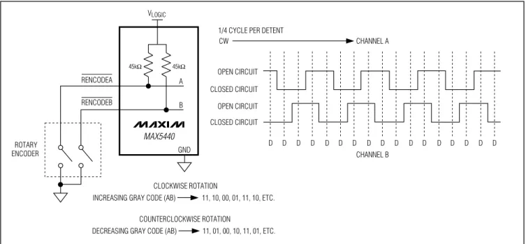
Rotary Encoder Interface
The MAX5440 interfaces with rotary encoder switches.
The rotary encoder is a contact closure type switch with
two outputs that connect to
RENCODEA
and
RENCODEB
on the device. As the shaft is rotated,
RENCODEA
and
RENCODEB
produce a gray code
count. Figure 1 shows a typical rotary encoder interface.
State changes trigger a wiper movement and the
direc-tion of the count dictates the direcdirec-tion of wiper
move-ment. An increasing gray code count moves the wiper
up to a lower attenuation setting in volume mode and
towards a full right channel (CH1) in balance mode. A
decreasing gray code count moves the wiper down to a
higher attenuation in volume mode and towards a full left
channel (CH0) in balance mode. Both switch inputs are
internally pulled up to V
LOGICby internal 45k
Ω
resistors.
During rapid rotation, the inputs must be stable for at
least 20ms and have separation between state
changes by at least 40ms for the debounce circuitry to
accurately detect the input states.
Figure 1. Rotary Encoder Interface
MAX5440 B RENCODEA RENCODEB ROTARY ENCODER A GND VLOGIC 45kΩ 45kΩ CLOCKWISE ROTATION
INCREASING GRAY CODE (AB) 11, 10, 00, 01, 11, 10, ETC.
COUNTERCLOCKWISE ROTATION
DECREASING GRAY CODE (AB) 11, 01, 00, 10, 11, 01, ETC. CW CLOSED CIRCUIT OPEN CIRCUIT OPEN CIRCUIT CLOSED CIRCUIT CHANNEL A CHANNEL B 1/4 CYCLE PER DETENT
MAX5440
W0 H_ L_ H_ L_ H_ L_ H_ L_ W1 W0 ROTATE CW TWICE ROTATE CCW ONCE BALANCE SEPARATION MAINTAINED NO CHANGEORIGINAL BALANCE SEPARATION MAINTAINED ROTATE CW ROTATE CCW ROTATE CW ONCE ROTATE CW ONCE ROTATE CCW ONCE ROTATE CW ONCE FROM C TO D W1 W0 W1 W0 W1 W0 W1 W0 W1 W0 W1 W0 W1 W0 W1 W0 W1 W0 W1 W0 W1 a b c d
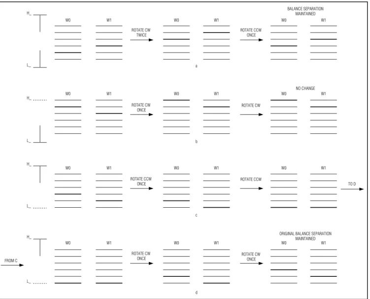
Volume Control
In volume-control mode, the MAX5440’s wipers move
simultaneously, maintaining the balance separation
between each wiper (Figure 2a).
When either wiper reaches the maximum tap position
(position closest to H_), further commands to increase
the volume are ignored. Balance separation is
main-tained in the maximum volume configuration (Figure 2b).
When either wiper reaches the minimum tap position
(position closest to L_), further commands to decrease
the volume adjust the other wiper until it also reaches
the minimum tap position (Figure 2c).
Increasing the volume from this minimum position
restores the original balance separation of the wipers
(Figure 2d).
When both wipers are in the tap 31 position (-62dB
attenuation), further decreasing rotations place the
wipers in the mute position (see Table 1). Rotating the
encoder to a lower attenuation or a pulse to
MUTE
returns the wipers to tap 31.
Balance Control
In balance-control mode, the MAX5440 adjusts the
bal-ance between channel 0 and channel 1 while
maintain-ing the set volume. For example, if the volume of
channel 0 equals the volume of channel 1, forcing the
balance towards channel 1 increases the attenuation of
channel 0 (Figure 3a). If channel 1 is at a higher
attenu-ation than channel 0, adjusting the balance to channel
1 moves channel 1’s wiper up to the same wiper
posi-tion as channel 0 before it was attenuated (Figure 3b).
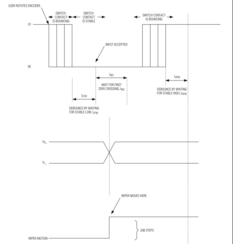
Click-and-Pop Suppression
The click-and-pop suppression feature reduces the
audible noise (clicks and pops) that results from wiper
transitions. The MAX5440 minimizes this noise by
allow-ing the wiper to change position only when V
H= V
L.
Each wiper has its own suppression and timeout
cir-cuitry. The MAX5440 changes wiper position when V
H= V
L, or after 32ms, whichever occurs first (see Figures
4a and 4b).
The suppression circuitry monitors left and right
chan-nels separately. In volume-control mode, when the first
wiper changes position, the second wiper has 32ms to
change or it will be forced to change.
MAX5440
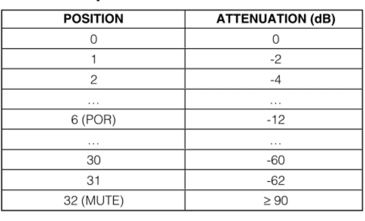
Table 1. Wiper Position and Attenuation
POSITION ATTENUATION (dB) 0 0 1 -2 2 -4 … … 6 (POR) -12 … … 30 -60 31 -62 32 (MUTE) ≥ 90 W0 W1 W0 W1 W0 W1 H_ L_ W0 W1 W0 W1 W0 W1 H_ L_ ROTATE CW ONCE ROTATE CW ONCE ROTATE CW ONCE ROTATE CW ONCE VOLUME LEVEL IS SET
VOLUME LEVEL IS SET BY W0
VOLUME LEVEL MAINTAINED BALANCE SHIFTS TO W1
VOLUME LEVEL MAINTAINED BALANCE SHIFTS TO W1
MAX5440
01
00 USER ROTATES ENCODER
tWS t HPW tLPW VH_ VL_ SWITCH CONTACT IS BOUNCING SWITCH CONTACT IS BOUNCING SWITCH CONTACT IS STABLE INPUT ACCEPTED
WAIT FOR FIRST ZERO CROSSING,tWS
DEBOUNCE BY WAITING FOR STABLE LOW,tLPW
DEBOUNCE BY WAITING FOR STABLE HIGH,tHPW
WIPER MOVES HERE
WIPER MOTION
2dB STEPS
MAX5440
tHPW
INPUT ACCEPTED
WAIT FOR FIRST ZERO CROSSING OR TIMEOUT,tWS 2dB STEPS tWS tLPW (tLPW +tWS) VH VL DEBOUNCE BY WAITING FOR STABLE LOW,tLPW
DEBOUNCE BY WAITING FOR STABLE HIGH,tHPW
01 00 SWITCH CONTACT IS BOUNCING SWITCH CONTACT IS STABLE SWITCH CONTACT IS BOUNCING
WIPER MOVES HERE
READY TO ACCEPT ANOTHER ENCODER INPUT SIGNAL
MAX5440
Power-On Reset
The power-on comparators monitor (V
DD- V
SS) and
(V
LOGIC- GND). A power-on reset is initiated when
either of the supplies is brought back to the normal
operating voltage. The power-on reset feature sets both
wipers to -12dB. The wipers initially wake up in mute
mode (-90dB) and move to the -12dB position when V
H= V
Lto eliminate clicks and pops during power-up.
With DC inputs at V
Hand V
L, the wipers move after
exceeding the timeout period. A power-on reset places
the MAX5440 in volume-control mode.
Shutdown (
SHDN
)
Upon entering shutdown, the MAX5440 stores the last
wiper settings. The wipers move to the L_ end of the
resistor string. The wipers move to the L_ end of the
resistor string when V
H= V
Lto eliminate clicks and pops
during shutdown. With DC inputs at V
Hand V
L, the
wipers move after exceeding the timeout period. Exiting
shutdown restores the wipers to their previous settings.
Mute Function (
MUTE
)
The MAX5440 features a mute function input,
MUTE
.
Successive low pulses on
MUTE
toggle its setting.
Activating the mute function forces both wipers to
maxi-mum attenuation (-90dB typ). Deactivating the mute
function returns the wipers to their previous settings.
Rotating the encoder clockwise (increasing gray code
count) also deactivates mute, setting the wipers to their
previous positions.
MUTE
is internally pulled high with a
45k
Ω
resistor to V
LOGIC. When both wipers are in the
tap 31 position (-62dB attenuation) further commands
to lower the volume (decreasing gray code count)
place the wipers in the mute position (see Table 1).
Rotating the encoder to a lower attenuation or a pulse
to
MUTE
returns the wipers to tap 31.
Mode Indicator (
MODEIND
)
The open-drain
MODEIND
indicates volume-control
mode or balance-control mode for the MAX5440.
Connect
MODEIND
to an LED with a series resistor to
V
LOGIC. When the LED is on, the MAX5440 is in
balance-control mode. When the LED is off, the MAX5440 is in
volume-control mode. See the
Mode Control (
MODE
)
section for more detail on switching between modes.
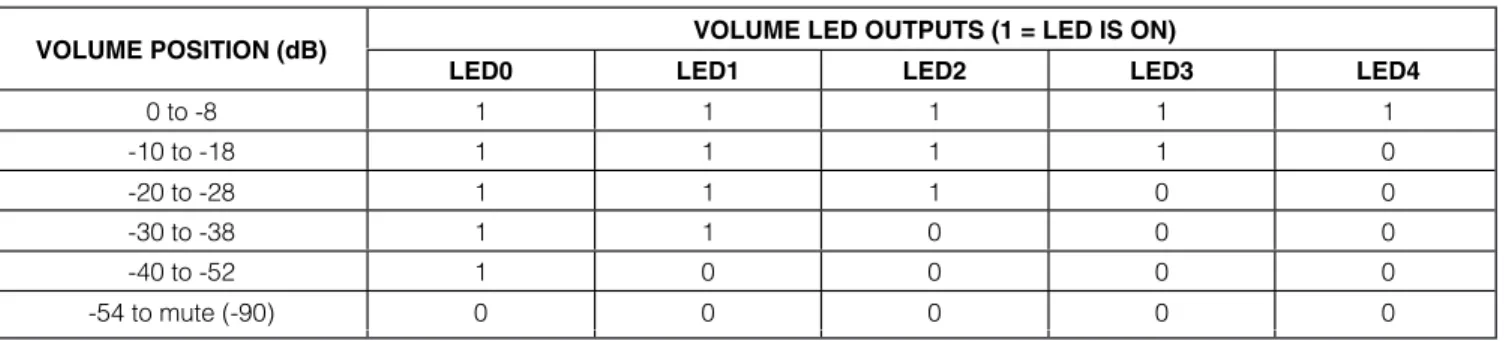
Level Indicator LEDs
The MAX5440 includes five indicator LED drivers to
dis-play the current wiper settings in either volume or
bal-ance mode. Connect the LEDIND_ outputs to the LEDs
and to V
LOGICthrough a series resistor as shown in the
typical application circuits.
In volume-control mode, all LEDs are off when the
wipers reach the highest attenuation levels (mute). All
LEDs are on at the lowest attenuation levels (0dB).
Table 2 shows the LED display as the wipers transition
through various attenuation levels.
In balance-control mode, only one LED is on at a time
to indicate the current balance setting. Figure 5 shows
the LEDs display for the current balance setting. When
LED2 is on, the display indicates that the channels are
centered or balanced at a set volume level. Turning the
encoder clockwise (an increasing gray code count)
turns LED3 on to represent a balance shift towards
channel 1. When LED4 turns on, the balance shifts
completely toward channel 1 and channel 0 is fully
attenuated. From a balanced position, turning the
encoder counterclockwise (a decreasing gray code
count) turns on LED1, and then LED0 to indicate a
bal-ance shift towards channel 0.
Table 2. LED Settings in Volume Mode
VOLUME LED OUTPUTS (1 = LED IS ON) VOLUME POSITION (dB)
LED0 LED1 LED2 LED3 LED4
0 to -8 1 1 1 1 1 -10 to -18 1 1 1 1 0 -20 to -28 1 1 1 0 0 -30 to -38 1 1 0 0 0 -40 to -52 1 0 0 0 0 -54 to mute (-90) 0 0 0 0 0
MAX5440
FULL L L + 12 L + 6 R + 6 R + 12 FULL R
CENTERED CW ROTATION (CH1) CCW ROTATION (CH0)
LED0 ON LED1 ON LED2 ON LED3 ON LED4 ON
Figure 5. LED Setting in Balance Mode
VDD VSS = -VDD VLOGIC VPEAK H1 L1 W1 SHDN LEFT INPUT RIGHT INPUT MODEIND HEADPHONE DRIVER L0 H0 W0 VLOGIC LEDIND4 LEDIND3 LEDIND0
GND MUTE MODE RENCODEA RENCODEA
LEDIND1 LEDIND2 ROTARY ENCODER MIDBIAS BIAS 0V MAX5440 (VDD + VSS) / 2
MAX5440
Multiple Button Pushes (
MODE
,
MUTE
)
The MAX5440 does not respond to simultaneous button
pushes. Pushing more than one button at the same
time stops the wipers in their present states. Only a
sin-gle button push configures the device.
Applications Information
Typical Application Circuit
The
Typical Operating Circuit
shows the MAX5440 in a
typical volume/balance application using a
single-sup-ply configuration. Figure 6 shows a typical
volume/bal-ance application circuit using the MAX5440 in a
dual-supply configuration. The MAX5440 does not
require external op amps because the bias is
generat-ed internally, and the wipers have internal low-power
buffers for low distortion. Connect the W_ outputs of the
MAX5440 to the left and right inputs of a stereo audio
amplifier, such as the MAX9761. The rotary encoder
controls the potentiometer attenuation levels without
using a microcontroller. Use the
MODE
input to switch
between volume-control and balance-control modes.
Chip Information
MAX5440
Functional Diagram
TIMING AND CONTROL
DEBOUNCE DEBOUNCE DEBOUNCE DEBOUNCE DEBOUNCE POSITION COUNTER POSITION COUNTER
UP/DOWN UP/DOWN MODEIND SHDN VLOGIC VDD VSS H0 W0 L0
GND RENCODEA RENCODEB MUTE
L1 W1 H1 MODE VLOGIC 0 1 2 3 4 28 30 31 29 0 1 2 3 4 28 29 30 31 MUTE MUTE BIAS GENERATOR MIDBIAS LEDIND0 LEDIND1 LEDIND2 LEDIND3 LEDIND4 45kΩ 45kΩ 45kΩ 45kΩ CLICK-AND-POP SUPPRESSION CIRCUITRY CLICK-AND-POP SUPPRESSION CIRCUITRY BIAS MAX5440
MAX5440
Maxim cannot assume responsibility for use of any circuitry other than circuitry entirely embodied in a Maxim product. No circuit patent licenses are implied. Maxim reserves the right to change the circuitry and specifications without notice at any time.
16 ____________________Maxim Integrated Products, 120 San Gabriel Drive, Sunnyvale, CA 94086 408-737-7600
PACKAGE OUTLINE, SSOP, 5.3 MM
1 1
21-0056 C
REV. DOCUMENT CONTROL NO.
APPROVAL
PROPRIETARY INFORMATION TITLE:
NOTES:
1. D&E DO NOT INCLUDE MOLD FLASH.
2. MOLD FLASH OR PROTRUSIONS NOT TO EXCEED .15 MM (.006"). 3. CONTROLLING DIMENSION: MILLIMETERS.
4. MEETS JEDEC MO150.
5. LEADS TO BE COPLANAR WITHIN 0.10 MM.
7.90 H L 0∞ 0.301 0.025 8∞ 0.311 0.037 0∞ 7.65 0.63 8∞ 0.95 MAX 5.38 MILLIMETERS B C D E e A1 DIM A SEE VARIATIONS 0.0256 BSC 0.010 0.004 0.205 0.002 0.015 0.008 0.212 0.008 INCHES MIN MAX 0.078 0.65 BSC 0.25 0.09 5.20 0.05 0.38 0.20 0.21 MIN 1.73 1.99 MILLIMETERS 6.07 6.07 10.07 8.07 7.07 INCHES D D D D D 0.239 0.239 0.397 0.317 0.278 MIN 0.249 0.249 0.407 0.328 0.289 MAX MIN 6.33 6.33 10.33 8.33 7.33 14L 16L 28L 24L 20L MAX N A D e A1 L C H E N 1 2 B 0.068