4-Mbit (256K x 16) Static RAM
Cypress Semiconductor Corporation • 198 Champion Court • San Jose
,
CA 95134-1709 • 408-943-2600Features
• Pin- and function-compatible with CY7C1041CV33 • High speed
— tAA =10 ns • Low active power
— ICC = 90 mA @ 10 ns (Industrial) • Low CMOS standby power
— ISB2 = 10 mA • 2.0 V data retention
• Automatic power-down when deselected • TTL-compatible inputs and outputs
• Easy memory expansion with CE and OE features • Available in lead-free 48-ball VFBGA, 44-lead (400-mil)
Molded SOJ and 44-pin TSOP II packages
Functional Description
[1]The CY7C1041DV33 is a high-performance CMOS Static RAM organized as 256K words by 16 bits. Writing to the device is accomplished by taking Chip Enable (CE) and Write Enable (WE) inputs LOW. If Byte LOW Enable (BLE) is LOW, then data from I/O pins (I/O0–I/O7), is written into the location specified on the address pins (A0–A17). If Byte HIGH Enable (BHE) is LOW, then data from I/O pins (I/O8–I/O15) is written into the location specified on the address pins (A0–A17). Reading from the device is accomplished by taking Chip Enable (CE) and Output Enable (OE) LOW while forcing the Write Enable (WE) HIGH. If Byte LOW Enable (BLE) is LOW, then data from the memory location specified by the address pins will appear on I/O0 – I/O7. If Byte HIGH Enable (BHE) is LOW, then data from memory will appear on I/O8 to I/O15. See the truth table at the back of this data sheet for a complete description of Read and Write modes.
The input/output pins (I/O0–I/O15) are placed in a high-impedance state when the device is deselected (CE HIGH), the outputs are disabled (OE HIGH), the BHE and BLE are disabled (BHE, BLE HIGH), or during a Write operation (CE LOW, and WE LOW).
The CY7C1041DV33 is available in a standard 44-pin 400-mil-wide body width SOJ and 44-pin TSOP II package with center power and ground (revolutionary) pinout, as well as a 48-ball fine-pitch ball grid array (FBGA) package.
Note
1. For guidelines on SRAM system design, please refer to the “System Design Guidelines” Cypress application note, available on the internet at www.cypress.com. 14 15
Logic Block Diagram
A1 A2 A3 A4 A5 A6 A7 A8 COLUMN DECODER RO W DE CO DE R SE NS E AM PS INPUT BUFFER 256K × 16 A0 A11 A12 A13 A A A16 A17 A9 A10 I/O0–I/O7 OE I/O8–I/O15 CE WE BLE BHE
Selection Guide
–10 (Industrial) –12 (Automotive)[2] Unit
Maximum Access Time 10 12 ns
Maximum Operating Current 90 95 mA
Maximum CMOS Standby Current 10 15 mA
Pin Configurations
Note
2. Automotive product information is Preliminary.
48-ball Mini FBGA
WE VCC A11 A10 NC A6 A0 A3 CE I/O2 I/O0 I/O1 A4 A5 I/O3 I/O5 I/O4 I/O6 I/O7 VSS A9 A8 OE VSS A7 I/O8 BHE NC A17 A2 A1 BLE VCC I/O9 I/O10 I/O11 I/O12 I/O13 I/O14 I/O15 A15 A14 A13 A12 NC NC NC 3 2 4 5 6 1 D E B A C F G H A16 Top View SOJ TSOP II WE 1 2 3 4 5 6 7 8 9 10 11 14 31 32 36 35 34 33 37 40 39 38 12 13 41 44 43 42 16 15 29 30 VCC A5 A6 A7 A8 A0 A1 OE VSS A17 I/O15 A2 CE I/O2 I/O0 I/O1 BHE A3 A4 18 17 20 19 I/O3 27 28 25 26 22 21 23 24 VSS I/O6 I/O4 I/O5 I/O7 A16 A15 BLE VCC I/O14 I/O13 I/O12 I/O11 I/O10 I/O9 I/O8 A14 A13 A12 A11 A9 A10 NC (Top View)
Maximum Ratings
(Above which the useful life may be impaired. For user guide-lines, not tested.)
Storage Temperature ... –65°C to +150°C Ambient Temperature with
Power Applied... –55°C to +125°C Supply Voltage on VCC to Relative GND[3].... –0.3V to +4.6V DC Voltage Applied to Outputs
in High-Z State[3]...–0.3V to VCC +0.3V DC Input Voltage[3]...–0.3V to VCC +0.3V
Current into Outputs (LOW)... 20 mA Static Discharge Voltage... ...>2001V (per MIL-STD-883, Method 3015)
Latch-up Current... >200 mA
Operating Range
Range Ambient Temperature VCC Speed Industrial –40°C to +85°C 3.3V ± 0.3V 10 ns Automotive –40°C to +125°C 3.3V ± 0.3V 12 ns Note3. Minimum voltage is–2.0V and VIH(max) = VCC + 2V for pulse durations of less than 20 ns.
DC Electrical Characteristics
Over the Operating RangeParameter Description Test Conditions –10 (Industrial) –12 (Automotive) Unit
Min. Max. Min. Max.
VOH Output HIGH Voltage VCC = Min., IOH = –4.0 mA 2.4 2.4 V
VOL Output LOW Voltage VCC = Min., IOL = 8.0 mA 0.4 0.4 V
VIH[3] Input HIGH
Voltage
2.0 VCC + 0.3 2.0 VCC + 0.3 V
VIL[3] Input LOW Voltage –0.3 0.8 –0.3 0.8 V
IIX Input Leakage Current GND < VI < VCC –1 +1 –1 +1 µA
IOZ Output Leakage
Current
GND < VOUT < VCC, Output Disabled –1 +1 –1 +1 µA
ICC VCC Operating Supply Current VCC = Max., f = fMAX = 1/tRC 100MHz 90 - mA 83MHz 80 95 mA 66MHz 70 85 mA 40MHz 60 75 mA ISB1 Automatic CE Power-down Current—TTL Inputs Max. VCC, CE > VIH VIN > VIH or VIN < VIL, f = fMAX 20 25 mA ISB2 Automatic CE Power-down Current—CMOS Inputs Max. VCC, CE > VCC – 0.3V, VIN > VCC – 0.3V, or VIN < 0.3V, f = 0 10 15 mA
Capacitance
[4]Parameter Description Test Conditions Max. Unit
CIN Input Capacitance TA = 25°C, f = 1 MHz, VCC = 3.3V 8 pF
COUT I/O Capacitance 8 pF
Thermal Resistance
[4]Parameter Description Test Conditions PackageFBGA PackageSOJ PackageTSOP II Unit
ΘJA Thermal Resistance
(Junction to Ambient)
Still Air, soldered on a 3 × 4.5 inch, four-layer printed circuit
board
27.89 57.91 50.66 °C/W
ΘJC Thermal Resistance
(Junction to Case)
14.74 36.73 17.17 °C/W
AC Test Loads and Waveforms
[5]90% 10% 3.0V GND 90% 10%
ALL INPUT PULSES
* CAPACITIVE LOAD CONSISTS OF ALL COMPONENTS OF THE TEST ENVIRONMENT
Rise Time: 1 V/ns Fall Time: 1 V/ns
30 pF* OUTPUT Z = 50Ω 50Ω 1.5V (b) (a) 3.3V OUTPUT 5 pF (c) R 317Ω R2 351Ω High-Z Characteristics 10 ns device Notes
4. Tested initially and after any design or process changes that may affect these parameters.
5. AC characteristics (except High-Z) are tested using the load conditions shown in Figure (a). High-Z characteristics are tested for all speeds using the test load shown in Figure (c).
AC Switching Characteristics
Over the Operating Range[6]Parameter Description –10 (Industrial) –12 (Automotive) Unit
Min. Max. Min. Max.
Read Cycle
tpower[7] VCC(typical) to the first access 100 100 µs
tRC Read Cycle Time 10 12 ns
tAA Address to Data Valid 10 12 ns
tOHA Data Hold from Address Change 3 3 ns
tACE CE LOW to Data Valid 10 12 ns
tDOE OE LOW to Data Valid 5 6 ns
tLZOE OE LOW to Low-Z 0 0 ns
tHZOE OE HIGH to High-Z[8, 9] 5 6 ns
tLZCE CE LOW to Low-Z[9] 3 3 ns
tHZCE CE HIGH to High-Z[8, 9] 5 6 ns
tPU CE LOW to Power-Up 0 0 ns
tPD CE HIGH to Power-Down 10 12 ns
tDBE Byte Enable to Data Valid 5 6 ns
tLZBE Byte Enable to Low-Z 0 0 ns
tHZBE Byte Disable to High-Z 6 6 ns
Notes
6. Test conditions assume signal transition time of 3 ns or less, timing reference levels of 1.5V, input pulse levels of 0 to 3.0V, and output loading of the specified IOL/IOH and 30-pF load capacitance.
7. tPOWER gives the minimum amount of time that the power supply should be at typical VCC values until the first memory access can be performed.
8. tHZOE, tHZCE,tHZBE and tHZWE are specified with a load capacitance of 5 pF as in part (c) of AC Test Loads. Transition is measured when the outputs enter a high
impedance state.
9. At any given temperature and voltage condition, tHZCE is less than tLZCE, tHZOE is less than tLZOE, tHZBE is less than tLZBE, and tHZWE is less than tLZWE for any given device.
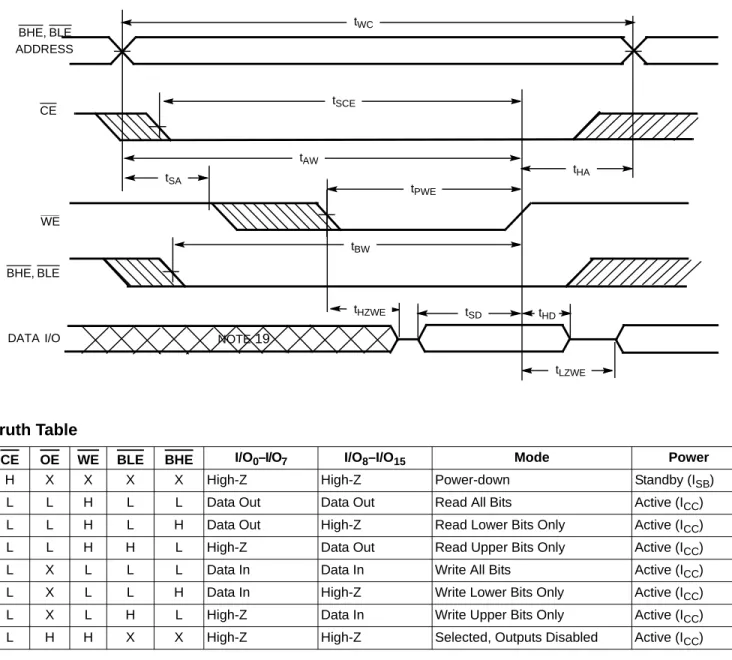
Write Cycle[10, 11]
tWC Write Cycle Time 10 12 ns
tSCE CE LOW to Write End 7 8 ns
tAW Address Set-Up to Write End 7 8 ns
tHA Address Hold from Write End 0 0 ns
tSA Address Set-Up to Write Start 0 0 ns
tPWE WE Pulse Width 7 8 ns
tSD Data Set-Up to Write End 5 6 ns
tHD Data Hold from Write End 0 0 ns
tLZWE WE HIGH to Low-Z[9] 3 3 ns
tHZWE WE LOW to High-Z[8, 9] 5 6 ns
tBW Byte Enable to End of Write 7 8 ns
Data Retention Characteristics
Over the Operating RangeParameter Description Conditions[12] Min. Max. Unit
VDR VCC for Data Retention 2.0 V
ICCDR Data Retention Current VCC = VDR = 2.0V,
CE > VCC – 0.3V,
VIN > VCC – 0.3V or VIN < 0.3V
Ind’l 10 mA
Auto 15
mA
tCDR[4] Chip Deselect to Data Retention Time 0 ns
tR[13] Operation Recovery Time tRC ns
Data Retention Waveform
AC Switching Characteristics
Over the Operating Range[6](continued)Parameter Description –10 (Industrial) –12 (Automotive) Unit
Min. Max. Min. Max.
3.0V 3.0V
tCDR
VDR> 2V
DATA RETENTION MODE
tR
CE
VCC
Notes
10. The internal Write time of the memory is defined by the overlap of CE LOW, and WE LOW. CE and WE must be LOW to initiate a Write, and the transition of either of these signals can terminate the Write. The input data set-up and hold timing should be referenced to the leading edge of the signal that terminates the Write.
11. The minimum Write cycle time for Write Cycle No. 4 (WE controlled, OE LOW) is the sum of tHZWE and tSD. 12. No input may exceed VCC + 0.3V.
Switching Waveforms
Read Cycle No. 1[14, 15]
Read Cycle No. 2 (OE Controlled)[15, 16]
PREVIOUS DATA VALID DATA VALID
tRC tAA tOHA ADDRESS DATA OUT 50% 50% DATA VALID tRC tACE tDOE tLZOE tLZCE tPU HIGH IMPEDANCE tHZOE tHZBE tPD HIGH OE CE ICC ISB IMPEDANCE ADDRESS DATA OUT VCC SUPPLY tDBE tLZBE tHZCE BHE, BLE CURRENT ICC ISB Notes
14. Device is continuously selected. OE, CE, BHE and/or BHE = VIL. 15. WE is HIGH for Read cycle.
Write Cycle No. 1 (CE Controlled)[17, 18]
Switching Waveforms
(continued)tHD tSD tSCE tSA tHA tAW tPWE tWC BW DATAI/O ADDRESS CE WE BHE, BLE t Notes
17. Data I/O is high-impedance if OE or BHE and/or BLE = VIH.
Write Cycle No. 2 (BLE or BHE Controlled)
Write Cycle No. 3 (WE Controlled, OE HIGH During Write)[17, 18]
Switching Waveforms
(continued)tHD tSD tBW tSA tHA tAW tPWE tWC tSCE DATAI/O ADDRESS BHE, BLE WE CE tHD t SD tPWE tSA tHA tAW tSCE tWC t HZOE DATAINVALID CE ADDRESS WE DATA I/O OE NOTE19 BHE, BLE Note
Write Cycle No. 4(WE Controlled, OE LOW)
Truth Table
CE OE WE BLE BHE I/O0–I/O7 I/O8–I/O15 Mode Power
H X X X X High-Z High-Z Power-down Standby (ISB)
L L H L L Data Out Data Out Read All Bits Active (ICC)
L L H L H Data Out High-Z Read Lower Bits Only Active (ICC)
L L H H L High-Z Data Out Read Upper Bits Only Active (ICC)
L X L L L Data In Data In Write All Bits Active (ICC)
L X L L H Data In High-Z Write Lower Bits Only Active (ICC)
L X L H L High-Z Data In Write Upper Bits Only Active (ICC)
L H H X X High-Z High-Z Selected, Outputs Disabled Active (ICC)
Switching Waveforms
(continued)tHD tSD tSCE tHA tAW tPWE tWC tBW DATA I/O ADDRESS CE WE BHE, BLE tSA tLZWE tHZWE NOTE 19 BHE, BLE
Ordering Information
Speed (ns) Ordering Code PackageDiagram Package Type
Operating Range
10 CY7C1041DV33-10BVI 51-85150 48-ball VFBGA Industrial
CY7C1041DV33-10BVXI 48-ball VFBGA (Pb-Free)
CY7C1041DV33-10VXI 51-85082 44-lead (400-mil) Molded SOJ (Pb-Free)
12 CY7C1041DV33-12BVXE 51-85150 48-ball VFBGA (Pb-Free) Automotive
CY7C1041DV33-12VXE 51-85082 44-lead (400-mil) Molded SOJ (Pb-Free)
CY7C1041DV33-12ZSXE 51-85087 44-pin TSOP II (Pb-Free)
Please contact your local Cypress sales representative for availability of these parts
Ordering Information
Speed
(ns) Ordering Code
Package
Diagram Package Type
Operating Range
Package Diagrams
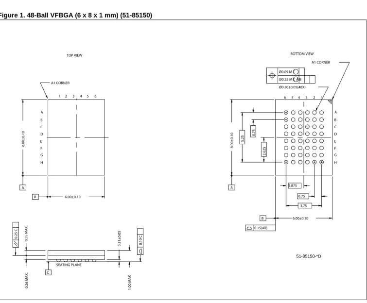
Figure 1. 48-Ball VFBGA (6 x 8 x 1 mm) (51-85150)
A 1 A1 CORNER 0.75 0.75 Ø0.30±0.05(48X) Ø0.25 M C A B Ø0.05 M C B A 0.15(4X) 0.21±0.05 1.00 MAX C SEATING PLANE 0.55 MAX. 0.25 C 0.10 C A1 CORNER
TOP VIEW BOTTOM VIEW
2 3 4 3.75 5.25 B C D E F G H 6 5 4 5 6 2 3 1 D H F G E C B A 6.00±0.10 8.00±0.10 A 8.00±0.10 6.00±0.10 B 1.875 2.625 0.26 MAX. 51-85150-*D
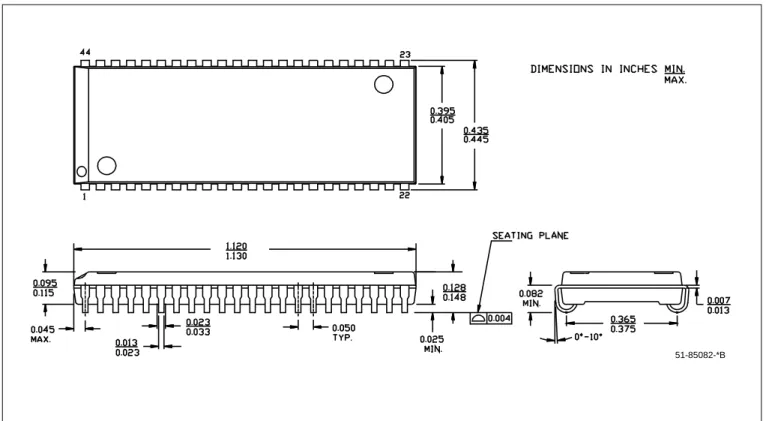
Figure 2. 44-lead (400-mil) Molded SOJ (51-85082)
Package Diagrams
(continued)Document #: 38-05473 Rev. *D Page 13 of 14 © Cypress Semiconductor Corporation, 2006. The information contained herein is subject to change without notice. Cypress Semiconductor Corporation assumes no responsibility for the use of any circuitry other than circuitry embodied in a Cypress product. Nor does it convey or imply any license under patent or other rights. Cypress products are not warranted nor intended to be used for medical, life support, life saving, critical control or safety applications, unless pursuant to an express written agreement with Cypress. Furthermore, Cypress does not authorize its All products and company names mentioned in this document may be the trademarks of their respective holders.
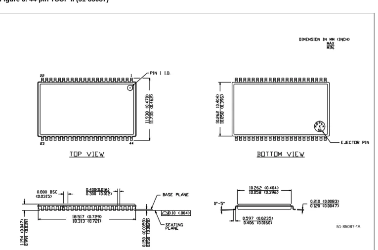
Figure 3. 44-pin TSOP II (51-85087)
Package Diagrams
(continued)Document History Page
Document Title: CY7C1041DV33 4-Mbit (256K x 16) Static RAM Document Number: 38-05473
REV. ECN NO. Issue Date Orig. of
Change Description of Change
** 201560 See ECN SWI Advance Data sheet for C9 IPP
*A 233729 See ECN RKF 1.AC, DC parameters are modified as per EROS(Spec # 01-2165)
2.Pb-free offering in the ‘Ordering information’
*B 351117 See ECN PCI Changed from Advance to Preliminary
Removed 15 and 20 ns Speed bin
Corrected DC voltage (min) value in maximum ratings section from - 0.5 to - 0.3V
Redefined ICC values for Com’l and Ind’l temperature ranges
ICC (Com’l):Changed from 100, 80 and 67 mA to 90, 80 and 75 mA for 8, 10 and 12ns speed bins respectively
ICC (Ind’l): Changed from 80 and 67 mA to 90 and 85 mA for 10 and 12ns speed bins respectively
Added Static Discharge Voltage and latch-up current spec Added VIH(max)spec in Note# 2
Changed Note# 4 on AC Test Loads
Changed reference voltage level for measurement of Hi-Z parameters from ±500 mV to ±200 mV
Added Data Retention Characteristics/Waveform and footnote # 11, 12 Added Write Cycle (WE Controlled, OE HIGH During Write) Timing Diagram Changed Package Diagram name from 44-pin TSOP II Z44 to 44-pin TSOP II ZS44 and from 44-lead (400-mil) Molded SOJ V34 to 44-lead (400-mil) Molded SOJ V44
Changed part names from Z to ZS in the Ordering Information Table Added 8 ns Product Information
Added Lead-Free Ordering Information Shaded Ordering Information Table
*C 446328 See ECN NXR Converted from Preliminary to Final
Removed -8 speed bin
Removed Commercial Operating Range product information Included Automotive Operating Range product information Updated Thermal Resistance table
Updated footnote #8 on High-Z parameter measurement
Updated the ordering information and replaced Package Name column with Package Diagram in the Ordering Information Table