M
MCP2551
Features
• Supports 1 Mb/s operation
• Implements ISO-11898 standard physical layer requirements
• Suitable for 12V and 24V systems
• Externally-controlled slope for reduced RFI emissions
• Detection of ground fault (permanent dominant) on TXD input
• Power-on reset and voltage brown-out protection • An unpowered node or brown-out event will not
disturb the CAN bus
• Low current standby operation
• Protection against damage due to short-circuit conditions (positive or negative battery voltage) • Protection against high-voltage transients • Automatic thermal shutdown protection • Up to 112 nodes can be connected
• High noise immunity due to differential bus implementation
• Temperature ranges:
- Industrial (I): -40°C to +85°C - Extended (E): -40°C to +125°C
Package Types
Block Diagram
RS
CANH CANL VREF
TXD VSS
VDD
RXD 1 2 3 4
8 7 6 5 PDIP/SOIC
M
C
P
2551
Thermal Shutdown
VDD
TXD
VDD
TXD Dominant
Detect
Driver Control
MCP2551
MCP2551
1.0
DEVICE OVERVIEW
The MCP2551 is a high-speed CAN, fault-tolerant device that serves as the interface between a CAN protocol controller and the physical bus. The MCP2551 provides differential transmit and receive capability for the CAN protocol controller and is fully compatible with the ISO-11898 standard, including 24V requirements. It will operate at speeds of up to 1 Mb/s.
Typically, each node in a CAN system must have a device to convert the digital signals generated by a CAN controller to signals suitable for transmission over the bus cabling (differential output). It also provides a buffer between the CAN controller and the high-voltage spikes that can be generated on the CAN bus by outside sources (EMI, ESD, electrical transients, etc.).
1.1
Transmitter Function
The CAN bus has two states: Dominant and Recessive. A dominant state occurs when the differential voltage between CANH and CANL is greater than a defined voltage (e.g.,1.2V). A recessive state occurs when the differential voltage is less than a defined voltage (typically 0V). The dominant and recessive states correspond to the low and high state of the TXD input pin, respectively. However, a dominant state initiated by another CAN node will override a recessive state on the CAN bus.
1.1.1 MAXIMUM NUMBER OF NODES The MCP2551 CAN outputs will drive a minimum load of 45Ω
,
allowing a maximum of 112 nodes to be connected (given a minimum differential input resistance of 20 kΩ and a nominal termination resistor value of 120Ω).1.2
Receiver Function
The RXD output pin reflects the differential bus voltage between CANH and CANL. The low and high states of the RXD output pin correspond to the dominant and recessive states of the CAN bus, respectively.
1.3
Internal Protection
CANH and CANL are protected against battery short-circuits and electrical transients that can occur on the
1.4
Operating Modes
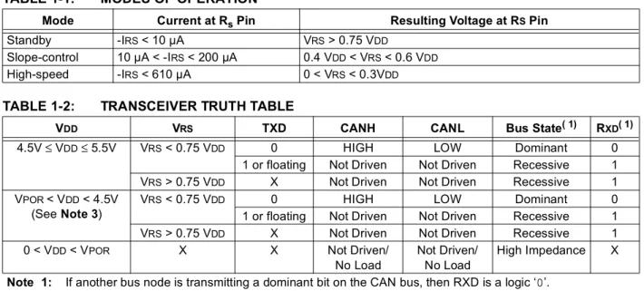
The RS pin allows three modes of operation to be
selected: • High-Speed • Slope-Control • Standby
These modes are summarized in Table 1-1.
When in High-speed or Slope-control mode, the drivers for the CANH and CANL signals are internally regu-lated to provide controlled symmetry in order to mini-mize EMI emissions.
Additionally, the slope of the signal transitions on CANH and CANL can be controlled with a resistor connected from pin 8 (RS) to ground, with the slope
proportional to the current output at RS, further reducing EMI emissions.
1.4.1 HIGH-SPEED
High-speed mode is selected by connecting the RS pin to VSS. In this mode, the transmitter output drivers have fast output rise and fall times to support high-speed CAN bus rates.
1.4.2 SLOPE-CONTROL
Slope-control mode further reduces EMI by limiting the rise and fall times of CANH and CANL. The slope, or slew rate (SR), is controlled by connecting an external resistor (REXT) between RS and VOL (usually ground).
The slope is proportional to the current output at the RS
pin. Since the current is primarily determined by the slope-control resistance value REXT, a certain slew rate is achieved by applying a respective resistance. Figure 1-1 illustrates typical slew rate values as a function of the slope-control resistance value. 1.4.3 STANDBY MODE
The device may be placed in standby or “SLEEP” mode by applying a high-level to RS. In SLEEP mode, the transmitter is switched off and the receiver operates at a lower current. The receive pin on the controller side (RXD) is still functional but will operate at a slower rate. The attached microcontroller can monitor RXD for CAN bus activity and place the transceiver into normal operation via the RS pin (at higher bus rates, the first CAN message may be lost).
MCP2551
TABLE 1-1: MODES OF OPERATION
TABLE 1-2: TRANSCEIVER TRUTH TABLE
FIGURE 1-1: SLEW RATE VS. SLOPE-CONTROL RESISTANCE VALUE
Mode Current at Rs Pin Resulting Voltage at RS Pin
Standby -IRS < 10 µA VRS > 0.75 VDD
Slope-control 10 µA < -IRS < 200 µA 0.4 VDD < VRS < 0.6 VDD
High-speed -IRS < 610 µA 0 < VRS < 0.3VDD
VDD VRS TXD CANH CANL Bus State( 1) RXD( 1)
4.5V ≤ VDD≤ 5.5V VRS < 0.75 VDD 0 HIGH LOW Dominant 0 1 or floating Not Driven Not Driven Recessive 1 VRS > 0.75 VDD X Not Driven Not Driven Recessive 1
VPOR < VDD < 4.5V
(See Note 3)
VRS < 0.75 VDD 0 HIGH LOW Dominant 0
1 or floating Not Driven Not Driven Recessive 1 VRS > 0.75 VDD X Not Driven Not Driven Recessive 1 0 < VDD < VPOR X X Not Driven/
No Load
Not Driven/ No Load
High Impedance X
Note 1: If another bus node is transmitting a dominant bit on the CAN bus, then RXD is a logic ‘0’. 2: X = “don’t care”.
3: Device drivers will function, although outputs are not ensured to meet the ISO-11898 specification.
0 5 10 15 20 25
10 20 30 40 49 60 70 76 90 100 110 120 Resistance (kΩ)
MCP2551
1.5
TXD Permanent Dominant
Detection
If the MCP2551 detects an extended low state on the TXD input, it will disable the CANH and CANL output drivers in order to prevent the corruption of data on the CAN bus. The drivers are disabled if TXD is low for more than 1.25 ms (minimum). This implies a maximum bit time of 62.5 µs (16 kb/s bus rate), allowing up to 20 consecutive transmitted dominant bits during a multiple bit error and error frame scenario. The drivers remain disabled as long as TXD remains low. A rising edge on TXD will reset the timer logic and enable the CANH and CANL output drivers.
1.6
Power-on Reset
When the device is powered on, CANH and CANL remain in a high-impedance state until VDD reaches the
voltage-level VPORH. In addition, CANH and CANL will remain in a high-impedance state if TXD is low when VDD reaches VPORH. CANH and CANL will become active only after TXD is asserted high. Once powered on, CANH and CANL will enter a high-impedance state if the voltage level at VDD falls below VPORL, providing
voltage brown-out protection during normal operation.
1.7
Pin Descriptions
The 8-pin pinout is listed in Table 1-3. TABLE 1-3: MCP2551 PINOUT
1.7.1 TRANSMITTER DATA INPUT (TXD) TXD is a TTL-compatible input pin. The data on this pin is driven out on the CANH and CANL differential output pins. It is usually connected to the transmitter data output of the CAN controller device. When TXD is low, CANH and CANL are in the dominant state. When TXD is high, CANH and CANL are in the recessive state, provided that another CAN node is not driving the CAN bus with a dominant state. TXD has an internal pull-up resistor (nominal 25 kΩ to VDD).
1.7.2 GROUND SUPPLY (VSS)
Ground supply pin.
1.7.3 SUPPLY VOLTAGE (VDD)
Positive supply voltage pin.
1.7.4 RECEIVER DATA OUTPUT (RXD) RXD is a CMOS-compatible output that drives high or low depending on the differential signals on the CANH and CANL pins and is usually connected to the receiver data input of the CAN controller device. RXD is high when the CAN bus is recessive and low in the dominant state.
1.7.5 REFERENCE VOLTAGE (VREF)
Reference Voltage Output (Defined as VDD/2).
1.7.6 CAN LOW (CANL)
The CANL output drives the low side of the CAN differential bus. This pin is also tied internally to the receive input comparator.
1.7.7 CAN HIGH (CANH)
The CANH output drives the high-side of the CAN differential bus. This pin is also tied internally to the receive input comparator.
1.7.8 SLOPE RESISTOR INPUT (RS)
The RS pin is used to select High-speed, Slope-control or Standby modes via an external biasing resistor.
Pin Number
Pin
Name Pin Function
1 TXD Transmit Data Input 2 VSS Ground
3 VDD Supply Voltage
4 RXD Receive Data Output 5 VREF Reference Output Voltage 6 CANL CAN Low-Level Voltage I/O 7 CANH CAN High-Level Voltage I/O 8 RS Slope-Control Input
MCP2551
MCP2551
2.0
ELECTRICAL
CHARACTERISTICS
2.1
Terms and Definitions
A number of terms are defined in ISO-11898 that are used to describe the electrical characteristics of a CAN transceiver device. These terms and definitions are summarized in this section.
2.1.1 BUS VOLTAGE
VCANL and VCANH denote the voltages of the bus line wires CANL and CANH relative to ground of each individual CAN node.
2.1.2 COMMON MODE BUS VOLTAGE RANGE
Boundary voltage levels of VCANL and VCANH with respect to ground, for which proper operation will occur, if up to the maximum number of CAN nodes are connected to the bus.
2.1.3 DIFFERENTIAL INTERNAL CAPACITANCE, CDIFF (OF A CAN
NODE)
Capacitance seen between CANL and CANH during the recessive state when the CAN node is disconnected from the bus (see Figure 2-1).
2.1.4 DIFFERENTIAL INTERNAL RESISTANCE, RDIFF (OF A CAN
NODE)
Resistance seen between CANL and CANH during the recessive state when the CAN node is disconnected from the bus (see Figure 2-1).
2.1.5 DIFFERENTIAL VOLTAGE, VDIFF
(OF CAN BUS)
Differential voltage of the two-wire CAN bus, value VDIFF = VCANH - VCANL.
2.1.6 INTERNAL CAPACITANCE, CIN (OF
A CAN NODE)
Capacitance seen between CANL (or CANH) and ground during the recessive state when the CAN node is disconnected from the bus (see Figure 2-1). 2.1.7 INTERNAL RESISTANCE, RIN (OF A
CAN NODE)
Resistance seen between CANL (or CANH) and ground during the recessive state when the CAN node is disconnected from the bus (see Figure 2-1). FIGURE 2-1: PHYSICAL LAYER
DEFINITIONS
RIN
RIN RDIFF
CIN CIN
CDIFF
CANL
CANH GROUND ECU
MCP2551
Absolute Maximum Ratings†
VDD...7.0V
DC Voltage at TXD, RXD, VREF and VS... -0.3V to VDD + 0.3V DC Voltage at CANH, CANL (Note 1) ... -42V to +42V Transient Voltage on Pins 6 and 7 (Note 2) ...-250V to +250V Storage temperature ...-55°C to +150°C Operating ambient temperature ...-40°C to +125°C Virtual Junction Temperature, TVJ (Note 3)...-40°C to +150°C
Soldering temperature of leads (10 seconds) ...+300°C ESD protection on CANH and CANL pins (Note 4) ...6 kV ESD protection on all other pins (Note 4) ...4 kV
Note 1: Short-circuit applied when TXD is high and low.
2: In accordance with ISO-7637.
3: In accordance with IEC 60747-1.
4: Classification A: Human Body Model.
† NOTICE: Stresses above those listed under “Maximum ratings” may cause permanent damage to the device. This is a stress rating only and functional operation of the device at those or any other conditions above those indicated in the operational listings of this specification is not implied. Exposure to maximum rating conditions for extended periods may affect device reliability.
MCP2551
2.2
DC Characteristics
DC SpecificationsElectrical Characteristics:
Industrial (I): TAMB = -40°C to +85°C VDD = 4.5V to 5.5V Extended (E):TAMB = -40°C to +125°C VDD = 4.5V to 5.5V
Param
No. Sym Characteristic Min Max Units Conditions Supply
D1 IDD Supply Current — 75 mA Dominant; VTXD = 0.8V; VDD
D2 — 10 mA Recessive; VTXD = +2V;
RS = 47 kΩ
D3 — 365 µA -40°C ≤ TAMB≤ +85°C,
Standby; (Note 2)
— 465 µA -40°C ≤ TAMB≤ +125°C, Standby; (Note 2)
D4 VPORH High-level of the power-on reset comparator
3.8 4.3 V CANH, CANL outputs are
active when VDD > VPORH D5 VPORL Low-level of the power-on reset
comparator
3.4 4.0 V CANH, CANL outputs are not
active when VDD < VPORL D6 VPORD Hysteresis of power-on reset
comparator
0.3 0.8 V Note 1
Bus Line (CANH; CANL) Transmitter
D7 VCANH(r);VCANL(r) CANH, CANL Recessive bus voltage
2.0 3.0 V VTXD = VDD; no load.
D8 IO(CANH)(reces) IO(CANL)(reces)
Recessive output current -2 +2 mA -2V < V(CAHL,CANH) < +7V, 0V <VDD < 5.5V
D9 -10 +10 mA -5V < V(CANL,CANH) < +40V,
0V <VDD < 5.5V D10 VO(CANH) CANH dominant output voltage 2.75 4.5 V VTXD = 0.8V D11 VO(CANL) CANL dominant output voltage 0.5 2.25 V VTXD = 0.8V D12 VDIFF(r)(o) Recessive differential output
voltage
-500 +50 mV VTXD = 2V; no load
D13 VDIFF(d)(o) Dominant differential output voltage
1.5 3.0 V VTXD = 0.8V; VDD = 5V 40Ω < RL < 60Ω(Note 2)
D14 IO(SC)(CANH) CANH short-circuit output current — -200 mA VCANH = -5V
D15 — -100
(typical)
mA VCANH = -40V, +40V. (Note 1)
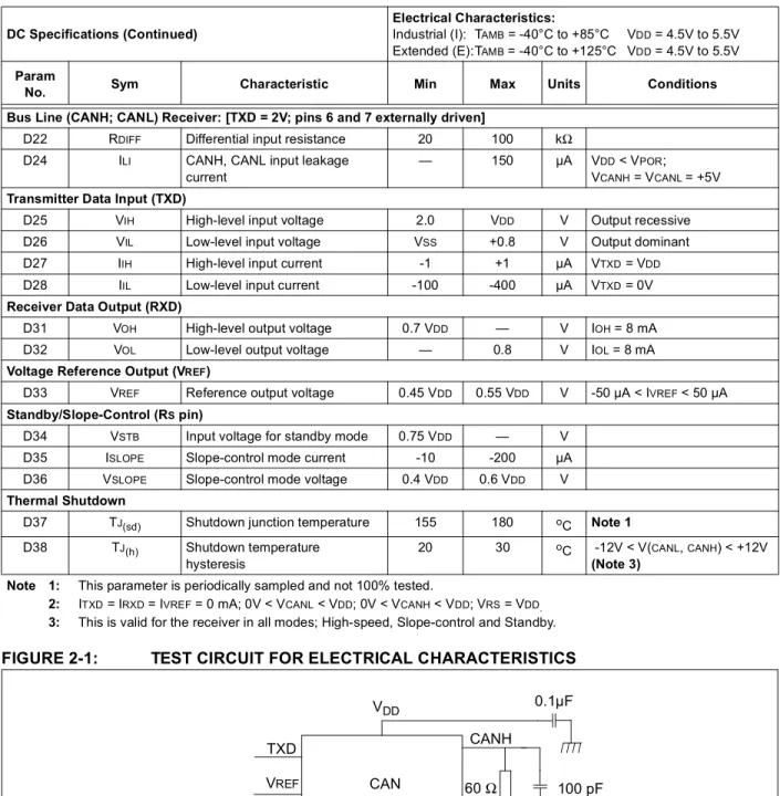
D16 IO(SC)(CANL)l CANL short-circuit output current — 200 mA VCANL = -40V, +40V. (Note 1) Bus Line (CANH; CANL) Receiver: [TXD = 2V; pins 6 and 7 externally driven]
D17 VDIFF(r)(i) Recessive differential input voltage
-1.0 +0.5 V -2V < V(CANL, CANH) < +7V
(Note 3)
-1.0 +0.4 V -12V < V(CANL, CANH) < +12V
(Note 3)
D18 VDIFF(d)(i) Dominant differential input voltage
0.9 5.0 V -2V < V(CANL, CANH) < +7V
MCP2551
FIGURE 2-1: TEST CIRCUIT FOR ELECTRICAL CHARACTERISTICS Bus Line (CANH; CANL) Receiver: [TXD = 2V; pins 6 and 7 externally driven]
D22 RDIFF Differential input resistance 20 100 kΩ
D24 ILI CANH, CANL input leakage
current
— 150 µA VDD < VPOR; VCANH = VCANL = +5V
Transmitter Data Input (TXD)
D25 VIH High-level input voltage 2.0 VDD V Output recessive
D26 VIL Low-level input voltage VSS +0.8 V Output dominant
D27 IIH High-level input current -1 +1 µA VTXD = VDD
D28 IIL Low-level input current -100 -400 µA VTXD = 0V
Receiver Data Output (RXD)
D31 VOH High-level output voltage 0.7 VDD — V IOH = 8 mA
D32 VOL Low-level output voltage — 0.8 V IOL = 8 mA
Voltage Reference Output (VREF)
D33 VREF Reference output voltage 0.45 VDD 0.55 VDD V -50 µA < IVREF < 50 µA
Standby/Slope-Control (RS pin)
D34 VSTB Input voltage for standby mode 0.75 VDD — V
D35 ISLOPE Slope-control mode current -10 -200 µA
D36 VSLOPE Slope-control mode voltage 0.4 VDD 0.6 VDD V
Thermal Shutdown
D37 TJ(sd) Shutdown junction temperature 155 180 oC Note 1 D38 TJ(h) Shutdown temperature
hysteresis
20 30 oC -12V < V(CANL, CANH) < +12V
(Note 3)
2.2
DC Characteristics (Continued)
DC Specifications (Continued)
Electrical Characteristics:
Industrial (I): TAMB = -40°C to +85°C VDD = 4.5V to 5.5V Extended (E):TAMB = -40°C to +125°C VDD = 4.5V to 5.5V
Param
No. Sym Characteristic Min Max Units Conditions
Note 1: This parameter is periodically sampled and not 100% tested.
2: ITXD = IRXD = IVREF = 0 mA; 0V < VCANL < VDD; 0V < VCANH < VDD; VRS = VDD.
3: This is valid for the receiver in all modes; High-speed, Slope-control and Standby.
RS
Rext GND
RXD VREF
TXD
60Ω 100 pF
30 pF
CANH
CANL CAN
Transceiver
Note: RS may be connected to VDD or GND via a load resistor depending on desired operating mode as described in Section 1.7.8, “Slope Resistor Input (Rs)”.
0.1µF VDD
MCP2551
FIGURE 2-2: TEST CIRCUIT FOR AUTOMOTIVE TRANSIENTS
FIGURE 2-3: HYSTERESIS OF THE RECEIVER RS
Rext GND
RXD VREF
TXD
60Ω 500 pF
500 pF
Note: RS may be connected to VDD or GND via a load resistor depending on desired operating mode as described in Section 1.7.8, “Slope Resistor Input (Rs)”
CANH
CANL CAN
Transceiver
Schaffner Generator
The wave forms of the applied transients shall be in accordance with “ISO-7637, Part 1”,test pulses 1, 2, 3a and 3b.
VOH
VOL
0.5 0.9
hysteresis D19
Vdiff (V) RXD (receive data
output voltage)
MCP2551
2.3
AC Characteristics
AC Specifications
Electrical Characteristics:
Industrial (I): TAMB = -40°C to +85°C VDD = 4.5V to 5.5V Extended (E): TAMB = -40°C to +125°C VDD = 4.5V to 5.5V Param
No. Sym Characteristic Min Max Units Conditions
1 tBIT Bit time 1 62.5 µs VRS = 0V
2 fBIT Bit frequency 16 1000 kHz VRS = 0V
3 TtxL2bus(d) Delay TXD to bus active — 70 ns -40°C ≤ TAMB≤ +125°C, VRS = 0V
4 TtxH2bus(r) Delay TXD to bus inactive — 125 ns -40°C ≤ TAMB≤ +85°C,
VRS = 0V
— 170 ns -40°C ≤ TAMB≤ +125°C, VRS = 0V
5 TtxL2rx(d) Delay TXD to receive active — 130 ns -40°C ≤ TAMB≤ +125°C, VRS = 0V
— 250 ns -40°C ≤ TAMB≤ +125°C, RS = 47 kΩ
6 TtxH2rx(r) Delay TXD to receiver inactive
— 175 ns -40°C ≤ TAMB≤ +85°C,
VRS = 0V
— 225 ns -40°C ≤ TAMB≤ +85°C, RS = 47 kΩ
— 235 ns -40°C ≤ TAMB≤ +125°C,
VRS = 0V
— 400 ns -40°C ≤ TAMB≤ +125°C, RS = 47 kΩ
7 SR CANH, CANL slew rate 5.5 8.5 V/µs Refer to Figure 1-1; RS = 47 kΩ, (Note 1)
10 tWAKE Wake-up time from standby (Rs pin)
— 5 µs see Figure 2-5 11 TbusD2rx(s) Bus dominant to RXD Low
(Standby mode)
— 550 ns VRS = +4V; (see Figure 2-2)
12 CIN(CANH) CIN(CANL)
CANH; CANL input capacitance
— 20
(typical)
pF 1 Mbit/s data rate; VTXD = VDD, (Note 1)
13 CDIFF Differential input capacitance
— 10
(typical)
pF 1 Mbit/s data rate
(Note 1)
14 TtxL2busZ TX Permanent Dominant Timer Disable Time
1.25 4 ms
15 TtxR2pdt(res) TX Permanent Dominant Timer Reset Time
— 1 µs Rising edge on TXD while device is in permanent dominant state
MCP2551
2.4
Timing Diagrams and Specifications
FIGURE 2-4: TIMING DIAGRAM FOR AC CHARACTERISTICS
FIGURE 2-5: TIMING DIAGRAM FOR WAKE-UP FROM STANDBY
FIGURE 2-2: TIMING DIAGRAM FOR BUS DOMINANT TO RXD LOW (STANDBY MODE) 3
5 4
6
0.9V 0.5V
0V VDD
TXD (transmit data input voltage) VDIFF (CANH, CANL differential voltage)
RXD (receive data
output voltage) 0.3 VDD 0.7 VDD
VTXD = 0.8V 10
0V VDD
VRS Slope resistor input voltage
VRXD Receive data output voltage
0.6 VDD
0.3 VDD
1.5V 0V VDIFF, Differential
voltage
Receive data output voltage
MCP2551
MCP2551
3.0
PACKAGING INFORMATION
3.1
Package Marking Information
XXXXXXXX XXXXXNNN
YYWW
8-Lead PDIP (300 mil) Example:
8-Lead SOIC (150 mil) Example:
XXXXXXXX XXXXYYWW NNN
Legend: XX...X Customer specific information*
YY Year code (last 2 digits of calendar year) WW Week code (week of January 1 is week ‘01’) NNN Alphanumeric traceability code
Note: In the event the full Microchip part number cannot be marked on one line, it will MCP2551
I/P256 0326
MCP2551
I/SN0326 256
MCP2551
8-Lead Plastic Dual In-line (P) – 300 mil (PDIP)
B1 B A1 A
L A2
p
α
E
eB
β
c E1
n
D
1 2
Units INCHES* MILLIMETERS
Dimension Limits MIN NOM MAX MIN NOM MAX
Number of Pins n 8 8
Pitch p .100 2.54
Top to Seating Plane A .140 .155 .170 3.56 3.94 4.32
Molded Package Thickness A2 .115 .130 .145 2.92 3.30 3.68
Base to Seating Plane A1 .015 0.38
Shoulder to Shoulder Width E .300 .313 .325 7.62 7.94 8.26
Molded Package Width E1 .240 .250 .260 6.10 6.35 6.60
Overall Length D .360 .373 .385 9.14 9.46 9.78
Tip to Seating Plane L .125 .130 .135 3.18 3.30 3.43
Lead Thickness c .008 .012 .015 0.20 0.29 0.38
Upper Lead Width B1 .045 .058 .070 1.14 1.46 1.78
Lower Lead Width B .014 .018 .022 0.36 0.46 0.56
Overall Row Spacing § eB .310 .370 .430 7.87 9.40 10.92
Mold Draft Angle Top α 5 10 15 5 10 15
Mold Draft Angle Bottom β 5 10 15 5 10 15
* Controlling Parameter Notes:
Dimensions D and E1 do not include mold flash or protrusions. Mold flash or protrusions shall not exceed JEDEC Equivalent: MS-001
Drawing No. C04-018 .010” (0.254mm) per side. § Significant Characteristic
MCP2551
8-Lead Plastic Small Outline (SN) – Narrow, 150 mil (SOIC)
Foot Angle φ 0 4 8 0 4 8
15 12 0 15 12 0 β
Mold Draft Angle Bottom
15 12 0 15 12 0 α
Mold Draft Angle Top
0.51 0.42 0.33 .020 .017 .013 B Lead Width 0.25 0.23 0.20 .010 .009 .008 c Lead Thickness 0.76 0.62 0.48 .030 .025 .019 L Foot Length 0.51 0.38 0.25 .020 .015 .010 h Chamfer Distance 5.00 4.90 4.80 .197 .193 .189 D Overall Length 3.99 3.91 3.71 .157 .154 .146 E1 Molded Package Width
6.20 6.02 5.79 .244 .237 .228 E Overall Width 0.25 0.18 0.10 .010 .007 .004 A1 Standoff § 1.55 1.42 1.32 .061 .056 .052 A2 Molded Package Thickness
1.75 1.55 1.35 .069 .061 .053 A Overall Height 1.27 .050 p Pitch 8 8 n Number of Pins
MAX NOM MIN MAX NOM MIN Dimension Limits MILLIMETERS INCHES* Units 2 1 D n p B E E1 h L β c 45° φ A2 α A A1
* Controlling Parameter § Significant Characteristic
MCP2551
MCP2551
PRODUCT IDENTIFICATION SYSTEM
To order or obtain information, e.g., on pricing or delivery, refer to the factory or the listed sales office.
Sales and Support
Device: MCP2551= High-Speed CAN Transceiver
Temperature Range:
I = -40°C to +85°C E = -40°C to +125°C
Package: P = Plastic DIP (300 mil Body) 8-lead SN = Plastic SOIC (150 mil Body) 8-lead
PART NO. X /XX
Package Temperature
Range Device
Examples:
a) MCP2551-I/P: Industrial temperature, PDIP package. b) MCP2551-E/P: Extended temperature,
PDIP package. c) MCP2551-I/SN: Industrial temperature,
SOIC package. d) MCP2551T-I/SN: Tape and Reel,
Industrial Temperature, SOIC package. e) MCP2551T-E/SN: Tape and Reel,
Extended Temperature, SOIC package.
Data Sheets
Products supported by a preliminary Data Sheet may have an errata sheet describing minor operational differences and recommended workarounds. To determine if an errata sheet exists for a particular device, please contact one of the following: 1. Your local Microchip sales office
2. The Microchip Corporate Literature Center U.S. FAX: (480) 792-7277 3. The Microchip Worldwide Site (www.microchip.com)
Please specify which device, revision of silicon and Data Sheet (include Literature #) you are using.
Customer Notification System
MCP2551
Information contained in this publication regarding device applications and the like is intended through suggestion only and may be superseded by updates. It is your responsibility to ensure that your application meets with your specifications. No representation or warranty is given and no liability is assumed by Microchip Technology Incorporated with respect to the accuracy or use of such information, or infringement of patents or other intellectual property rights arising from such use or otherwise. Use of Microchip’s products as critical com-ponents in life support systems is not authorized except with express written approval by Microchip. No licenses are con-veyed, implicitly or otherwise, under any intellectual property rights.
Trademarks
The Microchip name and logo, the Microchip logo, Accuron, dsPIC, KEELOQ, MPLAB, PIC, PICmicro, PICSTART, PRO MATE and PowerSmart are registered trademarks of Microchip Technology Incorporated in the U.S.A. and other countries.
AmpLab, FilterLab, microID, MXDEV, MXLAB, PICMASTER, SEEVAL and The Embedded Control Solutions Company are registered trademarks of Microchip Technology Incorporated in the U.S.A.
Application Maestro, dsPICDEM, dsPICDEM.net, ECAN, ECONOMONITOR, FanSense, FlexROM, fuzzyLAB, In-Circuit Serial Programming, ICSP, ICEPIC, microPort, Migratable Memory, MPASM, MPLIB, MPLINK, MPSIM, PICkit, PICDEM, PICDEM.net, PowerCal, PowerInfo, PowerMate, PowerTool, rfLAB, rfPIC, Select Mode, SmartSensor, SmartShunt, SmartTel and Total Endurance are trademarks of Microchip Technology Incorporated in the U.S.A. and other countries.
Serialized Quick Turn Programming (SQTP) is a service mark of Microchip Technology Incorporated in the U.S.A.
All other trademarks mentioned herein are property of their respective companies.
© 2003, Microchip Technology Incorporated, Printed in the U.S.A., All Rights Reserved.
Note the following details of the code protection feature on Microchip devices:
• Microchip products meet the specification contained in their particular Microchip Data Sheet.
• Microchip believes that its family of products is one of the most secure families of its kind on the market today, when used in the intended manner and under normal conditions.
• There are dishonest and possibly illegal methods used to breach the code protection feature. All of these methods, to our knowledge, require using the Microchip products in a manner outside the operating specifications contained in Microchip's Data Sheets. Most likely, the person doing so is engaged in theft of intellectual property.
• Microchip is willing to work with the customer who is concerned about the integrity of their code.
• Neither Microchip nor any other semiconductor manufacturer can guarantee the security of their code. Code protection does not mean that we are guaranteeing the product as “unbreakable.”
Code protection is constantly evolving. We at Microchip are committed to continuously improving the code protection features of our products. Attempts to break microchip’s code protection feature may be a violation of the Digital Millennium Copyright Act. If such acts allow unauthorized access to your software or other copyrighted work, you may have a right to sue for relief under that Act.
M
AMERICASCorporate Office
2355 West Chandler Blvd. Chandler, AZ 85224-6199 Tel: 480-792-7200 Fax: 480-792-7277
Technical Support: 480-792-7627 Web Address: http://www.microchip.com
Atlanta
3780 Mansell Road, Suite 130 Alpharetta, GA 30022 Tel: 770-640-0034 Fax: 770-640-0307
Boston
2 Lan Drive, Suite 120 Westford, MA 01886 Tel: 978-692-3848 Fax: 978-692-3821
Chicago
333 Pierce Road, Suite 180 Itasca, IL 60143
Tel: 630-285-0071 Fax: 630-285-0075
Dallas
4570 Westgrove Drive, Suite 160 Addison, TX 75001
Tel: 972-818-7423 Fax: 972-818-2924
Detroit
Tri-Atria Office Building
32255 Northwestern Highway, Suite 190 Farmington Hills, MI 48334
Tel: 248-538-2250 Fax: 248-538-2260
Kokomo
2767 S. Albright Road Kokomo, IN 46902 Tel: 765-864-8360 Fax: 765-864-8387
Los Angeles
18201 Von Karman, Suite 1090 Irvine, CA 92612
Tel: 949-263-1888 Fax: 949-263-1338
Phoenix
2355 West Chandler Blvd. Chandler, AZ 85224-6199 Tel: 480-792-7966 Fax: 480-792-4338
San Jose
2107 North First Street, Suite 590 San Jose, CA 95131
Tel: 408-436-7950 Fax: 408-436-7955
Toronto
6285 Northam Drive, Suite 108 Mississauga, Ontario L4V 1X5, Canada Tel: 905-673-0699
Fax: 905-673-6509
ASIA/PACIFIC
Australia
Suite 22, 41 Rawson Street Epping 2121, NSW Australia
Tel: 61-2-9868-6733 Fax: 61-2-9868-6755
China - Beijing
Unit 915
Bei Hai Wan Tai Bldg. No. 6 Chaoyangmen Beidajie Beijing, 100027, No. China Tel: 86-10-85282100 Fax: 86-10-85282104
China - Chengdu
Rm. 2401-2402, 24th Floor, Ming Xing Financial Tower No. 88 TIDU Street Chengdu 610016, China Tel: 86-28-86766200 Fax: 86-28-86766599
China - Fuzhou
Unit 28F, World Trade Plaza No. 71 Wusi Road Fuzhou 350001, China Tel: 86-591-7503506 Fax: 86-591-7503521
China - Hong Kong SAR
Unit 901-6, Tower 2, Metroplaza 223 Hing Fong Road
Kwai Fong, N.T., Hong Kong Tel: 852-2401-1200 Fax: 852-2401-3431
China - Shanghai
Room 701, Bldg. B Far East International Plaza No. 317 Xian Xia Road Shanghai, 200051 Tel: 86-21-6275-5700 Fax: 86-21-6275-5060
China - Shenzhen
Rm. 1812, 18/F, Building A, United Plaza No. 5022 Binhe Road, Futian District Shenzhen 518033, China
Tel: 86-755-82901380 Fax: 86-755-8295-1393
China - Shunde
Room 401, Hongjian Building
No. 2 Fengxiangnan Road, Ronggui Town Shunde City, Guangdong 528303, China Tel: 86-765-8395507 Fax: 86-765-8395571
China - Qingdao
Rm. B505A, Fullhope Plaza, No. 12 Hong Kong Central Rd. Qingdao 266071, China
Tel: 86-532-5027355 Fax: 86-532-5027205
India
Divyasree Chambers 1 Floor, Wing A (A3/A4) No. 11, O’Shaugnessey Road Bangalore, 560 025, India
Tel: 91-80-2290061 Fax: 91-80-2290062
Japan
Korea
168-1, Youngbo Bldg. 3 Floor Samsung-Dong, Kangnam-Ku Seoul, Korea 135-882
Tel: 82-2-554-7200 Fax: 82-2-558-5932 or 82-2-558-5934
Singapore
200 Middle Road #07-02 Prime Centre Singapore, 188980
Tel: 65-6334-8870 Fax: 65-6334-8850
Taiwan
Kaohsiung Branch 30F - 1 No. 8 Min Chuan 2nd Road Kaohsiung 806, Taiwan Tel: 886-7-536-4818 Fax: 886-7-536-4803
Taiwan
Taiwan Branch 11F-3, No. 207 Tung Hua North Road Taipei, 105, Taiwan
Tel: 886-2-2717-7175 Fax: 886-2-2545-0139 EUROPE Austria Durisolstrasse 2 A-4600 Wels Austria Tel: 43-7242-2244-399 Fax: 43-7242-2244-393 Denmark
Regus Business Centre Lautrup hoj 1-3
Ballerup DK-2750 Denmark Tel: 45-4420-9895 Fax: 45-4420-9910
France
Parc d’Activite du Moulin de Massy 43 Rue du Saule Trapu
Batiment A - ler Etage 91300 Massy, France Tel: 33-1-69-53-63-20 Fax: 33-1-69-30-90-79
Germany
Steinheilstrasse 10 D-85737 Ismaning, Germany Tel: 49-89-627-144-0 Fax: 49-89-627-144-44
Italy
Via Quasimodo, 12 20025 Legnano (MI) Milan, Italy Tel: 39-0331-742611 Fax: 39-0331-466781
Netherlands
P. A. De Biesbosch 14
NL-5152 SC Drunen, Netherlands Tel: 31-416-690399
Fax: 31-416-690340
United Kingdom
505 Eskdale Road Winnersh Triangle Wokingham