Research Article
a
April
2018
Special Issue: National Conference on Emerging Trends in Engineering 2018
Conference Held at Sri Venkatesa Perumal College of Engineering & Technology, Puttur, A.P., India
Computer Science and Software Engineering
ISSN: 2277-128X (Volume-8, Issue-4)
A Comparison of New Sepic Voltage-Doubler Converter for
Both BLDC and DC Motor Drives
P. Dhanasekaran1, S. Shanmugam2 1, 2
Assistant Professor, Dept. of Electrical & Electronics Engineering, Sri Venkatesa Perumal College of Engineering and Technology, JNTUA, Anantapur, Andhra Pradesh, India
E-Mail: [email protected], [email protected]
Abstract: - In this paper, Single-Ended Primary Inductor Converter (SEPIC) fed DC motor is proposed.Soft-switching technique such as Zero-Voltage-Switching (ZVS) and Zero-Current-Switching (ZCS) operation plays a vital role in high voltage applications. Zero-Current-Switching (ZCS) operation achieved due to resonance between the resonant inductor and the capacitor by using output diode and its reverse-recovery loss is reduced. Zero-Voltage-Switching (ZVS) operation is achieved by using coupled inductor and auxiliary inductor. The model has been simulated through MATLAB/SIMULINK using Diode Bridge, SEPIC topology and closed loop BLDC and DC motor load. The prototype is modeled with input side Diode Bridge Rectifier, SEPIC Topology and Microcontroller ATMEL 89S52. The soft switching scheme for the proposed topology is developed with closed loop motor load. The converter achieves high efficiency due to soft-switching and output voltage is achieved twice the input voltage.The presented analysis is verified by a prototype of 33 kHz and 55W converter.Also, the comparative results of simulated and prototype are generated and are shown.
Index Terms: - SEPIC topology, optocoupler, power amplifier, zero-voltage-switching (ZVS).
I. INTRODUCTION
SEPIC converterare mainly used for their non-inverting output voltage polarity, non-pulsating input current and for their efficiency. P-MOSFET is high voltage rated power semiconductor devicebecause of their on-state Drain-Source Resistance. So, it causes higher conduction loss. Therefore, the overall efficiency can be improved if the voltage stress is reduced with decrease in current. To reduce the voltage stress and increase the voltage gain, voltage multiplier technique is proposed.In order to reduce the volume and weight of the converter, soft-switching techniques such as zero-voltage-switching (ZVS) and zero-current-zero-voltage-switching (ZCS) are necessary. However, zero-voltage-switching losses and electromagnetic interference noises are significant in high-frequency operation. Therefore, various soft-switching techniques have been introduced. Among them, the active clamp technique is often used to limit the voltage spike effectively, achieve soft-switching operation andto increase the system efficiency.
SEPIC converter has low input current ripple but bulk inductor is used in order to minimize the current ripple. It is one of important requirement due to the wide use of low voltage sources such as batteries, super capacitors, and fuel cells. Two switches can operate with soft switching. However, three power diodes and three separate inductors are utilized. The voltage stress of the power switches is the sum of the input voltage and the output voltage. Soft-switching operation is achieved by two power switches and two magnetic components. It has a pulsating input current and an additional filter is required in the input stage to suppress the input current ripple. Hence, magnetic component can be increased in number.
Figure1: Conventional SEPIC converter
ISSN(E): 2277-128X, ISBN: 978-93-87396-07-4, pp. 373-381
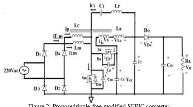
Figure 2: Proposedripple-free modified SEPIC converter
In proposed SEPIC converter, auxiliary switch and a clamp capacitor are added. The both inductorare utilized toobtain ripple-free input current and achieve ZVS operation of the mainand auxiliary switches.The proposed converter achieves high efficiency due to soft-switching characteristics of power semiconductor devices. By utilizing the voltage multiplier technique, voltage stresses of the power switches and diode are reduced by half and the reverse-recovery loss of the output diodeis significantly reduced due to the resonance between the resonant inductor and the capacitor in the multiplier circuit.
II. ANALYSIS AND CIRCUIT CONFIGURATION OF PROPOSED CONVERTER
The conventional SEPIC converter is shown in Fig. 1. The circuit diagram of the proposed ripple-free modified SEPIC converter is shown in Fig. 2. In the proposed converter, the resonant inductor Lr and the active clamp cell consisting of the auxiliary switch Sa and the clamp capacitor Cc are added to the conventional SEPIC converter. The coupled inductor Lc is modeled as the magnetizing inductance Lm and a transformer is high-frequency and made up ofFerrite-core with a turn ratio of 1: 2, 40V and 2A. The diodes Da and Dm are the intrinsic body diodes of the auxiliary switch Sa and the main switch Sm. The capacitors Ca and Cm are their parasitic output capacitances. The duty ratio D is based on the main switch Sm and the switches Sa and Sm are operated asymmetrically. To simplify the steady-state analysis, it is assumed that those capacitors C1, Cc, and Co have large values and the voltage ripples across them can be ignored. The magnetizing inductance current iLm is approaching to its minimum value and the auxiliary inductor current iLa is approaching to its maximum value. And the output diode is not conducting.
2.1 Soft-Switching Operation
The auxiliary switch Sa is turned OFF. Then, the energy stored in the magnetic components such as Lm, Lr and La starts to charge Ca and discharge Cm. Therefore, the voltage Vsa across the auxiliary switch Sa starts to rise from zero and the voltage vSm across the main switch Sm starts to fall from Vcc. Then, the body diode Dm is turned ON. After that, the gate signal is applied to the switch Sm and the channel of Sm takes over the current flowing through Dm. Since the voltage Vsm is clamped as zero with turn-on of Dm before the switch Sm is turned ON, zero-voltage turn-on of Sm is achieved.
ISSN(E): 2277-128X, ISBN: 978-93-87396-07-4, pp. 373-381
The input voltage is applied toLm and the current iLm increases linearly from its minimum value. The main switch Sm is turned OFF. Then, the voltage Vsm increases and the voltage decreases from Vcc at the same time due to the energy stored in themagnetic components.Then,the body diode Da turned ON. After that, the gate signal isapplied to the switch Saand the channel of Sa takes over the current flowing through Da. Since the voltage Vsa clamped as zero before the switch Sa turned ON, zero-voltage turn-onofSaachieved.With the turn-onSa, the output diode Da starts to conduct.Then the resonance occurs between the resonant inductor Lr and the capacitor C1.
The output diode current decreases and the zero-current turn OFF of the diode Doare achieved. Since the current changing rate of Do is controlledby a resonant manner, its reverse-recovery problem is reduced.
III. DESIGN PARAMETER 3.1 INPUT CURRENT RIPPLE
The input current 𝑖𝑖𝑛 given by
𝑖𝑖𝑛 𝑡 = 𝑖𝐿𝑚 𝑡 + 𝑖𝑝 𝑡 (1)
The ripple component of 𝑖𝑖𝑛can be removed by satisfying the following condition:
𝐿 𝑎+ 𝐿𝑟 = 𝑛 1 − 𝑛 𝐿𝑚 (2)
Where, n is turns ratio. Under the condition of (2), the input current 𝑖𝑖𝑛is constant.
3.2 ZVS CONDITION
The ZVS condition for 𝑆𝑎is given by
𝐼𝐿𝑚 1− 1 − 𝑛 𝐼𝐿𝑎2> 0 (3)
Since 𝐼𝐿𝑚1 is always positive and 𝐼𝐿𝑎2is always negative for n <1, the condition of (3) is always satisfied for n <1. Therefore, the ZVS of 𝑆𝑎is always achieved.
Similarly, for the ZVS condition for 𝑆𝑚, the following condition should be satisfied
−𝐼𝐿𝑚 2+ 1 − 𝑛 𝐼𝐿𝑎1> 0 (4)
𝑉𝐷𝑜 ,𝑚𝑎𝑥 = 𝑉𝑜+(1 − 𝑛)𝑉𝑖𝑛𝐿𝑎
𝐿𝑎+ 𝐿𝑟 + 𝑛𝑉𝑖𝑛− 𝑉𝐶𝑐 (5)
IV. DESCRIPTION OF A PROPOSED CONVERTER
Figure 4:Simulated Block Diagram of SEPIC with Motor load.
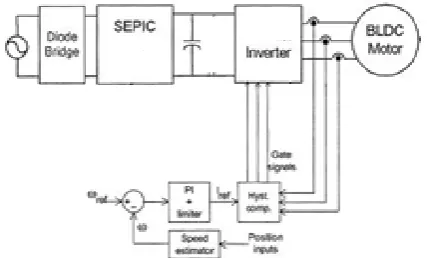
Figure 5: Basic BLDC motor control system with position sensors
ISSN(E): 2277-128X, ISBN: 978-93-87396-07-4, pp. 373-381
resistance. This makes parallel operation of MOSFET easy. In MOSFET secondary break down does not occur, because it has positive temperature co-efficient. Powers MOSFET in higher voltage rating has more conduction losses.The chosen MOSFET is IRF 840 and voltage and current rating is 500V and 8A. All the power MOSFETs are designed for application such as switching regulators, switching converters, motor drives.The IRF-840 provides fast switching, ruggedized device design, low on-resistance and cost effectiveness, dynamic dv/dt rating, repetitive avalanche rated and ease of paralleling.The hardware implementation includes Power circuit and Control circuit.
Figure 6: Hardware Block Diagram of SEPIC with Motor load
The figure of the drive system implementation is given in Fig.5. AC supply is rectified using diode bridge and changed to DC supply. The dc bus voltage is regulated by PWM of the switch S1. This DC power is regulated using SEPIC. This DC-DC converter is applied to minimize the harmonics in the input current. Then the DC power is supplied to BLDC motor through inverter. Hysteresis control is used to observe the phase currents to the reference current. The rotor position is detected by hall sensors, and the position information is used to determine the phase winding to be excited. The speed of the motor is derived from the position inputs and is compared with the speed reference to create the current references The motor shaft is coupled to a hysteresis brake acting as a load. It provides isolation between microcontroller and power circuits. RPS gives 5V supply for micro controller and 12V supply for driver. It is converted from AC supply. AC supply is step down using step down transformer.A capacitive filter circuit is used where a capacitor is connected at the rectifier output and dc is obtained across it. The filtered waveform is essentially a dc voltage with negligible ripple and it is ultimately fed to the motor load.
4.1 Power circuit
The 230/12V AC input is rectified into 16V pulsating DC with the help of full bridge rectifier circuit.
Figure 7: Circuit Diagram of Power Circuit
The ripples in the pulsating DC are removed and pure DC is obtained by using a capacitor filter.The positive terminal of the capacitor is connected to the input pin of the 7812 regulatorfor voltage regulation. An output voltage of 12V obtained from the output pin of 7812 is fed as the supply to thepulse amplifier.An output voltage of 5V obtained from the output pin of 7805 is fed as the supply to the microprocessor.From the same output pin of the 7805, a LED is connected in series with the resistor toindicate that the power is ON.
4.2 Control circuit
The control circuit controls the power circuit by using gate pulses generated by controller.The control circuit has the following Power supply,Microcontroller,Driver circuit (Isolation circuit).
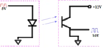
The driver unit consists of optocoupler and isolation circuit. There are many situations where signals and data need to be transferred from onesubsystem to another within a piece of electronics equipment, or from one piece of equipment toanother, without making a direct ohmic electrical connection. Often this is because the sourceand destination are (or may be at times) at very different voltage levels, like a microprocessorwhich is operating from 5V DC but being used to control a MOSFET which is switching 240VAC. In such situations the link between the two must be an isolated one, to protect themicrocontroller from over voltage damage.
ISSN(E): 2277-128X, ISBN: 978-93-87396-07-4, pp. 373-381
Optocoupler is an electronic device designed to transfer electrical signals by utilizinglight waves to provide coupling with electrical isolation between its input and output. The mainpurpose is to prevent high voltages from damaging components or distorting transmissions onthe other side. An opto-isolator contains a source (emitter) of light, almost a LED that convertselectrical input signal into light, and a photo sensor, which detects incoming light and either,generates electric energy directly.
Figure 8: Circuit Diagram of Driver circuit
The driver is a high voltage, high speed power MOSFET driver with independent high andlow side referenced output channels.Logic inputs are compatible with standard output, down to 3.3V logic. The output drivers feature a high pulse current buffer stagedesigned for minimum driver cross-conduction.Some of the special features of are floating channel designed for bootstrap operation, gate drive supply range from 10 to 20V, under voltage lockout for both channels, CMOS Schmitt-triggered inputs with pull down, cycle by cycle edge-triggered shutdown logic, matched propagation delay for both channels.
Figure 9: Circuit Configuration of Proposed SEPIC converter
The figure 9shows the circuit configuration of Diode Bridge rectifier, Capacitor, SEPIC converter, PI Controller with closed loop DC Motor load. The given input is ac and it is rectified into dc by rectifier for sepic converter to drive the dc shunt motor.
V. SIMULATION RESULT AND DISCUSSION
ISSN(E): 2277-128X, ISBN: 978-93-87396-07-4, pp. 373-381
Figure 10: Input and Output Voltage Waveform
The converter with motor Load is simulated at various load conditions in order to obtain maximum voltage. The main objective to drive a D.C. Motor to attain twice that of an input voltage of the system. The current is predicated at all the loaded conditions. The results obtained in the form of waveform are withrespect to the time. The figure 10 shows the output voltage. The output voltage is observed to be35V.
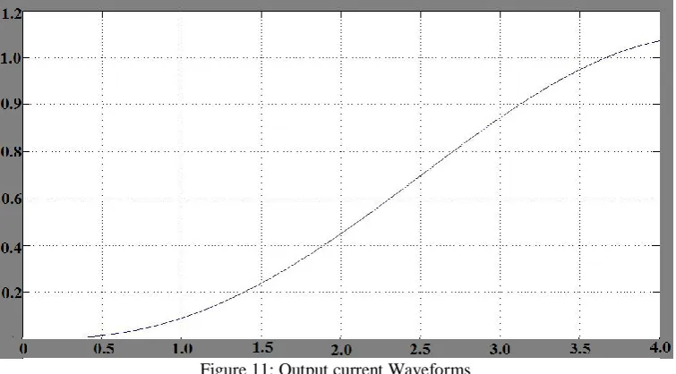
Figure 11: Output current Waveforms
The figure11 shows the output current of D.C. Motor and it is 1.1A for the given input voltage17Vdc.
VI. EXPERIMENTAL RESULT
To verify performance and analysis of the proposed SEPIC converter, a prototype is implemented and tested with the following specification.
1) Input voltage Vin = 17V. 2) Output voltage Vo = 35V. 3) Switching frequency fs = 33 kHz. 4) Output power Po = 55W.
ISSN(E): 2277-128X, ISBN: 978-93-87396-07-4, pp. 373-381
Figure 12: Overall view of Hardware Kit
ISSN(E): 2277-128X, ISBN: 978-93-87396-07-4, pp. 373-381
Figure 14: Comparison of simulated and hardware Voltage for motorload
The variations are very small which relates the characteristics of the converter more close between the simulation and the hardware results. The proposed converter shows better characteristics due to its soft-switching of power switchesand the output diode.
Figure 15.Efficiency vs Output Power of motorload
The SEPICconverter fed DC Motor attains an efficiency of 94.5% at full load condition. The proposed converter exhibit higher efficiencydue to its soft-switchingcharacteristics of power switchesand the output diode. The converter shows lower efficiency under light load. This is due to MOSFET’s secondary current. It increases the conduction loss and alsothe powerloss at light load.
VII. CONCLUSION
The operating principle, analysis, and the implementation of a SEPIC converter with soft-switching are presented in this paper. In the proposed converter,the coupled inductor and power switchesaremainly used for ripple-free input current and to achieve ZVS operation. The advantages of the proposed converter are low voltage stresses, low switching losses, reverse-recovery problem of theoutput diode, and high-voltage applications. The design consideration ofthe proposed converter is included. The experimental results based on a prototype are presented for validation.
REFERENCES
[1] J.M. Kwon, W.Y. Choi, J.J. Lee, E.H. Kim and B.H. Kwon, 2006, “Continuous-conduction-mode SEPIC converter with low reverserecovery loss for power factor correction,” IET Proc. Electr. Power Appl., vol. 153, no. 5, pp. 673–681.
ISSN(E): 2277-128X, ISBN: 978-93-87396-07-4, pp. 373-381
[3] P. F.Melo, R. Gules, E. F. R. Romaneli, and R. C.Annunziato, 2010, “A modified SEPIC converter for high-power-factor rectifier and universal input voltage applications,” IEEE Trans. Power Electron., vol. 25, no. 2, pp. 310–321.
[4] J. C. W. Lam and P. K. Jain, 2010,“A high-power-factor single-stage singleswitch electronic ballast for compact fluorescent lamps,” IEEE Trans. Power Electron., vol. 25, no. 8, pp. 2045–2058.
[5] H.-J. Chiu, Y.K. Lo, J.-T. Chen, S.J. Cheng, C.Y. Lin and S.C. Mou, 2010 “A high-efficiency dimmable LED driver for low-power lighting applications,” IEEE Trans. Ind. Electron., vol. 57, no. 2, pp. 735–743.
.
AUTHOR’S BIOGRAPHY
P. Dhanasekaran is currently working in Sri Venketesa Perumal College of Engineering and Technology, JNTU, Anantapur and born in Chennai, Tamil Nadu, India.. He received his M.E Degree from Jeppiaar Engineering College, Anna University, Chennai, India. He received his B.E degree in Electrical and Electronics Engineering in Loyola institute of technology, Anna University, Chennai, India in 2011.His current research interests include sepic topology, Induction Motor Drives, Multi-level inverter, soft-switching techniques, Fuzzy logic in image processing, Z-Source Converters. He published more than 10 papers in proceedings/national conference/International conference/journals. His mail id
S.Shanmugam received his M.E Degree from PSG college of Technology, Anna University, Coimbatore, India.. His current research interests include Y-source inverters, High-Frequency MOSFET gate drivers, Induction Motor Drives, Electrical machines, Power electronics, Neural network. His mail id