Application note
Designing a low cost power supply using a
VIPer12/22A-E in a buck configuration
Introduction
Many appliances today use nonisolated power supply to furnish low output power required to run a micro, LED display, and a few relays or AC switches. This type of power supply has a single rectifier so as to reference the neutral to output ground in order to fire TRIACs or AC switches. This article describes the use of the VIPer12A-E and the VIPer22A-E which are pin-for-pin compatible and can supply power for many applications. This paper provides an off-line, nonisolated power supply evaluation board based on the VIPer12/22A-E. Four different examples are covered. The VIPer12A-E is used for 12 V at 200 mA and 16 V at 200 mA. The VIPer22A-E is used for 12 V at 350 mA and 16 V at 350 mA. The same board can be used for any output voltage from 10 V to 35 V. For outputs less than 16 V, D6 and C4 are populated and W1 is omitted. For outputs greater than 16 V, D6 and C4 are omitted and W1 is populated. For more design detail, see AN1357 "VIPower: low cost power sullies using the VIPer12A-E in nonisolated application." The objective of this application note is to familiarize the end user with this reference design and to quickly modify it for different voltage output. This design gives:
■ Lowest possible component count
■ Integrated thermal overload protection
■ About 200 mW at no-load consumption
■ Efficiency measured between 70% to 80% at full load
■ Integrated Short circuit protection
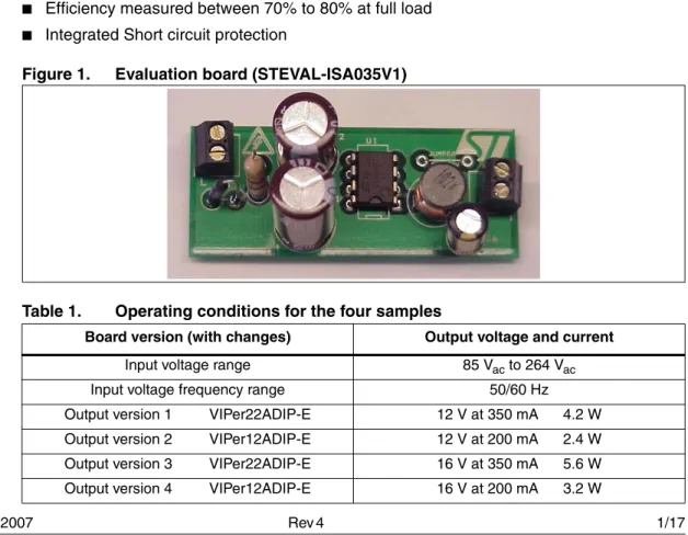
Figure 1. Evaluation board (STEVAL-ISA035V1)
Table 1. Operating conditions for the four samples
Board version (with changes) Output voltage and current
Input voltage range 85 Vac to 264 Vac
Input voltage frequency range 50/60 Hz
Output version 1 VIPer22ADIP-E 12 V at 350 mA 4.2 W Output version 2 VIPer12ADIP-E 12 V at 200 mA 2.4 W Output version 3 VIPer22ADIP-E 16 V at 350 mA 5.6 W Output version 4 VIPer12ADIP-E 16 V at 200 mA 3.2 W
Contents
1
Circuit operation . . . 4
1.1
Input line rectification and line conducted filter . . . 4
1.2
Start circuit . . . 4
1.3
Inductor selection . . . 5
1.4
Design example . . . 5
1.5
Design hints and trade-off . . . 5
1.6
Board layout . . . 9
1.7
Burst mode in no-load or very light load . . . 11
1.8
Short circuit . . . 12
1.9
Performance . . . 13
1.10
EMI conducted . . . 15
2
Conclusion . . . 16
List of figures
Figure 1. Evaluation board (STEVAL-ISA035V1) . . . 1
Figure 2. Inductor current: 470 µH VS 1000 µH. . . 6
Figure 3. Schematic for 12 V at 350 mA . . . 7
Figure 4. Schematic for 16 V at 350 mA . . . 8
Figure 5. Composite. . . 9
Figure 6. Top side . . . 9
Figure 7. Bottom side and surface mount components (viewed from top). . . 9
Figure 8. Bad start . . . 11
Figure 9. Good start . . . 11
Figure 10. Burst mode . . . 12
Figure 11. Operation during a short . . . 12
Figure 12. Load regulations for 12 V output. . . 14
Figure 13. Line regulation . . . 14
Figure 14. Efficiency . . . 15
Figure 15. VIPer22-E, 12 V at 350 mA output . . . 15
Figure 16. VIPer12-E, 12 V at 200 mA output . . . 15
Figure 17. VIPer22-E, 16 V at 350 mA output . . . 16
1 Circuit
operation
1.1
Input line rectification and line conducted filter
The circuit operations for all four versions are basically the same. The difference is in the circuit for startup. Version 1 will be described here with reference toFigure 3. The output of the converter is not isolated from the input. This makes neutral common to output ground thus giving a reference back to neutral. The buck is less expensive due to the fact that it does not use a transformer and an opto coupler. The AC line is applied through D1 which rectifies the line input every other half cycle.
C1, L0, C2 form a pie filter to reduce EMI noise. The value of the capacitor is chosen to maintain a reasonable valley, because the caps are charged every other half cycle. Two diodes can be used in place of D1 to sustain burst pulses of 2 kV. R10 serves two purposes, one is for inrush limiting and the other is to act as a fuse in case of a catastrophic failure. A wire wound resistor handles the energy of the inrush. Flame proof resistor and a fuse can be used depending on system and safety requirements. C7 helps the EMI by balancing line and neutral noise without using an Xcap. This will pass EN55022 level "B". If the requirement is less, then this cap can be left out of the circuit.
1.2 Start
circuit
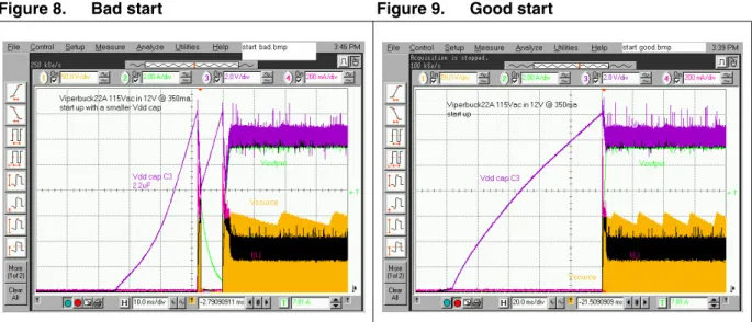
The voltage across C2 is fed to the drain, pin 5 through 8. Inside the VIPer, the constant current source delivers 1mA to the Vdd pin 4. This current charges C3. When the voltage on the Vdd pin reaches 14.5 V nominal, the current source turns off and the VIPer starts pulsing. During this time, the energy is being supplied from the Vdd cap. The energy stored must be greater than the energy needed to supply the output current plus the energy to charge of the output capacitor, before the Vdd cap falls below 9 V. This can be seen in
Figure 8 and Figure 9. The value of the capacitor is therefore chosen to accommodate the startup time. During a short circuit, the Vdd cap discharges below the minim value enabling the internal high voltage current generator to initiate a new startup sequence. The charging and discharging of the capacitor determine the time period that the power supply is to be on and off. This reduces the RMS heating effect on all components. The regulation circuit consists of Dz, C4 and D8. D8 peak charges C4 during the freewheeling time when D5 is conducting. During this time, the source or reference to the VIPer is one diode drop below ground, which compensates for the D8 drop. So basically the Zener voltage is the same as the output voltage. C4 is connected across Vfb and source to filter the regulation voltage. Dz is a BZT52C12, ½ W Zener with a specified test current of 5 mA. These Zeners that are specified at a lower current give better accuracy of the output voltage. If the output voltage is lower than 16 V, the circuit can be configured as in Figure 3 where Vdd is separated from the Vfb pin. When the internal current source charges the Vdd cap, Vdd can reach 16V at worse case condition. A 16 V Zener with a 5% low tolerance can be 15.2 V plus the internal resistance to ground is 1230 Ω which is an additional 1.23 V for a total of 16.4 V. For 16 V output and higher, the Vdd pin and the Vfb pin can share a common diode and capacitor filter similar toFigure 4.
1.3 Inductor
selection
A starting point for the inductor operating in discontinuous mode can be derived from the following formula which gives a good approximation of the inductor.
Equation 1
Where Idpeak is the minimum peak drain current, 320 mA for the VIPer12A-E and 560 mA for
the VIPer22A-E, f is the switching frequency at 60 kHz. The maximum peak current limits the power delivered in the buck topology. Therefore, the calculation above is for an inductor that operates in discontinuous mode. If the current swings down to zero, than the peak current is twice the output. This limits the output current to 280 mA for a VIPer22A-E. If the inductor is a larger value, operating between continuous and discontinuous mode, we can reach 200 mA comfortably away from the current limit point. C6 has to be a low ESR capacitor to give the low ripple voltage
Equation 2
D5 needs to be a fast recovery diode but D6 and D8 can be standard diodes. DZ1 is used to clamp the voltage to 16 V. The nature of the buck topology is to peak charge at no-load. A Zener 3 to 4 V higher than the output voltage is recommended.
1.4 Design
example
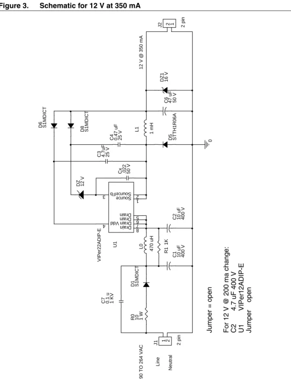
Figure 3 is the schematic for the evaluation board. It is set up for 12 V with a maximum current of 350 mA. If less current is required, then the VIPer22A-E can be changed to a VIPer12A-E and C2 can be decreased from 10 µf to 4.7 µF. This delivers up to 200 mA.
Figure 4shows the same board but for 16 V output or higher, D6 and C4 can be left out. The jumper bridges the output voltage to the Vdd pin.
1.5
Design hints and trade-off
The value of L determines the boundary condition between continuous and discontinuous mode for a given output current. In order to operate in discontinuous mode, the inductor value has to be lower than
Equation 3
Where R is the load resistance, T is the switching period, and D is the duty cycle. There are two points to consider. One is, the more discontinuous the higher the peak current. This point should be kept lower than the minimum pulse by pulse current limit of the VIPer22A-E which is 0.56 A. The other is if we use a larger value inductor to run continuous all of the time, we run into excess heat from switching losses of the MOSFET inside the VIPer. Of course, the inductor current rating must be higher than the output current to prevent the risk of saturating the core.
L 2 Pout
Idpeak
( )2
f
•
---•
=
Vripple = Iripple•Cesr
L 1
2
---•R•T•(1–D) =
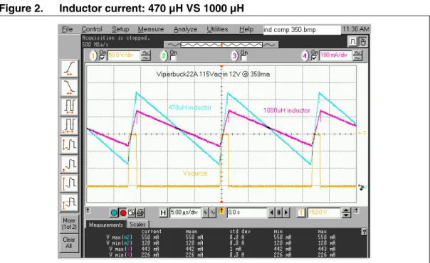
Figure 2. Inductor current: 470 µH VS 1000 µH
The blue trace is the current with 470 µH inductor and the purple trace is the current with a 1000 µH inductor.
On the above scope plot in Figure 2, the trace represents the current going through the inductor. Current charges up the inductor during the time the MOSFET is on. At this time, the source pin is the same as the rectified line input and the current is ramping up. At 350 mA output current, the peak of the current is 550 mA for a 470 µH inductor, the blue trace. The worse case condition for the VIPer Idlim is 560 mA. So therefore we are close to the pulse by pulse current limit trip point. This is manifested by the output voltage dropping as the output current is being raised past the limit. 470 µH inductor is the minimum value that can be used from the calculations for a 350 mA output. A good compromise is a 1000 µH making the swing less, keeping the peak at 443 mA, away from the 560 mA current limit. Looking at the purple trace the turn-on losses are increased and the turn-off losses are decreased in the MOSFET inside the VIPer.
It is best to choose the inductor to give ½ the ripple current between discontinuous to continuous. This is the best compromise when working close to the maximum current. The trade-off is a little more heat for the safety margin away from the current trip point.
VIPer temperature rise with two different inductors at 350 mA is:
Table 2. VIPer temperature rise with different inductors
Inductor Maximum peak current VIPer22ADIP-E temperature rise
470 µH 550 mA 34 °C
Figure 3. Schematic for 12 V at 350 mA
Neutra
l
Li
ne
DZ 12 V
L0 470 u
H
L1 1 mH C6 47 uF 50 V
Cx .022 50 V
C2 10 uF 400 V
C1 10 uF 400 V
R0 10 1 W
R1
1K
90 TO 264 V
A C 12 V @ 35 0 mA D1 S1MDIC T D8 S1MDIC T
D5 ST
TH1R06A D6 S1MDIC T U1 VIP er22 A DIP-E Drain 8 Drain 6 Drain 7 Drain 5 Source 1 Source 2 Fb 3 Vdd 4
DZ1 16 V
For
12 V @
200 ma chan g e : C 2 4.7 uF 400 V U1 VI Per12ADIP-E Jumper ope n 0
J1 2 pi
n
1 2 J2 2 pi
n 1 2 Jumper = ope n
C7 0.1 u 1 K
V
C3 4.7uF 25 V C4 0.47 uF 25 V
Figure 4. Schematic for 16 V at 350 mA
DZ 16V 1N
5246 U1 VI P e r 2 2 ADIP-E Drain 8 Drain 6 Drain 7 Drain 5 Sour ce 1 Sour ce 2 Fb 3 Vdd 4
L0 470 u
H
L1 1 m
H
C6 47 u
F
50 V
Cx .022
C2 10 u
F
400 V
C1 10 u
F
400 V
R0 10 1 W
R1 1 K 90 TO 264 VAC
16 V @
350 m A D1 S1 M D I C T D8 S1 M D I C T D5 STTH 1R 0 6 A ST Lin e Ne utral
DZ1 20 V
F o r 16 V @ 200 m a change : C 2 4.7 uF 400 V U 1 V IPe r12 AD IP -E Jump er = S h ort circuit 0
J2 2 p
i 1 2 J1 2 pin 1 2 C7 0.1 u 1 KV C3 4.7 u F 25 V
1.6 Board
layout
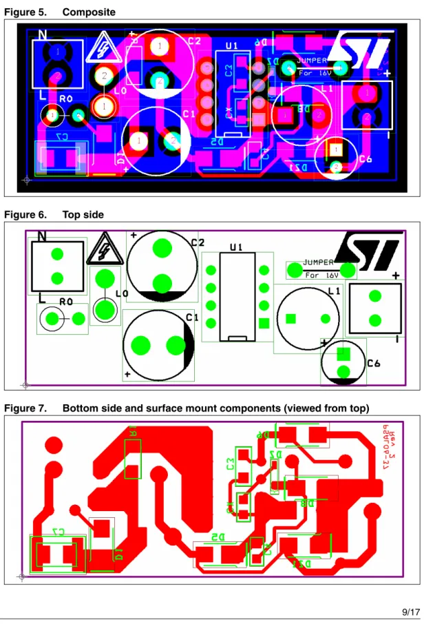
A composite view of the board shows a double-sided board with surface mount components on the bottom. The top is a ground plane which helps with EMI. The actual measurements of the PC board are 55 mm by 23 mm.
Figure 5. Composite
Figure 6. Top side
The above board can be modified to any voltage output from 10 V to 15 V by changing DZ. To modify the board to 16 or higher, D6 and C4 can be omitted and the jumper wire can be installed. For 16 V operation or higher, Vdd and Vf can share the same source without having the current leak through the Zener and Vf pin path. The output voltage can be changed by changing DZ from 16 V Zener to a higher value matching the output voltage. If less current is required, the board can be changed with a VIPer12A-E dip which is pin-for
-pin compatible with the VIPer22ADIP-E.
Table 3. Bill of material for VIPer22A-E Buck 12 V at 350 mA
Item Qty Ref. Part V/W Description CAT#
1 1 Cx 0.022 50 V X7R +/-10% GP SM Ceramic
2 2 C1,C2 10 µF 400 V 105 C UCC
EKMG401ELL100MJ20S
3 1 C3 4.7 µF 25 V X7R +/-10% TDK C3216X7R1E475K
4 1 C4 0.47 µF 25 V X7R +/-10% TDK C2012X7R1E474K
5 1 C6 47 µF 50 V 105 C Low ESR Low ESR
6 1 C7 0.1 µ 1 kV X7R +/-15% Murata
GRM55DR73A104KW011
7 1 DZ 12 V zener BZT5212FDICT
8 1 DZ1 16 V zener BZT5216FDICT
9 3 D1,D6,D8 S1MDICT SM GP Diode 1 kV 1 A S1MD
10 1 D5 STTH1R06A 600 V 1 A Ultrafast STMicroelectronics
11 2 J1, J2 2 pin Mouser 651-1751099
12 1 L0 470 µH 140 mA JW Miller 5300-33
13 1 L1 1 mH 400 mA Compostar Q3277 or
JW Miller RL895-102K
14 1 R0 10 Ω 1 W wire wound ALSR1J-10
15 1 R1 1 kΩ 5% SM 1206 CERAMIC
16 1 U1 VIPer22ADIP-E STMicroelectronics
Table 4. Bill of material for VIPer22A-E Buck 16 V at 350 mA
For 16 V or higher operation.
Omit 1 D8 S1MDICT SM GP Diode
1 kV 1A S1MD
Omit 1 C4 0.47 µF 25 V X7R +/-10% TDK C2012X7R1E474K
The VIPer internal 1 mA current source charges up the Vdd capacitor. When the voltage on the Vdd pin reaches the Vdd startup threshold (Worse case is 13 V) the VIPer starts pulsing, raising the output voltage to the point of bootstrapping. The Vdd capacitor needs to supply the energy to supply the necessary output current and to charge up the output capacitor, before the Vdd voltage falls below the Vdd under voltage shutdown threshold (worse case is 9 V). Figure 8 and 9 show a Vdd cap that is not large enough to start up the evaluation board under a resistive load of 350 mA.
InFigure 8 the purple trace is the Vdd voltage rising to ~14 V. The energy with the 2.2 µF
capacitor does not store enough energy. As seen the output voltage (green trace) does not reach high enough to bootstrap, It succeeds the second time after there is a partial charge on the output cap. Figure 9 is using a 4.7 µF Vdd cap. With adequate energy the power
supply starts the first time.
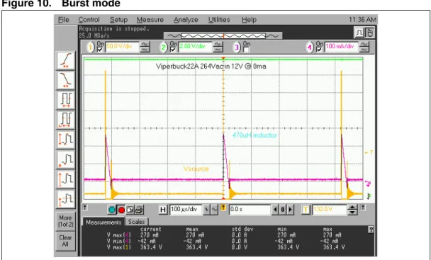
1.7
Burst mode in no-load or very light load
At very light load, the on-time becomes so small that some pulses are skipped in order to stay in regulation and meet energy requirements such as Blue Angel or Energy Star. This mode is called burst mode. It skips as many cycles as needed to maintain regulation. In the case below at no-load about 9 cycles are skipped to maintain an output.
Figure 8. Bad start Figure 9. Good start
Figure 10. Burst mode
1.8 Short
circuit
The VIPer has pulse-by-pulse current limit. When the current ramps up to the current limit, the pulse is terminated. This is manifested by reducing the output voltage as the current is increased. The voltage decreases until it falls below the undervoltage shutdown threshold of 9 V, (pin4). During a short circuit the VIPer turns on and off. When the Vdd reaches the starting voltage, the current is limited by the pulse-by-pulse current limit. The voltage falls to the undervoltage shutdown point and the cycle repeats itself at a 16% duty cycle. This reduces the RMS current going through the circuit as seen inFigure 11.
1.9 Performance
Regulation for the VIPer22A-E and VIPer12A-E can be seen below. Keep in mind that the buck topology will peak charge at zero load. DZ1 will clamp the voltage to 3 - 4 V above the output. Load regulation is taken from 0.03 A to 0.35 A.
Note: The following measurements were taken on the appropriate version of the boards. Discrepancy of measurements can be present, which is to be expected due to the 5% tolerance of the Zener and equipment used for the measurements. The measurements shown are at room temperature. If higher operating temperatures are used, current loads must be adjusted accordingly.
Table 5. VIPer22ADIP-E, 12 V at 350 mA
VIPer22 buck 12 V / 350 mA
Vin 12 V load 12 V W in Efficiency
90 Vac 0 15.81 0.12
90 Vac 0.03 12.58 0.45
90 Vac 0.35 11.7 5.64 72.6%
264 Vac 0.35 12.21 6.12 69.8%
MIN 11.7
MAX 12.58
DELTA 0.88
Line reg. 6.0%
+/- % load reg (.03 to max) 3.8%
Ripple mv pp at 120 Vac 52
Blue Angel at no-load at 115 Vac in W 0.12
Short circuit ok
Table 6. VIPer12ADIP-E, 12 V at 200 mA
VIPer12 buck 12 V / 200 mA #1
Vin 12 V load 12 V W in Efficiency
90 Vac 0 15.6 0.15
90 Vac 0.03 12.7 0.495
90 Vac 0.2 11.85 3.06 77.5%
264 Vac 0.2 12.1 3.25 74.5%
MIN 11.85
MAX 12.7
DELTA 0.85
Line Reg. 2.9%
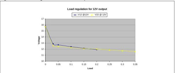
12 V output load regulation for VIPer12-E and VIPer22A-E is shown in Figure 12.
Figure 12. Load regulations for 12 V output
Line regulation shown at three different current levels: 100 mA, 200 mA, and 350 mA.
Figure 13. Line regulation
Ripple mv pp at 120 Vac 50
Blue Angel at no-load at 115 Vac in W 0.15
Short circuit ok
Table 6. VIPer12ADIP-E, 12 V at 200 mA (continued)
VIPer12 buck 12 V / 200 mA #1
Vin 12 V load 12 V W in Efficiency
Load regulation for 12V output
10 11 12 13 14 15 16 17
0 0.05 0.1 0.15 0.2 0.25 0.3 0.35
Load
Vo
lt
a
g
e
V12 @12V V22 @ 12V
Line regulation
11 11.2 11.4 11.6 11.8 12 12.2 12.4 12.6 12.8 13
80 130 180 230
Line Voltage
O
u
tp
u
t V
o
lt
a
g
e
Figure 14. Efficiency
Efficiency is about 75% at 120 Vac. Efficiency is better at higher output voltages.
1.10 EMI
conducted
EMI was checked for all four versions for maximum peak reading.
Efficiency VS Input Line for 12V output
60% 65% 70% 75% 80% 85%
80 100 120 140 160 180 200 220 240 260 Input Line
E
ff
ici
en
cy
effic. @ 100ma effic. @ 200ma effic. @ 350ma
Figure 15. VIPer22-E, 12 V at 350 mA output Figure 16. VIPer12-E, 12 V at 200 mA output
2 Conclusion
Using the VIPer in the buck mode has its benefits for appliances and other industrial equipment which require a reference to neutral. For currents up to 350 mA and voltages greater than 10 V, it is beneficial to use this inexpensive power supply. The cost savings compared to a transformer, opto-coupler, and low parts count, makes this solution very attractive.
3 Revision
history
Figure 17. VIPer22-E, 16 V at 350 mA output Figure 18. VIPer12-E, 16 V at 200 mA output
Table 7. Document revision history
Date Revision Changes
06-Jul-2007 1 First issue
13-Sep-2007 2 – Note added in Section 1.9: Performance – Minor text changes
21-Sep-2007 3 Modified: Figure 1
Please Read Carefully:
Information in this document is provided solely in connection with ST products. STMicroelectronics NV and its subsidiaries (“ST”) reserve the right to make changes, corrections, modifications or improvements, to this document, and the products and services described herein at any time, without notice.
All ST products are sold pursuant to ST’s terms and conditions of sale.
Purchasers are solely responsible for the choice, selection and use of the ST products and services described herein, and ST assumes no liability whatsoever relating to the choice, selection or use of the ST products and services described herein.
No license, express or implied, by estoppel or otherwise, to any intellectual property rights is granted under this document. If any part of this document refers to any third party products or services it shall not be deemed a license grant by ST for the use of such third party products or services, or any intellectual property contained therein or considered as a warranty covering the use in any manner whatsoever of such third party products or services or any intellectual property contained therein.
UNLESS OTHERWISE SET FORTH IN ST’S TERMS AND CONDITIONS OF SALE ST DISCLAIMS ANY EXPRESS OR IMPLIED WARRANTY WITH RESPECT TO THE USE AND/OR SALE OF ST PRODUCTS INCLUDING WITHOUT LIMITATION IMPLIED WARRANTIES OF MERCHANTABILITY, FITNESS FOR A PARTICULAR PURPOSE (AND THEIR EQUIVALENTS UNDER THE LAWS OF ANY JURISDICTION), OR INFRINGEMENT OF ANY PATENT, COPYRIGHT OR OTHER INTELLECTUAL PROPERTY RIGHT. UNLESS EXPRESSLY APPROVED IN WRITING BY AN AUTHORIZED ST REPRESENTATIVE, ST PRODUCTS ARE NOT RECOMMENDED, AUTHORIZED OR WARRANTED FOR USE IN MILITARY, AIR CRAFT, SPACE, LIFE SAVING, OR LIFE SUSTAINING APPLICATIONS, NOR IN PRODUCTS OR SYSTEMS WHERE FAILURE OR MALFUNCTION MAY RESULT IN PERSONAL INJURY, DEATH, OR SEVERE PROPERTY OR ENVIRONMENTAL DAMAGE. ST PRODUCTS WHICH ARE NOT SPECIFIED AS "AUTOMOTIVE GRADE" MAY ONLY BE USED IN AUTOMOTIVE APPLICATIONS AT USER’S OWN RISK.
Resale of ST products with provisions different from the statements and/or technical features set forth in this document shall immediately void any warranty granted by ST for the ST product or service described herein and shall not create or extend in any manner whatsoever, any liability of ST.
ST and the ST logo are trademarks or registered trademarks of ST in various countries. Information in this document supersedes and replaces all information previously supplied.
The ST logo is a registered trademark of STMicroelectronics. All other names are the property of their respective owners.
© 2007 STMicroelectronics - All rights reserved
STMicroelectronics group of companies
Australia - Belgium - Brazil - Canada - China - Czech Republic - Finland - France - Germany - Hong Kong - India - Israel - Italy - Japan - Malaysia - Malta - Morocco - Singapore - Spain - Sweden - Switzerland - United Kingdom - United States of America