A Low-Power, Variable-Resolution
Analog-to-Digital Converter
By
Carrie Aust
Thesis Submitted to the Faculty
of the Virginia Polytechnic Institute and State University in partial fulfillment of the requirements for the degree of
Master of Science In
Electrical Engineering Dr. Dong S. Ha, Chair Dr. Peter M. Athanas
Dr. Jeffrey H. Reed
June 16, 2000 Blacksburg, Virginia
Keywords: Analog-to-digital converter, ADC, Low power, Variable resolution Copyright2000 Carrie Aust
A Low-Power, Variable-Resolution
Analog-to-Digital Converter
Carrie Aust
Dr. Dong S. Ha, Chairman
Bradley Department of Electrical and Computer Engineering (Abstract)
Analog-to-digital converters (ADCs) are used to convert analog signals to the digital domain in digital communications systems. An ADC used in wireless
communications should meet the necessary requirements for the worst-case channel condition. However, the worst-case scenario rarely occurs. As a consequence, a high-resolution and subsequently high power ADC designed for the worst case is not required for most operating conditions. A solution to reduce the power dissipation of ADCs in wireless digital communications systems is to detect the current channel condition and to dynamically vary the resolution of the ADC according to the given channel condition. In this thesis, we investigated an ADC that can change its resolution dynamically and, consequently, its power dissipation. Our ADC is a switched-current, redundant signed-digit (RSD) cyclic implementation that easily incorporates variable resolution.
Furthermore, the RSD cyclic algorithm is insensitive to offsets, allowing simple, low-power comparators. Our ADC is implemented in a 0.35 µm CMOS technology with a single-ended 3.3 V power supply. Our ADC has a maximum power dissipation of 6.35 mW for a 12-bit resolution and dissipates an average of 10 percent less power when the resolution is decreased by two bits. Simulation results indicate our ADC achieves a bit rate of 1.7 MHz and has a SNR of 84 dB for the maximum input frequency of 8.3 kHz.
Acknowledgements
I am indebted to my committee chairman and advisor Dr. Dong S. Ha for giving me the opportunity to work with him. Without his insightful guidance and help, I could not have completed this work. I would also like to express my appreciation to Dr. Peter M. Athanas and Dr. Jeffrey H. Reed for participating in my examination committee.
I greatly appreciate the computing resources provided by VISC (Virginia Tech Information Systems Center). Without these resources, this work could not have been conducted. All the members of the VTVT (Virginia Tech VLSI for
Telecommunications) team have been a great help. I would like to thank Hanbin Kim, Suk Won Kim, Jia Fei, Meenatchi Jagasivamani, and Jos Sulistyo of the VTVT team.
I am very grateful to my family and my fiancé, Douglas H. Cox. Without their encouragement, help, and understanding, completing this work would have been a much more difficult task.
Contents
1 Introduction ... 1
2 Background ... 3
2.1 Introduction ... 3
2.2 Fundamentals of analog-to-digital converters... 3
2.3 Various types of analog-to-digital converter architectures ... 7
2.4 Low-power analog-to-digital converter design approaches ... 9
2.5 Review of contemporary analog-to-digital converters... 10
2.6 Feasibility of variable-resolution analog-to-digital converters ... 12
3 Features of the analog-to-digital converter architecture ... 14
3.1 Introduction ... 14
3.2 Conventional cyclic analog-to-digital converters ... 14
3.2.1 Conventional cyclic conversion algorithm... 15
3.2.2 Offset requirements ... 17
3.3 Redundant signed-digit cyclic analog-to-digital converters... 20
3.3.1 RSD cyclic conversion algorithm ... 21
3.3.2 Offset requirements ... 24
3.3.3 Advantages of the RSD cyclic conversion algorithm ... 29
3.4 Comparator... 29
3.5 Current copiers ... 31
3.5.1 Simple current copier ... 31
3.5.2 Op-amp active current copier... 35
3.5.3 Regulated-cascode current copier ... 37
3.6 Variable resolution ... 39
4 Implementation... 41
4.1 Introduction ... 41
4.2 Architecture of the analog-to-digital converter... 41
4.3 Implementation of the RSD algorithm ... 43
4.3.2 Second phase of the mth bit cycle... 46
4.3.3 First phase of the (m+1)th bit cycle ... 46
4.3.4 Second phase of the (m+1)th bit cycle ... 47
4.3.5 Details of operation ... 47
4.4 Regulated-cascode current copier ... 51
4.4.1 Transistor size considerations ... 51
4.4.2 Operating point... 54
4.4.3 Charge injection considerations ... 58
4.4.4 Current sources... 61
4.4.5 Layout and verification of operation... 62
4.4.6 Implementation of PMOS current copiers ... 64
4.4.7 Dynamic range of the current copiers ... 69
4.5 Regulated-cascode current sources ... 70
4.6 Comparators ... 83
4.7 Input circuit ... 92
4.8 Floor plan of the ADC... 99
4.9 Digital components of the analog-to-digital converter ... 100
4.9.1 Input/output signals ... 100
4.9.2 Overview of operation... 103
4.9.3 Implementation of the switch controller ... 106
4.9.4 Implementation of the resolution controller... 112
4.9.5 Frequency divider... 116
4.9.6 Implementation of the RSD decoder... 117
4.9.7 Floor plan of digital components ... 123
4.10 Standby state ... 124
4.11 Layout considerations ... 128
4.11.1 Process variation issues... 128
4.11.2 Digital noise issues... 131
4.12 Design of the test chip... 131
5.2 Verification of operation ... 138 5.3 Power dissipation ... 140 5.4 Speed ... 143 5.5 Accuracy... 144 6 Conclusion ... 151 6.1 Summary ... 151 6.2 Future improvements... 152 Bibliography ... 154 Vita... 157
List of Figures
Figure 2.1 : Transfer characteristic of an ideal 2-bit ADC... 4
Figure 2.2 : INL error for a 2-bit ADC ... 6
Figure 2.3 : DNL error for a 2-bit ADC... 6
Figure 3.1 : Flow graph for a conventional cyclic conversion algorithm [12]... 15
Figure 3.2 : Robertson diagram of a conventional cyclic ADC [9] ... 17
Figure 3.3 : Robertson diagram of a conventional cyclic ADC with a comparator offset +∆c [9]... 19
Figure 3.4 : Transfer characteristic of a conventional cyclic ADC with a loop offset of +ILSB... 20
Figure 3.5 : Flow graph for the RSD cyclic conversion algorithm [9] ... 22
Figure 3.6 : (a) Robertson diagram of a RSD cyclic ADC for 2P = -2Q = Iref... 24
(b) Robertson diagram of a RSD cyclic ADC for 2P = -2Q = 0 ... 25
(c) Robertson diagram of a RSD cyclic ADC for 2P = -2Q = Iref/2 [9] ... 25
Figure 3.7 : Robertson diagram of a RSD cyclic ADC with a comparator offset +Iref/2 ... 27
Figure 3.8 : Transfer characteristic of the RSD cyclic ADC with a loop offset of +Iref/2... 28
Figure 3.9 : Circuit diagram of a strobed, cross-coupled inverter comparator [9] ... 30
Figure 3.10: A simple current copier [28]... 32
Figure 3.11: Two identical, cascaded simple current copiers [27]... 34
Figure 3.12: An op-amp active current copier [28]... 36
Figure 3.13: A regulated-cascode current copier [28]... 37
Figure 4.1 : Analog-to-digital converter architecture ... 42
Figure 4.3 : (a) Phase one of the mth bit cycle ... 46
(b) Phase two of the mth bit cycle... 46
Figure 4.4 : (a) Phase one of the (m+1)th bit cycle ... 47
(b) Phase two of the (m+1)th bit cycle... 47
Figure 4.5 : (a) Phase one of the first bit cycle ... 48
(b) Phase two of the first bit cycle ... 48
Figure 4.6 : NMOS regulated-cascode current copier... 52
Figure 4.7 : Dummy switch circuit configuration... 59
Figure 4.8 : Current source I of the NMOS regulated-cascode current copier... 61
Figure 4.9 : Layout of the NMOS regulated-cascode current copier... 63
Figure 4.10: Simulation results for the NMOS regulated-cascode current copier... 64
Figure 4.11: PMOS regulated-cascode current copier ... 65
Figure 4.12: PMOS dummy switch circuit configuration... 67
Figure 4.13: Current source I of the PMOS regulated-cascode current copier... 67
Figure 4.14: Layout of the PMOS regulated-cascode current copier... 68
Figure 4.15: Simulation results for the PMOS regulated-cascode current copier... 69
Figure 4.16: NMOS regulated-cascode current source ... 71
Figure 4.17: Layout of the 45 µA NMOS regulated-cascode current sources... 74
Figure 4.18: Layout of the 200 µA NMOS regulated-cascode current source ... 75
Figure 4.19: Simulation results of the 45 µA NMOS regulated-cascode current sources... 76
Figure 4.20: Simulation results of the 200 µA NMOS regulated-cascode current source ... 76
Figure 4.21: Recovery time of the NMOS regulated-cascode current
sources... 77
Figure 4.22: PMOS regulated-cascode current source... 78
Figure 4.23: Layout of the 45 µA PMOS regulated-cascode current sources... 80
Figure 4.24: Layout of the 200 µA PMOS regulated-cascode current source ... 81
Figure 4.25: Simulation results of the 45 µA PMOS regulated-cascode current source ... 82
Figure 4.26: Simulation results of the 200 µA PMOS regulated-cascode current source ... 82
Figure 4.27: Recovery time of the PMOS regulated-cascode current sources... 83
Figure 4.28: Strobed, cross-coupled inverter comparator ... 84
Figure 4.29: Layout of the strobed, cross-coupled inverter comparator ... 85
Figure 4.30: Strobed, cross-coupled inverter comparator simulation results ... 86
Figure 4.31: Reference voltage circuit ... 87
Figure 4.32: Layout of the CPp and CQp reference voltages... 88
Figure 4.33: Layout of the CPn and CQn reference voltages... 88
Figure 4.34: Simulation results for the voltage reference circuits ... 90
Figure 4.35: Op-amp of the voltage reference circuit [12] ... 91
Figure 4.36: Layout of the voltage buffer ... 91
Figure 4.37: Simulation results of the voltage buffer... 92
Figure 4.38: Input circuit [30]... 93
Figure 4.39: Layout of the input circuit ... 94
Figure 4.40: Simulation results of the input circuit... 95
Figure 4.41: Recovery time of the input circuit ... 96
Figure 4.42: Op-amp of the input circuit... 97
Figure 4.43: Layout of the op-amp... 97
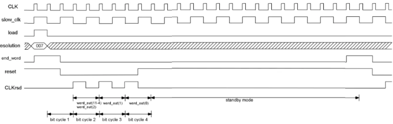
Figure 4.46: Block diagram of the digital component of the ADC... 100
Figure 4.47: Block diagram of the ADC ... 103
Figure 4.48: Timing diagram of the ADC for a 4-bit resolution... 105
Figure 4.49: Timing diagram of the ADC for a 12-bit resolution... 105
Figure 4.50: TSPC flip-flop ... 109
Figure 4.51: Layout of the FSM... 110
Figure 4.52: Signal generator of the strobe signals... 111
Figure 4.53: Timing diagram of control signals of the comparators... 111
Figure 4.54: Resolution controller ... 112
Figure 4.55: TSPC flip-flop with set and reset... 114
Figure 4.56: Circuit to generate the signal load ... 115
Figure 4.57: Layout of the resolution controller ... 115
Figure 4.58: Simulation results of the resolution controller... 116
Figure 4.59: Frequency divider ... 117
Figure 4.60: Timing Diagram for the frequency divider... 117
Figure 4.61: (a) RSD decoder cell ... 118
(b) Serial RSD to two’s complement decoder [9] ... 118
Figure 4.62: RSDreset signal generator ... 119
Figure 4.63: Clock generator of the RSD decoder ... 120
Figure 4.64: Input circuit of the RSD decoder ... 120
Figure 4.65: Timing diagram of the RSD decoder control signals ... 121
Figure 4.66: Exclusive-OR gate of the RSD decoder ... 122
Figure 4.67: Layout of the RSD decoder ... 122
Figure 4.68: Simulation results of the RSD decoder... 123
Figure 4.69: Layout of the digital component of the ADC [2] ... 124
Figure 4.70: (a) Circuit to generate the bias voltage Vbp (b) Circuit to generate the bias voltage Vb ... 126
Figure 4.72: Timing diagram for the control voltage generator of the bias
voltage generators ... 127
Figure 4.73: Common-centroid layout of the differential pair (M1, M2) ... 129
Figure 4.74: Test chip layout... 132
Figure 4.75: Pin diagram of the test chip ... 133
Figure 4.76: Minimum-size inverter ... 135
Figure 4.77: Generator of the test_out signal... 135
Figure 4.78: Layout of the test_out generator ... 136
Figure 4.79: Simulation results for the ring oscillator ... 137
Figure 4.80: Simulation results for the counter... 137
Figure 5.1 : Output word for the maximum input current ... 139
Figure 5.2 : Output word for the minimum input current ... 140
Figure 5.3 : Maximum power dissipation versus resolution ... 141
Figure 5.4 : Percentage of the maximum power dissipation versus resolution... 141
Figure 5.5 : Currents sourced by the current copiers of the ADC for the minimum input current... 146
Figure 5.6 : Currents sourced by the current copiers of the ADC for the maximum input current ... 148
List of Tables
Table 3.1 : Illustration of a 4-bit cyclic ADC ... 16
Table 3.2 : Illustration of a 4-bit RSD cyclic ADC... 23
Table 4.1 : Reference voltages for comparators... 50
Table 4.2 : Summary of the currents of the ADC ... 51
Table 4.3 : Parameters of the PMOS regulated-cascode current copier... 66
Table 4.4 : Parameters of the NMOS regulated-cascode current sources... 73
Table 4.5 : Parameters of the PMOS regulated-cascode current sources... 79
Table 4.6 : Transistor sizes of the comparator ... 84
Table 4.7 : Capacitor sizes for comparator reference voltages ... 87
Table 4.8 : The input voltage range and the corresponding 12-bit output word... 101
Table 4.9 : State transition table of the FSM... 107
Table 4.10: State encoding of the FSM... 108
Table 4.11: Operation for a 1-bit subtraction... 118
Chapter 1
Introduction
Analog-to-digital converters (ADCs) are a major component in digital
communications systems where signals transmitted over radio frequencies are received and subsequently converted to digital signals for digital signal processing. Digital signal processing is preferable to its analog counterpart since digital circuits are often more scalable, more reliable in noisy environments, faster, and cheaper to design than analog circuits. Additionally, most fabrication facilities are limited to cheaper CMOS digital processes where accurate analog components are unavailable. As a result, analog designs requiring accurate analog components are seldom used in modern communications systems.
Recently, portable wireless applications have made power dissipation a major concern in wireless applications. Applications such as cellular phones, pagers, and camcorders require small power dissipation to reduce the size and weight of batteries and to extend the lifetime of the battery. Also, increased complexity in signal processing for wireless video and wireless web in cellular phones has increased the necessity of low power dissipation.
An ADC used in wireless communications should meet the necessary
requirements for the worst-case channel condition. However, the worst-case scenario rarely occurs. As a consequence, a high-resolution and subsequently high-power ADC designed for the worst case is not required for most operating conditions. A solution to reduce the wasted power is to detect the current channel condition and change the resolution of the ADC dynamically such that an ADC with an appropriate resolution is used.
In this thesis, a low-power, variable-resolution ADC suitable for CMOS digital processes is investigated. Variable-resolution is investigated with the goal of reducing power dissipation when the resolution of the ADC is lowered. We have implemented an ADC whose resolution is dynamically adjustable according to the given channel
condition. The ADC has a maximum power dissipation of 6.35 mW for a 12-bit
resolution for a single-ended 3.3 V power supply voltage in a 0.35 µm technology. Also, when the resolution of our ADC is lower by two bits, our ADC has an average power savings of ten percent. Simulation results indicate our ADC achieves a bit rate of 1.7 MHz and has a signal-to-noise ratio (SNR) of 84 dB for the maximum input frequency of 16.7 kHz. The core size of our ADC is 1.26 mm2.
The organization of this thesis is as follows. Chapter 2 introduces important concepts of ADCs and reviews contemporary ADCs suitable for low-power applications. Feasibility of variable resolution is also investigated. Chapter 3 gives an overview of the proposed ADC architecture. The advantages of the proposed algorithm adopted by our ADC are also shown. Chapter 4 discusses the implementation of the algorithm and its components in detail. Chapter 5 presents the simulation results of our ADC, including accuracy, speed, and power dissipation for various resolutions. Chapter 6 concludes the thesis and presents future improvements.
Chapter 2
Background
2.1 Introduction
In this chapter, we review fundamentals of analog-to-digital converters (ADCs) and several types of ADC architectures. We also review low-power approaches to ADCs and contemporary high-performance ADC architectures. Finally, we investigate the feasibility of two ADC architectures for implementation of variable-resolution.
2.2 Fundamentals of Analog-to-Digital Converters
In this section we review the function of an ideal ADC and the major parameters of analog-to-digital converter (ADC) performance, which include the resolution, the effective number of bits, the integral nonlinearity error, the differential nonlinearity error, the conversion time, the sampling rate, and the power dissipation of ADCs.
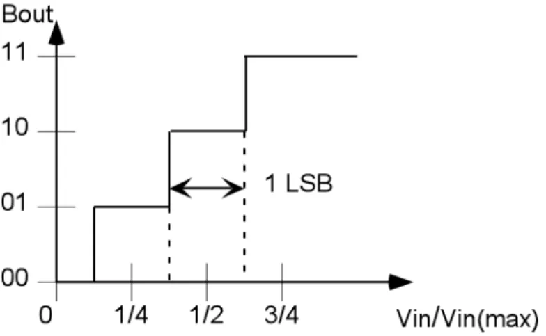
Figure 2.1 Transfer Characteristic of an Ideal 2-bit ADC
Figure 2.1 shows an ideal 2-bit ADC that produces a 2-bit digital word Bout for an analog input Vin. The input voltage has been normalized with respect its upper bound Vin(max). The bounds of the input voltage and the resolution N of an ADC determine the range of the input voltage that corresponds to the same output word. The range denoted as VLSB is given by N l u LSB L L V 2 − = ,
where N is the number of bits of the ADC, Lu is the upper bound of the input of the ADC, and Ll is the lower bound of the input of the ADC. Specifically, VLSB is the change of the input necessary to cause the least-significant bit of the output word to change. When VLSB is divided by the dynamic range (the difference of the upper bound and the lower bound) of the input, the resulting quantity is denoted as 1 LSB. As shown in the figure, 1 LSB is ¼ for a 2-bit ADC [12].
The transfer characteristic of an ideal ADC is defined mathematically by
(
Lu −Ll)
(
b12−1+b22−2 +b32−3 +L+bN2−N)
=Vin ±Vx,where Vx is the quantization error. Since a range of input voltage corresponds to a single output word, a quantization error is unavoidable. The quantization error for an ideal ADC is bound by the condition
LSB x LSB V V V 2 1 2 1 ≤ ≤ − .
Since VLSB is inversely proportional to 2N, the quantization error becomes smaller as the resolution grows larger, resulting in a more accurate digital representation of the input voltage [12].
The performance parameters used to characterize an ADC are the resolution, the effective number of bits, the integral nonlinearity (INL) error, the differential nonlinearity (DNL) error, the conversion time, the sampling rate, and power dissipation of the ADC. The resolution of an ADC is defined as the number of analog levels that correspond to unique binary words. Specifically, an N-bit ADC has 2N output words. If this definition is strictly followed, the resolution of a converter does not necessarily mean that the ADC is accurate to N bits. The accuracy of an ADC is determined by its effective number of bits, as will be shown next.
The signal-to-noise ratio (SNR) of an ADC gives the effective number of bits Ne. The SNR in decibels (dB) for an ADC with an effective number of bits, Ne, is given as
dB N
SNR =6.02 e+1.76
for a sinusoid that spans the entire input range of the ADC. The SNR is given by the ratio of the root-mean-square (rms) value of the input voltage and the rms value of the quantization noise [12]. The SNR maintains this value when the difference of the upper bound of the quantization noise and the lower bound of the quantization noise is VLSB (i.e. Vx(max)-Vx(min) = VLSB).
The effective number of bits of an ADC is the number of bits the ADC accurately computes. For example, assume that an ADC computes ten bits. However, an error causes the signal-to-noise ratio to be 50 dB. In such a case, the effective number of bits, Ne, is eight, as computed by the SNR equation. Thus, the effective number of bits can be less than or greater than the resolution of an ADC.
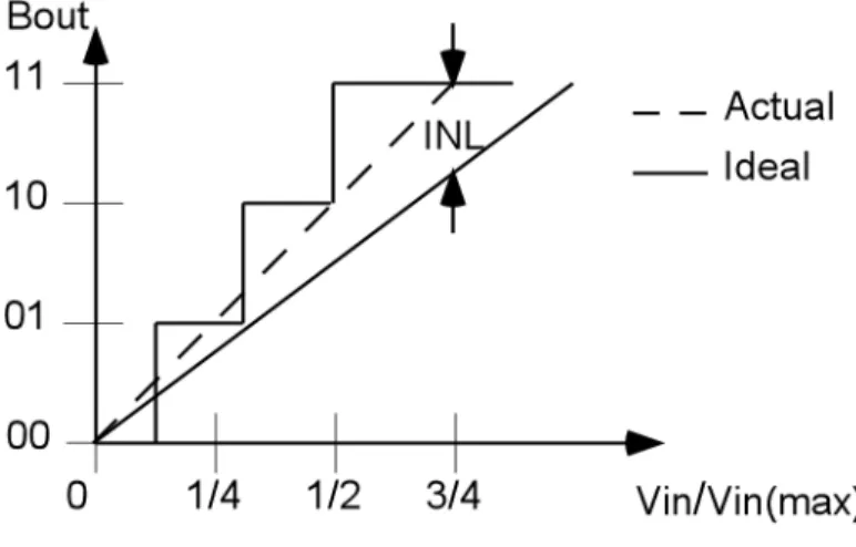
The INL error of an ADC is the deviation of the line through the endpoints of the transfer characteristic from the line through the endpoints of the ideal transfer
Figure 2.2 INL Error for a 2-bit ADC
The INL error is defined for each digital output word. Most literature reports the maximum INL error, which is an indication of the accuracy of the ADC. An ADC is guaranteed to be N-bit accurate if the INL error is less than ½ LSB [12].
The DNL error of an ADC is the deviation of the analog step sizes from 1 LSB. Figure 2.3 shows the DNL errors for output words "01" and "00" for a 2-bit ADC.
Figure 2.3 DNL Error for a 2-bit ADC
The DNL error of an ADC is also defined for each digital output word and is a measure of the accuracy of the ADC. When the DNL error of an ADC is less than 1 LSB, the ADC is guaranteed to be N-bit accurate [12].
The conversion time of an ADC is the amount of time taken to complete one digital word. The sampling rate is the speed that an ADC can continuously convert analog samples to digital words. The sampling rate is often the inverse of the conversion time, but some converters require latency between conversions [12]. If latency is
required between words, then the sampling rate includes the conversion time and the additional latency. The sampling rate is most often reported in samples per second (or Hertz) in literature.
The power dissipation of an ADC often reported is the amount of power required to complete a digital word. The power dissipation varies greatly with the conversion speed and the chosen ADC architecture. Also, power dissipation increases with increased accuracy since high-performance components, which typically have high power
dissipation, are necessary for accurate ADCs. Power dissipation also increases for architectures that utilize parallelism.
The performance parameters of an ADC mentioned in this section are greatly dependent on the type of architecture chosen to implement the ADC. Common types of ADC architectures and their limitations are reviewed in the next section.
2.3 Various Types of Analog-to-Digital Converter Architectures
In this section, we briefly review several types of analog-to-digital converters, the general operation, and the characteristics of each ADC presented. The types of ADCs discussed here are the flash, the successive-approximation, the cyclic, the pipelined, and the sigma-delta architectures.
Generally, the fastest analog-to-digital converters are flash converters. A flash ADC determines the digital output word by performing 2N parallel comparisons for an N-bit conversion. Since the hardware complexity of a flash ADC increases exponentially with resolution, power dissipation increases accordingly. Thus, flash ADCs are often limited to four to six bits. Interpolating or folding techniques use analog pre-processing blocks to reduce the amount of parallel comparisons, allowing greater resolution for less hardware complexity without decreasing the conversion rate of the ADC [12]. However, the analog pre-processing blocks grow increasingly complex as the number of parallel comparisons decreases. As a result, high-resolution interpolating and folding ADCs are seldom implemented.
digital word is completed in N conversion cycles for an N-bit cyclic (or an N-bit successive-approximation) ADC. Due to the iterative approach, these ADCs utilize a small amount of hardware when compared with other types of converters. The reduction in circuit complexity is gained at the cost of conversion speed since N conversion cycles are required to complete the conversion. To maintain a constant conversion rate, cyclic and successive-approximation ADCs must operate with linearly increasing speed as the resolution increases. Cyclic and successive-approximation converters are one of the most popular approaches for analog-to-digital converter implementations due to the reasonably fast conversion speed and moderate circuit complexity [12].
A pipelined analog-to-digital converter is broken into stages of small-resolution (typically 1.5 bits) ADCs where each stage computes one bit per conversion cycle. When the first stage of a pipeline finishes computing the most-significant bit of the digital output for the current analog sample, the next stage starts to compute the next most-significant bit for the same analog sample. At the same time the first stage computes the most-significant bit for the next analog sample. In this manner, no stage of the pipeline is ever idle, and the analog-to-digital converter is continually working on new data in each conversion cycle. Thus, a pipelined analog-to-digital converter has a throughput
comparable to a flash converter [12]. Due to the parallel architecture, power dissipation grows with increased resolution.
The ADC architectures discussed above are called rate ADCs. Nyquist-rate ADCs produce one N-bit digital output for each analog input at the Nyquist Nyquist-rate. A different approach is called an oversampling ADC, which utilizes oversampling
techniques. An oversampling ADC includes a sigma-delta modulator that produces a low-resolution digital output (typically one to two bits) for every analog sample at a much faster speed than the Nyquist rate (typically 20 to 512 times the Nyquist rate). The quantization noise of the digital output of the modulator is digitally filtered to produce a higher-resolution digital output. As the oversampling rate increases, the accuracy of the ADC increases. Oversampling techniques provide a trade-off between analog and digital circuit complexity [12]. This trade-off is advantageous in digital processes where
sigma-delta converters use a high oversampling rate, these converters generally have moderate conversion times.
2.4 Low-Power Analog-to-Digital Converter Design Approaches
Since low-power ADC designs are necessary for many applications, such as portable devices, most types of ADC architectures have been designed with low power dissipation as an objective. Most approaches for low-power analog designs are specific to the application at hand. Some general techniques for lowering power dissipation have been used in many ADC designs and are described in this section.
A technique often employed in low-power analog designs is lowering the supply voltage. Since power dissipation is quadratically related to the supply voltage, this approach reduces power dissipation. However, MOSFETs are often cascaded in analog designs. Since cascaded devices require a larger voltage drop across the cascade, lowering the supply voltage may not be feasible.
Many classic analog designs use resistors in their implementation. However, resistors have large quiescent power dissipation. As a result, resistive circuits are not good candidates for low-power designs. In architectures that employ resistor ratios, resistors can be replaced with capacitors. Since capacitors do not dissipate steady-state power, this technique reduces power dissipation.
A common component for ADCs is a comparator that produces the digital output of the ADC. For high-accuracy ADCs, high-gain comparators that use
offset-cancellation techniques are often required. Such comparators have large power dissipation. One approach to reduce the necessary comparator power dissipation is to reduce or eliminate the need for high-gain components with offset-cancellation. This objective is accomplished by implementing digital error correction or by adopting algorithms immune to offsets. This approach is important for pipelined or flash converters since parallel comparators are used in these architectures. We employ this approach in our ADC design.
2.5 Review of Contemporary Analog-to-Digital Converters
In this section, we review state-of-the-art analog-to-digital converters. Since we wish to implement our analog-to-digital converter in a standard digital CMOS process, we will not consider ADC architectures implemented in other technologies, such as BiCMOS or gallium-arsenide. Also, in order to make a fair comparison between architectures, we propose the following figure of merit (FOM)
P
R
S
FOM
=
*
,where S is the conversion rate or speed of the ADC in kiloHertz (kHz), R is the resolution of the ADC in bits, and P is the power dissipation in milliWatts (mW). A larger FOM implies a more efficient ADC design. The figure of merit does not take into account the power supply voltage or the CMOS technology used, but it is helpful for a general comparison.
Low-power ADCs designed in CMOS technologies were investigated extensively in the past decade [1], [3], [4], [5], [7], [9], [11], [13], [15], [19], [20], [21], [22], [23], [24], [25], [26], [29], [30], [31], [32]. Venes and Plassche reported an 8-bit, folding analog-to-digital converter with a sampling frequency of 80 MHz and a power dissipation of 80 mW. Folding techniques are used to reduce the number of comparators in a flash converter. Venes and Plassche partitioned their ADC into a 3-bit coarse ADC and a 5-bit fine ADC using a folding rate of 32 as a tradeoff between the number of required
comparators and the complexity of the analog preprocessing block. The reported SNR of the ADC is 44 dB or 7.5 effective bits of resolution. The reported maximum INL of the ADC is 0.8 LSB, and the maximum DNL is 0.45 LSB [29]. Venes and Plassche's architecture has a FOM value of 8000.
Baird and Fiez developed a 14-bit, 500 kHz, sigma-delta ADC with a power dissipation of 58 mW. Baird and Fiez reduced the oversampling rate by utilizing a 4-bit sigma-delta modulator in their converter. Since the accuracy of the digital output is greater than the typical 1-bit resolution, the oversampling rate and power dissipation were
reduced. This architecture has a SNR of 86 dB or 14.3 effective bits [3]. Their architecture has a FOM value of 120.
Cho and Gray reported a 10-bit, 20 MHz, 35 mW, pipelined ADC. Cho and Gray applied several techniques to reduce the power dissipation of the pipelined ADC. They lowered the supply voltage from 5 V to 3.3 V, and capacitors were reduced to the minimal size necessary to overcome thermal noise. However, the reduction in capacitor sizes did require some additional circuitry. Digital-error correction was implemented to reduce the comparator requirements. The components in the latter stages of the pipeline were scaled down with respect to speed and accuracy since requirements of the latter stages of the pipeline are less rigorous than the first stages of the pipeline. The reported SNR is 62 dB or 10.3 effective bits. The reported maximum INL is 0.6 LSB, and the maximum DNL is 0.5 LSB [7]. Cho and Gray’s ADC has a FOM value of 5714.
A 12-bit, 0.83 MHz, 2 mW, switched-current, redundant signed-digit cyclic converter was reported by Wang and Wey. Their ADC is based on the redundant signed-digit (RSD) cyclic algorithm. The RSD cyclic algorithm is immune to loop and
comparator offsets, consequently reducing the comparator requirements of the ADC. Wang and Wey also lowered the power supply voltage from 5 V to 3.3 V. Wang and Wey reported a SNR of 74 dB or 12.3 effective bits, an INL of 0.45 LSB, and a DNL of 0.6 LSB [30]. Wang and Wey's ADC has a FOM value of 5000.
The figure of merits for the converters discussed above indicate that the flash converter proposed by Venes and Plassche is the best approach. However, low-power, high-resolution flash converters are not feasible due to the high degree of parallelism and large power dissipation. Thus, the best candidates for a high-resolution, low-power analog-to-digital converter are pipelined and cyclic converters. Since we wish to implement a variable-resolution analog-to-digital converter, we will discuss the
feasibility of a variable-resolution approach for the pipelined ADC proposed by Cho and Gray and the cyclic ADC proposed by Wang and Wey in the following section.
2.6 Feasibility of Variable-Resolution Analog-to-Digital Converters
While each type of converter mentioned in Section 2.3 has its own merit for some applications, we are investigating a low-power analog-to-digital converter with variable resolution in this thesis. Good candidates for a variable-resolution ADC are the pipelined and cyclic implementations described in Section 2.5.
The 10-bit, pipelined ADC presented by Cho and Gray is a switched-capacitor approach [7]. Specifically, each of the ten stages of the pipeline consists of a high-speed, high-gain op-amp and capacitors. To implement variable resolution, the most obvious approach would be to dynamically disable the latter stages of the pipeline. However, operational amplifiers dissipate a large amount of steady-state power even when they are not performing a useful function. Consequently, disabling the latter stages of the pipeline would not save a large amount of power. While Cho and Gray's implementation exhibits low-power dissipation, the switched-capacitor implementation does not easily lend itself to a variable-resolution approach.
The 12-bit, redundant signed-digit cyclic ADC presented by Wang and Wey is based on a switched-current approach [30]. In Wang and Wey's architecture, the main components of the ADC are four MOSFET-capacitor pairs, four current sources, and one moderate-gain op-amp. An approach to variable resolution for a cyclic converter is limiting the number of conversion cycles for a lower-resolution conversion. Opening all the switches in the architecture effectively disables the switched-current converter. In Wang and Wey's architecture, no steady-state power is dissipated when its switches are open with the exception of the power dissipation of the moderate-gain op-amp. As a result, steady-state power would be small when the converter is disabled. Furthermore, the redundant signed-digit cyclic algorithm allows for low-power comparators that do not dissipate steady-state power. Also, since their architecture is based on switched-current techniques, it is appropriate for digital processes where precision analog components are not required. This advantage will be discussed further in the next chapter. Thus, Wang and Wey's cyclic converter is a good approach for a variable-resolution ADC, which aims to reduce power dissipation.
In this chapter we showed that a switched-current, redundant signed-digit cyclic ADC is a good approach for a variable-resolution, low-power, analog-to-digital
converter. In the following chapter, we discuss the major components of the ADC in detail.
Chapter 3
Features of the Analog-to-Digital Converter Architecture
3.1 Introduction
In this chapter, we provide an overview of switched-current, redundant signed-digit (RSD) cyclic analog-to-signed-digital converters (ADCs) related to the implementation of our ADC. First, we review cyclic analog-to-digital converters and then briefly describe the RSD cyclic algorithm and its advantages. We also describe an appropriate
comparator for our ADC and then the common architectures of current copiers. Finally, we present an approach for achieving variable resolution, which is implemented in our ADC to reduce power dissipation.
3.2 Conventional Cyclic Analog-to-Digital Converters
A conventional cyclic ADC applies an iterative algorithm to determine the digital output of the ADC, where the input of the ADC can be a current or a voltage.
Specifically, a cyclic ADC calculates one bit per conversion cycle beginning with the most significant bit (MSB). Unlike flash or pipelined ADCs, parallel hardware is not required for cyclic ADCs to result in a hardware efficient implementation. However, hardware efficiency is gained at the cost of conversion speed since cyclic ADCs require N conversion cycles for an N-bit conversion.
3.2.1 Conventional cyclic conversion algorithm
The cyclic algorithm is based on the conventional restoring division principle [9]. A flow-graph describing the cyclic conversion algorithm for an unsigned, N-bit, current-mode, cyclic ADC is shown in Figure 3.1.
Ires Iin i N-1 Ires 2Ires
>Iref
bi 0 bi 1
Ires Ires-Iref
i i-1 i 0 Stop Yes No No Yes Ires Iin ≤
The residue current Ires in Figure 3.1 is initially the sampled input current Iin, and the loop variable i is set to the resolution N of the ADC. The initial residue current Ires is then multiplied by two and compared to the reference current Iref. The reference current is set to the dynamic range of the ADC, which is the difference of the maximum input current and the minimum input current (i.e. [Imax-Imin]). If 2Ires is greater than the reference current, the current bit bi is set to a digital ‘1’, and the residue current is reduced by Iref. Otherwise, the current bit is set to a digital ‘0’, and the residue current remains the same. The loop variable is decremented by one, and the process repeats N times. The loop transfer characteristic can be expressed as
≤ > = ≤ > = − ref res ref res i ref res res ref res ref res res I I if I I if b I I if I I I if I I I 2 0 2 1 2 2 2 2 * ,
where Ires* is the updated residue current used in the next conversion cycle and Ires is the
initial residue current.
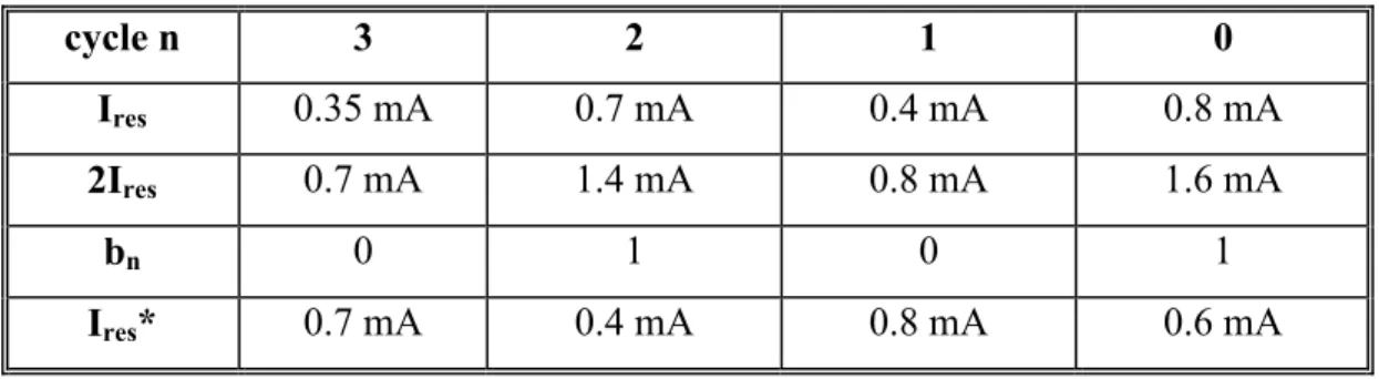
The conversion process of a cyclic ADC is illustrated for a 4-bit ADC, where the dynamic range of the ADC extends from 0 mA to 1 mA and the reference current is 1 mA. The residue current and the bit generated for each conversion cycle are given in Table 3.1 for a sampled input current of 0.35 mA.
Table 3.1 Illustration of a 4-bit Cyclic ADC
cycle n 3 2 1 0
Ires 0.35 mA 0.7 mA 0.4 mA 0.8 mA
2Ires 0.7 mA 1.4 mA 0.8 mA 1.6 mA
bn 0 1 0 1
3.2.2 Offset requirements
A limitation of a conventional cyclic ADC is its offset requirements. A Robertson diagram represents the loop transfer function of a cyclic ADC and is useful for
illustrating the offset limitations. The horizontal axis of the Robertson diagram shown in Figure 3.2 is twice the initial residue current, which is the quantity used for comparison with the reference current in the current conversion cycle. The vertical axis is the
updated residue current, Ires*.
Figure 3.2 Robertson Diagram of a Conventional Cyclic ADC [9]
The region of convergence shown in Figure 3.2 is the range of the initial residue current and the updated residue current for which the cyclic algorithm converges. If the
updated reside current, Ires*, exceeds the bounds of the region of convergence, the cyclic
algorithm diverges since the residue current grows further from the bounds of the region of convergence with each iteration. Thus, after a cyclic ADC leaves the region of convergence, the ADC is effectively overloaded. Figure 3.2 shows that the region of
convergence of a conventional cyclic ADC is [0, Iref] for Ires* and [0, 2Iref] for 2Ires. The
requirement to stay in the region of convergence determines the offset limitations of a cyclic ADC.
In Figure 3.2, the line designated as b=1 is the one defined by Ires* = 2Ires-Iref in
the interval [Iref, 2Iref], and the line designated as b=0 is the one defined by Ires* = 2Ires in
the interval [0, Iref]. The diagram shows that the current bit is set to ‘0’ if 2Ires is less than
Iref, and Ires* = 2Ires; otherwise, the current bit is set to ‘1’, and Ires * = 2Ires-Iref.
Figure 3.2 indicates the only appropriate comparison level is Iref. If the actual
comparison level of a conventional cyclic ADC is I instead of Iˆref ref due to an offset, the
ADC leaves its region of convergence under certain conditions, as demonstrated next. If ef
r ˆ
I is greater than Iref, the residue current used in the next conversion cycle, Ires*, exceeds
Iref for I > 2Iˆref res > Iref. When 2Ires is less than I , the reference current is not subtracted ˆref
from 2Ires. However, 2Ires exceeds Iref. Ires* then becomes 2Ires, which is greater than Iref.
Consequently, the ADC leaves the region of convergence.
If the actual comparison level is greater than Iref and the residue current is less
than Iref for a particular conversion cycle, the ADC does not leave the region of
convergence. However, the ADC leaves the region of convergence when I > 2Iˆref res > Iref.
Thus, under this condition, the ADC only converts analog inputs that map to the output word consisting of all zeros (i.e. "00...0") correctly.
Furthermore, if I is less than Iˆref ref, the residue current used in the next conversion
cycle is less than zero for Iref > 2Ires > I . When 2Iˆref res is greater than I , the reference ˆref
current is subtracted from 2Ires, which is less than Iref. The updated residue current, Ires*,
becomes 2Ires-Iref, which is less than zero. Consequently, the ADC leaves the region of
convergence.
If the actual comparison level is less than Iref and the residue current is greater
than Iref for a particular conversion cycle, the ADC does not leave the region of
convergence. However, the ADC leaves the region of convergence when Iref > 2Ires >
ef r ˆ
I . However, the ADC only converts analog inputs that map to the output word "11...1" correctly.
The Robertson diagram of the cyclic ADC with a positive comparator offset ∆c
(i.e. I > Iˆref ref) is shown in Figure 3.3. Figure 3.3 shows that if 2Ires is in the range [Iref,
Figure 3.3 Robertson Diagram of a Conventional Cyclic ADC with a Comparator
Offset +∆c [9]
The actual comparison level, I , of a conventional cyclic ADC must be within ˆref
½ ILSB of Iref to maintain an N-bit accuracy. (Note ILSB is defined as (Imax – Imin)/2N.) For
any loop offset less than or equal to ½ ILSB, the difference of the bounds of the
quantization error remains less than ILSB; thus, the digital output of the ADC has N
effective bits as given by the SNR equation. However, if a loop offset is greater than ½
ILSB, a conventional cyclic ADC leaves its region of convergence, resulting in less than
N-bit accuracy. Since constant loop offsets are often present in the hardware
implementation of an ADC and cyclic ADCs are sensitive to offsets, a high-resolution cyclic ADC needs offset-cancellation techniques. Note that the offset may be due to a comparator offset or a constant offset elsewhere in the loop.
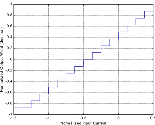
The ADC transfer characteristic for a signed, 4-bit ADC with a constant loop
-1 -0.8 -0.6 -0.4 -0.2 0 0.2 0.4 0.6 0.8 1 -1 -0.8 -0.6 -0.4 -0.2 0 0.2 0.4 0.6 0.8 1
Norm alized Input Current
Nor m al iz ed O u tp ut W o rd ( dec im al )
Figure 3.4 Transfer Characteristic of a Conventional Cyclic ADC with a Loop Offset of
+ILSB
The horizontal axis of Figure 3.4 is the normalized input current, which ranges from -1 to 1, and the vertical axis is the normalized output word in decimal, which is found by
dividing the decimal equivalent of the output by 2N. Figure 3.4 shows that the analog
step sizes are neither uniform nor 1 ILSB in step size when an offset of ILSB is present. In
fact, the difference of the bounds of the quantization error exceeds ILSB, giving a SNR
less than that required for eight effective bits. Thus, the ADC does not have 8-bit accuracy. Figure 3.3 and Figure 3.4 show a loop offset due to a comparator offset or a constant loop offset reduces the accuracy of a conventional cyclic ADC.
3.3 Redundant Signed-Digit Cyclic Analog-to-Digital Converters
In this section, we describe redundant signed-digit (RSD) cyclic ADCs and their advantages over conventional cyclic ADCs. An ADC based on the RSD algorithm is a
cyclic ADC with a ternary alphabet {-1, 0, 1} rather than a binary alphabet {0, 1}. However, the actual representation of the output bits of a RSD cyclic ADC is binary by necessity, and the binary representation is specific to the underlying hardware
implementation (to be discussed in Chapter 4). Like a conventional cyclic ADC, a RSD cyclic ADC calculates one bit per conversion cycle beginning with the most significant bit. However, use of a ternary alphabet for a RSD cyclic ADC makes it tolerant of loop offsets and comparator inaccuracy.
3.3.1 RSD cyclic conversion algorithm
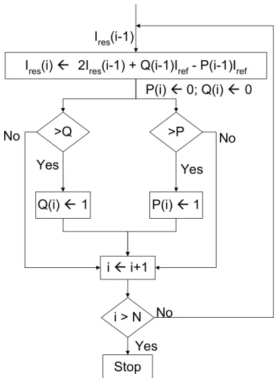
The RSD cyclic conversion algorithm is based on the Sweeney-Robertson-Tocher division principle [9]. A flow-graph illustrating the signed RSD cyclic conversion
>2P Ires Iin i N-1 Ires 2Ires <2Q bi -1 bi 1
Ires Ires - Iref
i i-1 i 0 Stop No No Yes Ires Iin ≤
Ires Ires+ Iref
bi 0
Yes Yes
No
Figure 3.5 Flow Graph for the RSD Cyclic Conversion Algorithm [9]
As shown in Figure 3.5, the residue current Ires is initially the sampled input current, and
the loop variable i is set to the resolution N of the ADC. The residue current is then
multiplied by two, and two parallel comparisons are performed between 2Ires and the two
constant comparison levels 2Q and 2P. 2Q is in the range of [-Iref, 0], and 2P is in the
range of [0, Iref]. The reference current, Iref, is the difference of the maximum input
current and the minimum input current divided by two (i.e. (I max – Imin)/2). If 2Ires is less
greater than 2P, the current bit is ‘1’, and the reference current is subtracted from 2Ires. If
Ires is greater than 2Q but less than 2P, then the residue current remains the same, and the
current bit is ‘0’. The loop variable is decremented by one, and the process repeats N times. The loop transfer characteristic can be expressed by
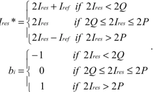
> ≤ ≤ < − = > − ≤ ≤ < + = P I if P I Q if Q I if b P I if I I P I Q if I Q I if I I I res res res i res ref res res res res ref res res 2 2 1 2 2 2 0 2 2 1 2 2 2 2 2 2 2 2 2 2 * .
The conversion process of a RSD cyclic ADC is illustrated for a 4-bit ADC, where the dynamic range of the ADC extends from -1 mA to 1 mA and the reference current is 1 mA, which is the dynamic range of the ADC divided by two. The
comparison levels 2P and 2Q are chosen to be 0.5 mA and –0.5 mA, respectively. The residue current and the bit generated for each conversion cycle are given in Table 3.2 for the sampled input current of 0.35 mA.
Table 3.2 Illustration of a 4-bit RSD Cyclic ADC
cycle n 3 2 1 0 Ires 0.35 mA -0.3 mA 0.4 mA -0.2 mA 2Ires 0.7 mA -0.6 mA 0.8 mA -0.4 mA bn 1 -1 1 0 Ires* -0.3 mA 0.4 mA -0.2 mA -0.4 mA
3.3.2 Offset requirements
While a RSD cyclic ADC is similar to a conventional cyclic ADC, it does not have the same offset requirements under certain conditions. The requirements on the ranges of 2Q and 2P are examined to identify the conditions. As mentioned previously,
2Q should be in the range [-Iref, 0], and 2P is should be in the range [0, Iref]. The range
requirements of 2Q and 2P are illustrated with the three Robertson diagrams in Figure 3.6.
Figure 3.6 (b) Robertson Diagram of a RSD Cyclic ADC for 2P = -2Q = 0
Figure 3.6 (c) Robertson Diagram of a RSD Cyclic ADC for 2P = -2Q = Iref/2 [9]
The region of convergence shown in the three diagrams is [-2Iref, 2Iref] for 2Ires
shows the case of 2P = Iref and 2Q = -Iref. It will be shown that Ires remains in the region
of convergence if 2P = -2Q = Iref. Ires also remains in the region of convergence for the
case shown in Figure 3.6 (b), where 2P = 2Q = 0. Figure 3.6 (c) shows the general case
where 0 < 2P < Iref and –Iref < 2Q < 0. We show that Ires remains within the region of
convergence for 0 ≤ 2P ≤ Iref and –Iref ≤2Q ≤ 0 next.
Suppose that 2P > 2Ires > Iref > 2Q. As 2Ires is less than 2P and greater than 2Q,
Ires* is 2Ires. However, 2Ires exceeds Iref; thus, Ires* is greater than Iref, which causes the
ADC to leave the region of convergence. Now, suppose that 0 > 2Ires > 2P > 2Q. As 2Ires
is greater than 2P, Ires* = 2Ires-Iref. However, 2Ires is less than zero; thus, Ires* is less than
-Iref. Consequently, the ADC leaves the region of convergence. Thus, 2P should be in the
range [0, Iref]. Similar arguments can be made for the range requirement of 2Q.
If the comparison levels 2P and 2Q are set to the limits of their required ranges
(i.e. 2P = -2Q = Iref or 2P = 2Q = 0), the comparator offset of a RSD cyclic converter
cannot exceed ½ ILSB. In this case, the tolerable offset is the same as a conventional
cyclic ADC. However, if 2P and 2Q are within their required ranges, the comparator
offset can exceed ½ ILSB. The Robertson diagram of Figure 3.6 (c) illustrates such a case.
Setting 2P and 2Q to Iref/2 and -Iref/2, respectively, gives the maximum
comparison level tolerance Iref/2 [9]. Given that 2P is Iref/2 and Ires = 0, suppose the
comparator makes the wrong decision by setting bi = ‘1’ (rather than bi = ‘0’) due to a
comparator offset. The updated residue current is Ires* = 2Ires-Iref = -Iref, which is in the
region of convergence of the ADC. Likewise, given that 2P is Iref/2 and Ires = Iref/2,
suppose that the comparator makes the wrong decision by setting bi = ‘0’ (rather than bi =
‘1’) due to a comparator offset. The updated residue current is then Ires* = 2Ires = Iref,
which is in the region of convergence. The Robertson diagram for a RSD cyclic ADC
resulting from a comparator offset ∆c of Iref/2 with 2P = -2Q = Iref/2 is shown in Figure
3.7. The figure shows that a RSD cyclic ADC remains in its region of convergence for this comparator offset.
Figure 3.7 Robertson Diagram of a RSD Cyclic ADC with a Comparator Offset +Iref/2
In the above, we showed that setting 2P = -2Q = Iref/2 provides the maximum
tolerance for comparator offsets. Setting 2P = -2Q = Iref/2 also provides the maximum
tolerance for constant loop offsets. If a constant loop offset is added after the
multiplication by two, an RSD cyclic ADC can withstand loop offsets less than or equal
to Iref/2 for 2P = -2Q = Iref/2. In this case, the quantization error of an N-bit RSD cyclic
converter is less than 1/2 ILSB, assuming no other errors are present. As a result,
offset-cancellation techniques are rarely required for RSD cyclic ADCs.
Figure 3.8 shows the transfer characteristic of a RSD cyclic ADC with a loop
-1.5 -1 -0.5 0 0.5 -1 -0.8 -0.6 -0.4 -0.2 0 0.2 0.4 0.6 0.8 1
Norm alized Input Current
Nor m al iz ed O u tp ut W o rd ( dec im al )
Figure 3.8 Transfer Characteristic of the RSD Cyclic ADC with a Loop Offset of +Iref/2
Figure 3.8 shows the input dynamic range experiences a vertical shift of Iref/2, which is
the loop offset. However, the linearity of the RSD cyclic ADC is not affected by the loop
offset. Thus, setting 2P = -2Q = Iref/2 is the optimum choice for 2P and 2Q to provide
tolerance for any offsets present in a RSD cyclic ADC.
While an N-bit conventional cyclic ADC requires a loop offset less than or equal
to ½ ILSB for N-bit accuracy, an N-bit RSD cyclic ADC maintains N-bit accuracy for
offsets less than or equal to Iref/2 for 2P = -2Q = Iref/2. Since ILSB is proportional to 1/2N,
ILSB is much smaller than Iref/2 for high-resolution converters. Thus, RSD cyclic
3.3.3 Advantages of the RSD cyclic conversion algorithm
The RSD cyclic conversion algorithm is superior to the conventional cyclic conversion algorithm with respect to loop offsets and required comparator accuracy. A conventional cyclic ADC with high resolution requires a precise comparison against the reference current in order to remain within its region of convergence. A precise
comparison demands high gain components with offset cancellation. In contrast, the RSD algorithm allows relatively large comparator offsets.
Another advantage of the RSD cyclic conversion algorithm is its immunity to loop offset errors. As mentioned in Section 3.2, the loop offset of a conventional ADC
does not exceed ½ ILSB for an ADC with N-bit accuracy. As a result, a high-accuracy
cyclic ADC frequently requires offset-cancellation techniques since constant loop offsets are often present in the hardware implementation of an ADC and cyclic ADCs are
sensitive to offsets. However, as long as the loop offset does not exceed the tolerance set by the comparison levels 2P and 2Q, a RSD cyclic ADC remains in its convergence region. If an offset is present in a RSD cyclic ADC, the input dynamic range simply experiences a vertical shift.
While a RSD cyclic ADC is superior to a conventional cyclic ADC with respect to offsets, the cost of superiority is an additional comparator. However, comparators of a RSD cyclic ADC need not be accurate due to the comparator-offset insensitivity of a RSD cyclic ADC. A simple comparator suitable for a RSD cyclic ADC is explored in the next section.
3.4 Comparator
In this research, the RSD cyclic conversion algorithm is employed due to its superiority over the conventional cyclic conversion algorithm. The RSD cyclic
conversion algorithm greatly relieves the constraints on the comparators used in an ADC
-Iref/2, respectively, the required offset of the comparators of a RSD cyclic ADC is Iref/2. Thus, a simple comparator architecture can be used for RSD cyclic ADCs.
A comparator often used in ADCs based on the RSD algorithm consists of two strobed and cross-coupled inverters. The circuit diagram for such a comparator is given in Figure 3.9.
Figure 3.9 Circuit Diagram of a Strobed, Cross-Coupled Inverter Comparator [9]
The transistor pair M1 and M2 form one inverter, and the transistor pair M3 and
M4 form another inverter. The inverters are cross-coupled, as shown in the figure. Vin+
and Vin- are the input voltages, where one input voltage is chosen to be the comparison level for the comparator. The outputs of the two inverters, Vout+ and Vout-, are the outputs of the comparator.
When strobe is low, Vin+ and Vin- charge the parasitic gate capacitances of the inverters. However, no path exists from the supply rails (i.e. Vdd and ground) since the
transistors M7 and M8 are off. Consequently, Vout- follows Vin-, and Vout+ follows
Vin+. When the strobe signal transitions from low to high, M5 and M6 are turned off and
the input voltages are sampled at the gates of the inverters. When the strobe signal is high, the circuit of Figure 3.9 simplifies to two coupled inverters. The
cross-coupled inverters amplify the difference between the two input voltages, forcing the output voltages to the appropriate digital values for the given comparison level and input voltage. For example, suppose that the comparison level is chosen to be Vin- = Vdd/2 = 1.65 V and the input voltage is Vin+ = 0.5 V. Vout+ settles to ground, and Vout- settles to Vdd. The output voltages indicate that Vin+ is less than Vin-.
Since a strobed, cross-coupled inverter comparator consists of fully
complementary logic, it consumes a negligible amount of steady-state power. The comparator dissipates power only during the period when the inverters are amplifying the difference between the input voltages. Thus, a strobed, cross-coupled inverter
comparator is suited to low-power applications. 3.5 Current Copiers
The analog-to-digital converter that we investigated in this thesis employs a switched-current architecture. In switched-current architectures, all the variables of interest are currents rather than voltages. A major building block of switched-current architectures is a current copier. A current copier acts as a current memory, which stores current. We review several current copiers in this section. The descriptions of the current copiers are given in [27].
3.5.1 Simple current copier
A simple current copier consists of a single transistor and a capacitor. The circuit diagram is shown in Figure 3.10.
Figure 3.10 A Simple Current Copier [28]
During phase φ1, the drain and gate of the transistor are connected, and the signal
current i plus the bias current J is sourced to the copier cell. The total current, J+i, initially charges the gate capacitance C. Eventually, the gate capacitance is charged to
the voltage that causes the memory transistor Tm to conduct current J+i. At this point, the
current copier cell has memorized the signal current i.
During phase φ2, the switch connecting the gate and drain of the transistor is
opened, disconnecting the memory transistor from the input current. Also, the drain of the memory transistor is connected to the output of the current copier cell. Since the gate capacitance is charged to the voltage that causes the transistor to have a drain current of J+i, the output current is –i, assuming that the memory transistor operates in the
saturation region. Hence, the current copier is acting as a current source with current value i [28]. Note that if the memory transistor is not in the saturation region, the drain current is dependent on the drain voltage as well as the gate voltage of the transistor, greatly diminishing the accuracy of the current copier.
The current copier is suitable for digital processes since the value of the capacitor of the regulated-cascode current copier is not critical. Specifically, since the capacitor of the current copier is only used to store a voltage, the value of the stored current is not dependent on the value of the capacitor. Thus, the current copier does not require precise analog components, which are not available in digital processes.
While this architecture is simple, it is not accurate. The accuracy of the simple current copier is limited by two main factors. First, the current memorized during phase
φ1 is not equal to the current sourced in phase φ2 due to the secondary channel-length
modulation effect. The channel-length modulation effect is the phenomenon where the
effective channel length of a MOSFET is reduced as the drain-source voltage Vds
increases, producing higher drain currents for higher drain-source voltages. The
channel-length modulation effect results in a drain-source conductance gds that is given by
ds ds
I
g
=
λ
,where λ is the channel-length modulation coefficient and Ids is the drain-source current
of the memory transistor. Since the drain current of a transistor is dependent on its drain and gate voltage, the current copier does not source an output current of -i if the
drain-source voltage differs from phase φ1 to phase φ2.
Secondly, when the switch at the gate of the memory transistor is open during
phase φ2, changes in the drain voltage cause current to flow from the gate-drain overlap
capacitance Cdg into the memory capacitance C. This current causes the gate-source
voltage of the memory transistor to change during phase φ2, producing an error in the
stored current.
Channel-length modulation and the change in the gate-source voltage of the
memory transistor due to Cdg produce an error current δIds, which results from the change
in the drain-source voltage δVds of the memory transistor. The error current is given by
+
+
=
m dg dg ds ds dsg
C
C
C
g
V
I
δ
δ
,where gm is the small-signal input conductance of the memory transistor. The memory
transistor can be modeled as an ideal transistor with an output conductance go connected
from its drain to its source, which is defined by
m dg dg ds o
g
C
C
C
g
g
+
+
=
.Consider two identical, cascaded current copiers as shown in Figure 3.11, where one current copier is sourcing current to a second current copier.
Figure 3.11 Two Identical, Cascaded Simple Current Copiers [27]
Each current copier is modeled as an ideal transistor with an output conductance go.
When the first current copier is sourcing its stored current to the second current copier, the z-transform of the transfer function H(z) obtained as
m o i m o o
g
g
z
H
g
g
z
z
i
z
i
z
H
2
1
)
(
2
1
)
(
)
(
)
(
2 1+
=
+
−
=
=
,where io(z) is the output current of the first current copier in the z domain, i(z) is the input
current of the second current copier in the z domain, and Hi(z) = -z -1/2 is the ideal transfer
function of the two cascaded current copiers. For physical frequencies z=ejωT, the
transfer function H(z) becomes
m o T j i T j
g
g
e
H
e
H
2
1
)
(
)
(
+
=
ω ω ,where T is the period of the clock signals φ1 and φ2. An approximation to relate the
actual frequency response to the ideal frequency response for small errors is given by
)
(
)
(
1
)
(
)
(
ω
θ
ω
ω ωj
m
e
H
e
H
T j i T j−
−
=
,where m(ω) is the magnitude difference from the ideal frequency response, and θ(ω) is the phase difference from the ideal frequency response. The magnitude error and phase error for the simple current copier are given by
0 ) ( , 2 ) ( = = − = ω θ ε ω G m o g g m ,
where the transmission error εG is the magnitude difference between the current
memorized during phase φ1 and the current sourced by the memory transistor during
phase φ2. The transmission error is given by
+ + − = C C C g g dg dg m ds G 2 ε .
Thus, to decrease the transmission error, the output conductance of the current copier cell must be decreased, and/or the small-signal conductance must be increased. Long-channel
devices reduce the output conductance, go, but larger devices result in reduced bandwidth
due to larger parasitic capacitances [27]. Several alternative architectures have been proposed to stabilize the drain voltage of the current copier cell. Among these are the op-amp active current copier and the regulated-cascode current copier, which are described in the next section.
3.5.2 Op-amp active current copier
An op-amp active current copier consists of a simple current copier with a feedback amplifier. The circuit diagram of an op-amp active current copier is given in Figure 3.12.
Figure 3.12 An Op-Amp Active Current Copier [28]
During phase φ1, the drain of the memory transistor Tm is connected to one of the
differential inputs of the op-amp, the bias current J, and the input signal current i. The gate of the transistor is connected to the single-ended output of the op-amp. Initially, the input current i acts to disturb the voltage at the input terminal of the op-amp.
Consequently, the op-amp sources a current to the gate capacitance of the memory transistor. This feedback loop reaches equilibrium when the memory transistor sources the total current, J+i. Upon this condition, the memory transistor has memorized the signal current i. The op-amp suppresses any change in the drain voltage of the memory transistor since a high-gain op-amp creates a virtual short between its differential inputs.
During phase φ2, the switch at the gate of the memory transistor is open, and the
drain of the memory transistor is connected to the output of the current copier cell. Since the gate capacitance is charged to the voltage that causes the transistor to have a drain current of J+i, the output current is –i. Hence, the current copier acts as a current source with value i [28]. During this phase, the op-amp maintains an approximately constant
voltage at the drain of the memory transistor, Tm.
An op-amp active current copier combats the transmission error by maintaining a nearly constant drain voltage. If the op-amp has a high voltage gain, then the drain
voltage is close to Vbias. For an op-amp active current copier, the transmission error is
given by m v o G g A g 2 − = ε ,
where Av is the voltage gain of the op-amp, go is the output conductance of the memory
transistor, and gm is the small-signal input conductance of the memory transistor. The
reduction in the transmission error is due to an increase of the small-signal conductance
gm by a factor of the voltage gain of the op-amp due to the feedback loop [27].
While the transmission error is greatly reduced for a moderate-gain op-amp, low-power, high-speed op-amps are difficult to implement in practice. For example, if a settling time of 5 ns with an accuracy of 72 dB is to be achieved, the op-amp would need a bandwidth of approximately 2 GHz. Such amplifiers are power hungry, and thus inappropriate for low-power designs.
3.5.3 Regulated-cascode current copier
A regulated-cascode current copier consists of a simple current copier with a cascode transistor and a regulating transistor, as shown in Figure 3.13.
Figure 3.13 A Regulated-Cascode Current Copier [28]
During phase φ1, the drain of the cascode transistor Tc is connected to the bias