______________________________________________________________________________________
AN EFFICIENT DESIGN OF LATCHES FOR CLOCK
MULTI-MICROCONTROLLER SYSTEM ON CHIP FOR BUS
SYNCHRONIZATION
Anoop Kumar Vishwakarma
1, Neerja Singh
2 1Student (M.Tech.), ECE, ABES Engineering College Ghaziabad, UP, India,
2
Assistant Professor, ECE, ABES Engineering College Ghaziabad, UP, India,
Abstract
Speed is a very interesting feature of present time systems either it is electronic or mechanical. From a long time system designers are trying to speed up the system. There are many constraints for the designers as only speed of the system is not required cost, power, size and complexity should not increase up to a certain limit. Now in case of microprocessor/microcontroller speed is the main consideration. No one wants the lower speed microprocessor/microcontroller. Any embedded system speed is dependent on the speed of the processor. Early time processor designers were followed a concept of increasing the number of data lines. In the processor design first four bit microprocessor was developed after that eight, sixteen, thirty two and so on. But soon this concept was saturated as the number of lines increases up to a large extent. The complexity and power dissipation increases due to the increase in the capacitance by these lines. In the same way the concept of pipelining was also saturated after a certain design complexity level. So designers move to a new architecture that is the multi-core architecture. In multi core architecture similar microcontrollers are connected in parallel. These microcontrollers are connected to a common shared bus. So the speed of the multi-microcontroller architecture depends on speed of the interconnection network. This interconnection network is nothing but network-on-chip (NoC). So there is a need of synchronization of the buses of microcontrollers to common shared bus by means of arbitration technique. To synchronize the buses we need tri state buffers/latches.
In this paper, we have explored several critical aspects in the design of the latches. Latches are required for the bus synchronization of multi-microcontroller system on programmable chip (MMSoPC).
Index Terms:
MMSoPC,
NoC.
---***---1. INTRODUCTION
Current time embedded systems are increasingly based on Multi-Microcontroller System-on-Programmable-Chip (MMSoPC). These MMSoPCs typically contain multiple storage elements (SEs), networks (NEs), I/O components, and a number of heterogeneous programmable microcontrollers for flexible application support as well as dedicated processing elements (PEs) for achieving high performance and power goals MMSoPCs have been widely used in today’s high performance embedded systems, such as network processors (NP), Mobile Phones (MP) and parallel media processors (PMP). They combine the advantages of data processing parallelism of multi-processors and the high level integration of system-on-chip (SoC). Driven by the advancement in semiconductor technology, future SoCs [2, 5] will continue to accelerate in system’s complexity and capacity. SoCs in the next decade are expected to integrate hundreds, or even more of, processing elements (PEs) and/or storage elements (SEs) on a single chip.
But low cost embedded systems are limited to the microcontroller performance. To improve the performance of low cost embedded system we have to develop Multi-Microcontroller System-on-Chip. So we are migrating
number of low cost Microcontrollers to a single chip. To achieve it we can use the generic architecture of MMSoPC.
In order to cope with the design complexity of such systems in a time-efficient way, the abstraction level of the design
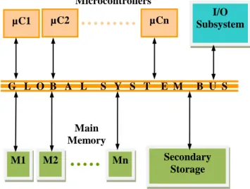
Microcontrollers µC1 µC2 µCn SubsystemI/O M1 M2 Mn Secondary Storage Main Memory G L O B A L S Y S T E M B U S
Fig -1: Generic Architecture of Multi-Micro Controller System
___________________________________________________________________________________________________ process has in recent years been raised towards the system
level. Design Space Exploration (DSE) is a key ingredient of such system-level design, during which a wide range of design choices are explored, especially during the early design stages [14]. Therefore, such early design choices heavily influence the success or failure of the final product, and we can avoid wasting time and effort in further design steps without the possibility of meeting design requirements because of an inappropriate system architecture design.
2. GENERIC ARCHITECTURE OF
MULTI-MICROCONTROLLER SYSTEM
Theoretical models of parallel embedded systems are abstracted from the physical models. These models are often used by algorithm designer and VLSI device/Chip developers. The ideal model provides a convenient framework for developing parallel algorithms/hardware without worry about the implementation details or physical constraints [10]. A generic architecture of multi-microcontroller system is shown in fig. 1. There are number of microcontrollers are connected in parallel to a shared bus interface. Input/output sub systems and memory segment are also connected to this shared bus.
3.
DESIGN
(NoC)
MODEL
OF
MULTI-MICROCONTROLLER SYSTEM
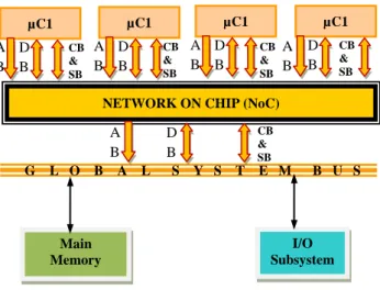
To synchronize the local system buses to the global system buses NoC is inserted between the global system bus and local system buses. A clear view of the system with NoC is shown in fig. 2. The operating speed i.e. the switching capability should match with the four microcontrollers. As in our case the number of microcontrollers is four.
Networks-on-Chip (NoCs) were proposed as the solution to
shared bus scalability issues, emerging as the new parading for designing scalable communication infrastructures in SoCs. The main advantage of a NoC over a shared bus is its capability to reduce design costs while providing high-performance communications. In a NoC, each microcontroller is connected by a Network Interface (NI) to a network link [3]. Those links are point-to-point data lines connected with other links via switches. A link can connect a switch with another switch or with a NI, in such a way that there exists direct or indirect connection between any two cores. Due to the similarities between interconnection networks and NoCs, it is possible to borrow concepts and techniques from the former and apply them to NoCs. Even so, most of the techniques developed for interconnection networks cannot be directly applied in NoCs, while other ones would be completely unaffordable using current technologies [15]. The reason for this lies in the restrictions imposed by each environment. For example, while in interconnection networks buffers are a relatively abundant and affordable resource; in NoCs they are scarce and expensive, with high area requirements and power consumption, which hinders even more their use in NoCs. On the contrary, links are an expensive resource in interconnection networks that must be used with austerity, while in NoCs links are more abundant. Additionally, the total area available and the tolerable power consumption budget of a SoC are very limited. An ideal NoC must meet the communications needs of the design while minimizing power and area consumption. This latter fact implies that the switches should be as fast, small and power-efficient as possible, which hinders even more the application of interconnection solutions in NoC designs. The architecture of each NoC component directly or indirectly affects all kinds of design parameters, like maximum operating frequency, buffering requirements, etc. The compilation of architectures of the components that compose the network is referred as network architecture.
4. RELATED WORK AND DESIGN ANALYSIS
There are four latches for address bus, data bus, control bus and status bus. Only address bus is unidirectional and rest is bi-directional. So the complexity of address bus is less as compare to the others. The modeling and designing of intelligence latches are done. The latches shown in fig.6 has been successfully simulated and synthesized on Zynq-7000 by Xilinx Vivado 2013.4.
4.1 RTL Modeling of Latch for Address Bus
Latch_Address:
Port ( Clk_in : in STD_LOGIC;
LAdd_in : in STD_LOGIC_VECTOR (15 downto 0); TriStateBuffer_En : in STD_LOGIC;
LAdd_Out : out STD_LOGIC_VECTOR (15 downto 0) );
begin
if (Clk_in'event and Clk_in = '1') then Temp_Add <= LAdd_in; end if; end process; µC1 I/O Subsystem Main Memory G L O B A L S Y S T E M B U S NETWORK ON CHIP (NoC)
Microcontrollers
Fig -2: Design Model of Multi-Microcontroller System AB: Address bus, DB: Data Bus,
CB&SB: Control Bus & Status Bus A B D B CB & SB µC1 A B D B µC1 A B D B µC1 A B D B CB & SB CB & SB A B D B CB & SB CB & SB
___________________________________________________________________________________________________ CTRL_BUFFER: process (TriStateBuffer_En, Temp_Add)
begin if (TriStateBuffer_En = '1') then LAdd_Out <= Temp_Add; --- --- end process;
4.2 RTL Modeling of Latch for Data Bus
Latch_Data: Port (
Clk_in : in STD_LOGIC;
TriStateBuffer_En : in STD_LOGIC; Latch_DB_DIR :in STD_LOGIC;
LData_In_LGSB : in STD_LOGIC_VECTOR (7 downto 0); LData_Out_LGSB : out STD_LOGIC_VECTOR (7 downto 0);
LData_In_GSBL : in STD_LOGIC_VECTOR (7 downto 0); LData_Out_GSBL : out STD_LOGIC_VECTOR (7 downto 0) ); begin --- --- end process;
CTRL_BUFFER1: process (TriStateBuffer_En, Temp_Data, Latch_DB_DIR)
begin
if (TriStateBuffer_En = '1' and Latch_DB_DIR = '0') then LData_Out_LGSB <= Temp_Data; ---
--- end process;
CTRL_BUFFER2: process (TriStateBuffer_En, Temp_Data, Latch_DB_DIR)
begin
if (TriStateBuffer_En = '1' and Latch_DB_DIR ='1') then LData_Out_GSBL <= Temp_Data; ---
---
end process;
4.3 RTL Modeling of Latch for Control Bus
Latch_control: Port (
Clk_in : in STD_LOGIC;
Latch_CB_DIR :in STD_LOGIC; TriStateBuffer_En : in STD_LOGIC;
LCtrl_In_LGSB : in STD_LOGIC_VECTOR (5 downto 0); LCtrl_Out_LGSB : out STD_LOGIC_VECTOR (5 downto 0);
LCtrl_In_GSBL : in STD_LOGIC_VECTOR (5 downto 0);
LCtrl_Out_GSBL : out STD_LOGIC_VECTOR (5 downto 0) ); begin --- --- end process;
CTRL_BUFFER1: process(TriStateBuffer_En, Temp_Ctrl, Latch_CB_DIR)
begin
if (TriStateBuffer_En = '1' and Latch_CB_DIR = '0') then LCtrl_Out_LGSB <= Temp_Ctrl;
--- --- end process;
CTRL_BUFFER2: process(TriStateBuffer_En, Temp_Ctrl, Latch_CB_DIR)
begin
if (TriStateBuffer_En = '1' and Latch_CB_DIR ='1') then LCtrl_Out_GSBL <= Temp_Ctrl; --- --- end process;
4.4 RTL Modeling of Latch for Status Bus
Latch_Status: Port (
Clk_in : in STD_LOGIC; Latch_SB_DIR :in STD_LOGIC; TriStateBuffer_En : in STD_LOGIC;
LStatus_In_LGSB : in STD_LOGIC_VECTOR (1 downto 0);
LStatus_Out_LGSB : out STD_LOGIC_VECTOR (1 downto 0);
LStatus_In_GSBL : in STD_LOGIC_VECTOR (1 downto 0);
LStatus_Out_GSBL : out STD_LOGIC_VECTOR (1 downto 0) ); begin --- --- end process; CTRL_BUFFER1: process(TriStateBuffer_En, Temp_Status, Latch_SB_DIR) begin
if (TriStateBuffer_En = '1' and Latch_SB_DIR = '0') ---
___________________________________________________________________________________________________ --- end process; CTRL_BUFFER2: process(TriStateBuffer_En, Temp_Status, Latch_SB_DIR) begin --- --- end process;
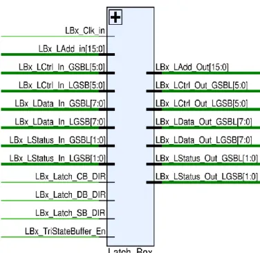
5. LATCH BOX
To reduce the complexity of the system by the above discussed latches. We have introduced a component, known as latch box. In latch box all latches are integrated to form a component which is later used in the multi-microcontroller system.
RTL Modelling of Latch Box Port (
LBx_Clk_in : in STD_LOGIC;
LBx_TriStateBuffer_En : in STD_LOGIC;
LBx_LAdd_in : in STD_LOGIC_VECTOR (15 downto 0); LBx_LAdd_Out : out STD_LOGIC_VECTOR (15 downto 0);
LBx_LData_In_LGSB : in STD_LOGIC_VECTOR (7 downto 0);
LBx_LData_Out_LGSB : out STD_LOGIC_VECTOR (7 downto 0);
LBx_LData_In_GSBL : in STD_LOGIC_VECTOR (7 downto 0);
Fig-3: RTL Schematic of Latch Box
LBx_LData_Out_GSBL : out STD_LOGIC_VECTOR (7 downto 0);
LBx_Latch_DB_DIR : in STD_LOGIC;
LBx_LStatus_In_LGSB : in STD_LOGIC_VECTOR (1 downto 0);
LBx_LStatus_Out_LGSB : out STD_LOGIC_VECTOR (1 downto 0);
LBx_LStatus_In_GSBL : in STD_LOGIC_VECTOR (1 downto 0);
LBx_LStatus_Out_GSBL : out STD_LOGIC_VECTOR (1 downto 0);
LBx_Latch_SB_DIR : in STD_LOGIC;
LBx_LCtrl_In_LGSB : in STD_LOGIC_VECTOR (5 downto 0);
LBx_LCtrl_Out_LGSB : out STD_LOGIC_VECTOR (5 downto 0);
LBx_LCtrl_In_GSBL : in STD_LOGIC_VECTOR (5 downto 0);
LBx_LCtrl_Out_GSBL : out STD_LOGIC_VECTOR (5 downto 0);
LBx_Latch_CB_DIR : in STD_LOGIC);
6. RESULTS
6.1
Utilization Graph
Fig -4: Utilization Graph
6.2
Utilization Table
___________________________________________________________________________________________________
6.3
Behavioral Simulation of Latch Box
Fig-5: Behavioral Simulation of Latch Box
___________________________________________________________________________________________________
6.4
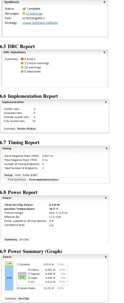
Synthesis Report
6.5
DRC Report
6.6
Implementation Report
6.7
Timing Report
6.8
Power Report
6.9
Power Summary (Graph)
Fig -7: Power Summary
6.10
Implemented Design
Fig -8: Implemented Design
7. CONCLUSIONS
In the above result design of latches namely address, data, control and status for multi microcontroller embedded system on programmable chip is successfully done. Also the designed latches are integrated into a single component i. e. latch box. This latch box with different latches will be used in the multi-microcontroller-system-on-programmable-chip for the synchronization of address bus, data bus, control bus and status bus to the shared bus which is global system bus. The prototyping & verification has been done using following tools & technology by considering various design constraints:
Software operating environment:
Operating System: UBUNTU 14.04 LTS
Hardware Design Software: Vivado 2013.4
Modeling and Simulation Software: Vivado 2013.4
Synthesis Software: Vivado 2013.4
Static Timing Analyzer: Vivado 2013.4
Power Analyzer: Vivado 2013.4
Power Estimator: Vivado 2013.4 Hardware Prototyping Environment:
FPGA Device: Zynq-7000 (Ultra-Fast and Ultra-Low-Power)
Zynq-7000 FPGA Device Series: xc7z020clg484-1
Device Technology: 28nm
Device Category: General Purpose
Clock Frequency: 50 Hz to 1GHz
Speed Grade: -1
No. of Pins: 484
Operating Voltage: 1.16 V
Operating Temperature: -200 C to 800 C
___________________________________________________________________________________________________
REFERENCES
[1]. Benini, L. and De Micheli, G., 2002. Networks on Chips: A new SoC paradigm. IEEE Computer, 35(1), 2002; 70-78.
[2]. Terry Tao Ye 2003. On-Chip Multiprocessor Communication Network Design and Analysis PhD thesis, Stanford University.
[3]. Francisco Gilabert Villamon, 2011. Design Space Exploration for Networks On-chip. PhD thesis Universitat Polit`ecnica de Val`encia
[4]. Beltrame G., Sciuto, D., Silvano. C., Paulin, P.and Bensoudane,E.,2006. An application mapping Methodology and case study for multi-processor on – chip architectures. Proceeding of VLSI SoC 2006. 16-18 October 2006, Nice. France 146-151.
[5]. T. S. Rajesh Kumar 2008. On-Chip Memory Architecture Exploration of Embedded System on Chip PhD thesis Supercomputer Education and Research Centre Indian Institute of Science, Bangalore, India.
[6]. Uday Arun, A. K. Sinha, 2012. A Design Space Exploration of Binary-Tree-Decoder For Multi-Block- External-Memory-Controller in Multi-μc Embedded Soc Design. International Journal of Engineering Inventions, Volume 1, Issue1, August 2012.
[7]. John Kim, James Balfour, and William Dally. Flattened Butterfly Topology for On-Chip Networks. In MICRO ’07: Proceedings of the 40th Annual IEEE/ACM International Symposium on Microarchitecture, pages 172–182, Washington, DC, USA, 2007. IEEE Computer Society.
[8]. F. Poletti, D. Bertozzi, A. Bogliolo, L. Benini, "Performance Analysis of Arbitration Policies for SoC Communication Architectures", Journal of Design Automation for Embedded Systems, pp.189-210, Vol. 8, June/Sep 2003.
[9]. A novel on-chip communication network .Proceeding of International Symposium on System-on-Chip, 16-18 November 2004.
[10]. Kai Hwang (2008). Advance Computer Architecture, Parallelism, Scalability, programmability. McGraw-Hill Companies Inc. New York.
[11]. Jerraya, A. and Wolf W., 2005. Hardware-software interface co-design for embedded systems. Computer, 38(2), February 2005; 63-69.
[12]. Angiolini, F., Ceng, J., Leupers, R., Ferrari, F., Ferri, C., and Benini, L. 2006. An integrated open framework for heterogeneous MPSoC design space exploration. In Proceedings of the Design, Automation and Test in Europe (DATE'06), 1145-1150.
[13]. Erbas, C. 2007. System-level modeling and design space exploration for multiprocessor system-on-chip architectures. PhD thesis, Amsterdam University Press, Amsterdam, the Netherlands.
[14]. Jia, Z. J., Pimentel, A. D., Thompson, M., Bautista, T., and Nunez, A. 2010. NASA: A generic infrastructure for system-level MPSoC design space exploration. In Proceedings of the IEEE 8th
Workshop on Embedded systems for Real time Multimedia, 41-50.
[15]. G. Benini L., De Micheli. Networks on Chips: Technology and Tools. Morgan Kaufmann, 2006. [16]. http://www.arm.com
BIOGRAPHIES
He did his B. Tech. in Electronics and Telecommunication Engineering from UPTU, Lucknow. M. Tech. (pursuing) in Electronics and Communication Engineering from UPTU, Lucknow. His research interests include Embedded System Design, System-On-Chip Design.
She did her B. Tech. in Electronics and Communication Engineering from Bundelkhand University, Jhansi, and M. Tech. in VLSI Design from UPTU, Lucknow. Her research interests include VLSI Design.