Bi-directional power converters for smart
grids
Isolated bidirectional DC-DC converter
Welday Gebremedihn
Gerekial
Master of Science in Electric Power Engineering
Supervisor: Tore Marvin Undeland, ELKRAFT
Co-supervisor: Nils Backman(Dr.), Eltek company
Submission date: June 2014
Galvanic Isolated Bidirectional DC
Resonant Converter
Welday Gebremedihn Gerekial
Master of Electrical Power Engineering Submission date: June 2014
Supervisor: Tore Marvin Undeland (Prof Co-supervisor: Backman Nils
Norwegian University of Science and Technology
Department of Electric Power Engineering
Galvanic Isolated Bidirectional DC-DC LLC
Resonant Converter
Welday Gebremedihn Gerekial
Master of Electrical Power Engineering Prof.)
ersity of Science and Technology
Department of Electric Power Engineering
Problem Description
Most activities in the world depend on the electrical power system so that uninterrupted power supply is needed. In most cases reliable power is stored in batteries. This can be expanded to supply the ac system by the same battery. This can be achieved by the application of power electronics with bidirectional power converters. Isolated bidirectional dc-dc LLC resonant converter is one of the building blocks that enable power to flow in both directions. The converter is static to be used in battery charging and discharging circuits for uninterruptable power supply, hybrid vehicles, space application, telecommunication, hospital etc.
LLC resonant converter is a promising alternative for converters to reduce switching losses and to improve the life time of the MOSFETs. LLC resonant converter reduce or eradicate the energy circulating in the converter by applying zero voltage switching and zero current switching. The converter should be analyzed by simulation to the LLC resonant tank in the isolated bidirectional converter and also the efficiency of the bidirectional converter should be tested in the laboratory. Develop the automatic controller, small signal analysis and minimize the loss by selecting the proper resonant value. If time, the converter should be developed and tested on laboratory.
The goal of the thesis is to minimize the switching loss of the MOSFETs by adding the LLC resonant tank on the isolated bi-directional dc-dc converter and also improve the lifetime efficiency of the converter. In addition to develop LLC resonant tank in the isolated bidirectional converter also develop automatic bi-directional controller.
Assignment: Trondheim 10.01.2014 Supervisor: Tore Marvin Undeland(Prof.) Co-supervisor: Backman Nils
Abstract
As part of my master thesis I have take part in Isolated Bidirectional DC_DC LLC resonant converter from Eltak company. Application of power exchanges takes place in either direction using two unidirectional DC-DC converters. Even though it is common to use power flow in unidirectional, but later due to many application growing emphasis on small size, compact the two unidirectional way of power flow and efficient power systems. This gives increasing interest to develop a bidirectional type of power flow with bidirectional converter. This is especially for DC power application like motor drives, uninterruptible power supplies(UPS), alternate energy system, telecommunication, space technology, hybrid Automotives, battery charger and battery discharger.
After a literature study of different types of converter topology , the isolated bidirectional DC-DC LLC resonant converter has been selected. This resulted in LLC resonant tank have for both mode of operation. The converter is dual active bridge with isolated high switching frequency transformer. The bridge on the high side is voltage-fed and current-fed on the low side of the converter.
Since the isolated bidirectional DC-DC converters have the capability to perform the bidirectional power flow in a compact form or a single device to perform such application. Therefore for this specialization project it is proposed to have dual full-bridge isolated bidirectional DC-DC LLC resonant converter in a compact and single device converter. The topology computable for this type of isolated bidirectional DC-DC converter. In this bidirectional converter mainly discussed about the role LLC resonant arrangement instead of PWM for reducing power loss in high switching frequency.
Acknowledgements
I would like to express my gratitude and appreciation to my supervisor Prof. Tore Marvin Undeland for his constant encouragement, guidance and support during whole period of time stay on NTNU for the thesis and other supporting courses.
I would like also to thank to my co-supervisor Dr. Backman Nils for his guidance and excellent participation in topology selection and further discussions on different specifications. He was also committed for supporting in lab work by send some lab components.
Furthermore, I would like give my appreciation to ELKRAFT power electronic lab staff members for their open welcome to help in laboratory equipment arrangement. I would like appreciate my colleague master student for creating pleasant work environment at the reading room.
At the last I would like to gratitude thanks my wife and my close friend for their support during my study.
Table of Content
Problem Description ... i Abstract ... ii Acknowledgements ... iii List of Figures ... vi Chapter 1-Introduction ... 1 1.1 General Introduction ... 11.2 The Art of Bi-Directional DC-DC Converter ... 2
1.3 The Need For Galvanic Isolation ... 5
1.4 Literature Review ... 7
1.5 Thesis Structure outlines ... 9
Chapter 2- LLC Resonant Converters ... 10
2.1 Introduction ... 10
2.2 Three Most Common Resonant Topologies ... 10
2.3 LLC Resonant Converter ... 18
2.4 Operation of LLC resonant converters ... 19
2.5 System Optimization For LLC Resonant Converter ... 20
2.6 Operation principle of LLC Resonant Converter ... 21
Chapter 3- Isolated Bi-Directional DC-DC Converter ... 24
3.1 Introduction ... 24
3.2 Topology of Bi-directional DC-DC LLC resonant converter ... 24
3.3 Operation of the converter and simulation results ... 26
3.4 Backup/Current Fed Mode ... 34
Chapter 4- Small Signal Analysis ... 40
4.1 Introduction ... 40
4.2 State Space Approach ... 41
4.3 Considered Assumptions for Simplifying Small Signal Model ... 41
4.4 Small signal analysis for charging mode of operation ... 42
4.5 Small Signal Analysis For discharging Mode of Operation ... 59
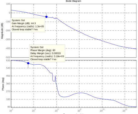
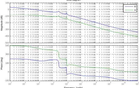
4.6 Frequency Response From Small Signal Analysis ... 62
Chapter 5- Designing Power Component And Controller ... 65
5.2 Design of LLC resonant components ... 68
5.3 Gate driver design ... 72
Chapter-6: Experimental results ... 76
6.1 Introduction ... 76
6.2 Charging mode ... 76
Chapter-7: Conclusion and Recommendations for future work ... 78
7.1 Conclusion ... 78
7.2 Suggestion for future works ... 78
Reference ... 79
List of Figures
Fig.1- 1 Illustration of bidirectional power flow ... 2
Fig.1- 2 Constructing non-isolated bidirectional DC-DC converter from two unidirectional converter ... 3
Fig.1- 3 Basic structure of isolated bidirectional DC-DC converter ... 5
Fig.1- 4 Effect of galvanic isolation in circuit. ... 6
Fig.2- 1 Full-bridge series resonant converter ... 11
Fig.2- 2: DC-gain characteristics of SRC resonant converter ... 12
Fig.2- 3: Full-bridge parallel resonant converter ... 14
Fig.2- 4: DC-gain characteristics of PRC resonant converter ... 15
Fig.2- 5: Full-bridge series parallel resonant converter ... 16
Fig.2- 6 : DC-gain characteristics of SPRC resonant converter ... 17
Fig.2- 7: LLC resonant converter topology ... 18
Fig.2- 8: DC characteristics of LLC resonant converter ... 19
Fig.3- 1: High voltage side with voltage-fed converter and with low side current-fed ... 25
Fig.3- 2: Bidirectional DC-DC converter in step-down mode of operation ... 26
Fig.3- 3:Wave forms for the charging mode of operation ... 28
Fig.3- 4: Converter operating in the forward mode in the interval T1-T2 ... 29
Fig.3- 5: Converter operating in the forward mode in the interval T1-T2 ... 30
Fig.3- 6: Converter operating in the forward mode in the interval T2-T3 ... 31
Fig.3- 7: Converter operating in the forward mode in the interval T3-T4 ... 32
Fig.3- 8: Voltage and current output in charging mode ... 33
Fig.3- 9: Bidirectional DC-DC converter in step-up mode of operation ... 34
Fig.3- 10: Wave forms for the discharging mode of operation ... 35
Fig.3- 11: Converter operating in the reverse mode for T3-T4 interval ... 36
Fig.3- 12: Converter operating in the reverse mode for T3-T4 interval ... 37
Fig.3- 13: Converter operating in the reverse mode for T3-T4 interval ... 38
Fig.3- 14: Converter operating in the reverse mode for T3-T4 interval ... 38
Fig.3- 15: Voltage and current during discharging mode of operation ... 39
Fig.4- 1: The block diagram of the system including feedback. ... 41
Fig.4- 2: Equivalent circuit with two resonant tank ... 43
Fig.4- 3: Equivalent circuit with transferred resonant to primary side ... 43
Fig.4- 4: Equivalent circuit with equivalent resonant banks on the primary side of the converter ... 44
Fig.4- 5: Switch form of full-bridge inverter ... 47
Fig.4- 6: The large signal modeling of sine and cosine components ... 52
Fig.4- 7: step response of linear dynamic model ... 54
Fig.4- 8: Output voltage step response with full-bridge converter ... 55
Fig.4- 9: Output voltage step response of the non-liberalized dynamic model ... 55
Fig.4- 10:Controlled output voltage ... 58
Fig.4- 12: Open loop bode plot for backward mode ... 64
Fig.5- 1: The circuit design for full-bridge rectifier with capacitor filter ... 66
Fig.5- 2: output voltage for both a)without and b) filter capacitor ... 66
Fig.5- 3: Gate driver circuit design for half-bridge switch control ... 73
Fig.6- 1: Converter in discharging mode of operation ... 76
Fig.6- 2: a) CH1: Vab 250V/div, CH2: Vcd, and b) CH1 and CH2 are gate driver signal to S1 and S2 and CH3 and CH4 to S3 and S4 respectively with 10V/div ... 77
Chapter 1-Introduction
1.1 General Introduction
The world now is going to exercise the power electronic applications device for complex systems when most difficulty face for human being in many stream of fields. Over the last three to four decades power efficiency become the main concern of researches for power conservations as a result these leads to grow compact power supplies grows significantly. Power electronics circuits primarily process the energy supplied by utility or storage devices to a form which matches with required load or storage device through the application of semiconductor devices to control the voltage and current values . The energy can supplied from utility grid or bank of batteries; with the application ranging from high power conversion equipment of MW to the very low power equipment of a few watts.
Most of power converter devices have common unidirectional application with power being supplied from the source to the load. However different types of applications require dual direction; the applications such as motor drives, uninterruptible power supplies(UPS), alternate energy system, telecommunication, space technology, hybrid Automotives, battery charger and discharger etc. require using another system of conversion which is not similar to unidirectional. Therefore these applications introduce power converter with bi-directional power transfer property.
Conventionally, the two independent unidirectional converters can be used together parallel for achieving bi-directional power transfers. Bidirectional DC-DC converters recently gates awareness due to application of bidirectional power transfer between different dc sources buses. The demand for development of complex, compact and efficient power system implementation has encouraged scientists in bi-directional converter development.
1.2 The Art of Bi-Directional DC-DC Converter
1.2.1 Introduction to Bidirectional dc-dc converter
Most bidirectional DC-DC converter topologies can be illustrated as block diagram shown in the Fig-1.1 below and it also characteristics power flows in both directions[1-3]. Energy storages in general uses bidirectional DC-DC converter for charging and discharging applications may be either in half-bridge or full-bridge arrangement of semi-conductor switching devices. The buck type of converter has energy storage on the high voltage side, whereas boost type of converter has energy storage on the low voltage side.
The concept of power flow in both direction for bidirectional dc-dc converter is operation of switching devices realize current flow in each way. Bidirectional dc-dc converters are developed from two unidirectional semiconductor switching devices such as; MOSFET, Transistors and IGBT power switches constructed with parallel diodes. These parallel diodes serves double sided power flow. Even though there are many topologies of bidirectional dc-dc converter; basically they are divided into two types such as an isolated bidirectional DC-DC converters and non-isolated bidirectional DC-DC converters based on the isolation material between input and load[4-6].
Bi-Directional
DC-DC converter
I1 I2 + V2-
+
V1-
Backward power Flow
Fig.1- 1 Illustration of bidirectional power flow
1.2.2 Non-isolated Bidirectional DC-DC Converter
Non-isolated bidirectional DC-DC converters power flow without any isolation between input and load[7]. The transformer-less non-isolated dc-dc converters can be either boost, buck or buck-boost converters. Even though it's attractive to obtain isolation[8-9] for high frequency conversion applications between the load and the source but non-isolated type of converter is more attractive from the efficiency, size, weight and cost point of view.
The most familiar DC-DC converters, such as buck and boost converters have only one direction power flow. Since step-up and step-down converters contain diode on their structure which has characteristic of one direction power flow. However it has advantageous to change unidirectional converter into bidirectional by replacing the diodes with controllable switches like MOSFETs and IGBTs. As Fig.1-2 shows that the structure of converter is a combination of two unidirectional step-up and step-down converters. So that the unidirectional converters are transferred into bidirectional converters by replacing the diodes with controllable switches like MOSFETs and IGBTs [10] shown in unidirectional dc-dc converters.
Some of the limitations relating to the Non-isolated bidirectional dc-dc converter compared to isolated bidirectional dc-dc converters shown in the above Fig.1-2 are:
● It can only operate boost mode in one direction and buck mode in the other direction. This means the voltage duty ratio(D) , which is defined as D = Vo/Vin, is either smaller
than one or equal to one in one direction. This indicated the voltage level of dc-dc converter is determined by the arrangement of the switch device and filter devices.
● When the voltage ratio become very large this shows not practical.
● Due to lack of galvanic isolation between the two sides of the network if a short circuit risk happened on one side of the system; the whole system of the DC-DC converter will be failed.
1.2.3 Isolated Bidirectional DC-DC Converters
The transformer is used for isolating bridge converters which is on both sides of DC-DC converters or it isolates input and load. While the transformer has additional cost in addition to the component cost; however it has critical component for isolating the source and load by providing impedance matching between the two sides and prevent a short circuit occurred on one side of the enter system. Isolated bidirectional DC-DC converters can be classified as full-bridge, a half-bridge or push-pull bidirectional converters[11-12] based on the arrangement of the switching devices and their application.
Generally bidirectional converters have a structure similar to the Fig. 1-3. The topology consists of two high switching frequencies DC-AC and AC-DC converters with similarly high frequency transformer which is primarily used to maintain the galvanic isolation between the sources. Therefore the topology consists both rectifier and inverter on either of its bridges. Since the transformer has a numbers of turns on both sides then it is essential for voltage matching between the two sources. As an energy is transferred in either direction is required for the enter system, therefore each side of the converter must have a capability to transfer in both direction using controlling system.
Fig.1- 3 Basic structure of isolated bidirectional DC-DC converter
As the term bi-directional indicates, there are basically two mode of operations where the of switches either turned-off or turned-on in order to control power flow from either direction. As Fig.1-3 shows the two mode of operations are noted as charging/step-down and discha step-up detail will be discussed in chapter-3. Notification of the power transfer can be differ from publication to publications. There are different isolated bidirectional dc-dc converter publications[20-22].
1.3 The Need For Galvanic Isolation
Transformer isolation needs for a system when there is no need of direct connection between source and load. If there is no an isolation between the load and the source, a single circuit fault occurred on any circuit component of the system has high probability to damage the entire system. If two fault develop anywhere in the system, a current path will exist among
faults therefore a short circuit occurred on the converter. For this case it need to either to a controller or add transformer isolation device in order to interrupt power system during fault minimize the current due to the fault which damage components before the protective controlling functions are activated. But if we place the isolated galvanic components between the source and load then these problems and faults can be minimized even eradicated the fault at all. Thus, the system will remain powered-on and not damaged the system entirely. Current fault path will be happened if there are multiple faults on one side of the isolation zone. It is therefore very advantageous to have galvanic isolation for almost all loads. Fig.1.4 shows the above effects of either we have galvanic isolation or not, X indicates there is a fault on the short circuit area
1.4 Literature Review
The first step towards maximizing the performance of isolated bidirectional DC-DC converter is to review the limitation of the existing systems. These converters were the focus of significant research interest over the last four ten years. In this section, previous works in the area of bidirectional DC-DC converter is reviewed with the objective of current and voltage status of research in this specialization project evaluating topologies for their possible implementation in low power LLC bi-directional DC-DC converters.
1.4.1.High power bidirectional dc-dc converter
Various topologies variations for DC-DC converters of high power applications with bidirectional power transfer have been proposed and developed through the last four decades. For the development of the efficient power, dc-dc converter they use either resonant[13], soft switch achieved by controlling phase shift [14-16], or hard pulse width modulation(PWM)[17]. Even though PWM and soft switched achieved by controlling phase shift converters have their own advantages but they have also limitations to use for middle power bidirectional dc-dc converters. These converter topologies aren't efficient to use for middle bidirectional dc-dc converters due to the following drawbacks;
● large number of switches
● large components
● limited range of satisfactory for high frequency
● complex power and control circuit etc.
Operation of the converter in series resonant converter[13] is seen as high power densities and has the advantage of natural commutation and soft switching ability. However they have limitations in terms of frequency sensitivity, higher voltage and current stresses in the devices of the topologies and large ripple currents in the output and input capacitive filters. Resonant converters also require careful selections for matching the operation frequency of the resonant tank circuit, and magnetic saturation.
The dual bridge presented [14] achieves lower switching losses by controlling the phase shift between the two inverting stages operating at high frequency. It uses the leakage inductance of the transformer as the main energy transfer component. At high level power and frequencies design and implementation of transformer and controlling the leakage is extremely complicated[14].
1.4.2 Medium and low power bidirectional dc-dc converter
As a high power applications, medium and low power bidirectional dc-dc converters are based on either hard switching[16], soft switching or resonant switching type[19]. Most of these dc-dc converters are well suited for a particular application even though they have their own drawback. Their limitations can be described as;
● lack of isolations
● high component stresses
● large ripple current through the filtering inductors
● at high frequencies the converter designed to operate under resonance and soft switching may suffer from hard switching of the devices.
The converters operating in the resonance modes[19] have the limitation on the load and voltage conditions and also subject the devices to high stresses. The presence of only one active switch in the circuit path during each direction of power flow leads to a higher rate for the switch and component as a whole results increase cost. In addition conduction losses in the resonant part also increase due to their series arrangements. The bidirectional converter topology designed in [19] does not provide galvanic isolations between the battery and the load or source which is often required in battery operated power systems.
1.5 Thesis Structure outlines
This thesis is organized as follows:
Chapter 1 gives a general over view on different bi-directional DC-DC converter and give the
application of different bidirectional topologies in DC-DC converter. In general DC-DC converters are classified as isolated and non-isolated bi-directional. Bi-directional DC-DC converters can be constructed with a series of two-stage DC-DC converter with an isolation of transformer between them. The selected topology for this dc-dc converter is isolated bi-directional dc-dc LLC resonant converter.
In Chapter 2 gives an over view of three type of resonant converter arrangement. The chapter also detail discuss about each arrangement about their advantage and disadvantages. Based on the application of these resonant converters the most efficient and serve for reducing circulating energy within the converter is LLC arrangement of the resonant tank.
Chapter 3 presents detailed components of the dual full-bridge bi-directional DC-DC LLC
resonant converter. This also includes the circuit and simulation results for both operation modes; that is charging mode of operation and discharging mode of operation. Charging mode of operation gives more detail in step-down and the discharging also deals with step-up from the battery or other source to the main grid. This chapter also includes design of the digital circuit for MOSFET gate drive signal controller. Efficiency of isolated bi-directional DC-DC resonant converter is almost 97%.
Chapter6 discuss the small signal analysis and develop the controlling system of the converter
and in addition drive the transfer function of the plant and the system. The controller type also selected.
Chapter5 The capacitor filter design and calculated the capacitor value based on the specific
ripple factor Rp. Also design the gate driver and the bootstrap-of the controller.
chapter 6 describe the experimental result of the converter for forward and backward mode of
Chapter 2- LLC Resonant Converters
2.1 IntroductionHigh power, efficiency and density are the major core cause for the development of new resonant converter. These converters are called LLC resonant converters which solve the drawbacks of the previously known series and parallel resonant converters will discuss in detail in this chapter. Based on their fusibility, these resonant converters developed due to their ability of higher switching frequencies, higher efficiencies, simple and small packaging. These are also the paths considered for the development and manipulating of the LLC resonant converter[23]. Within all these issues a topology capable of higher switching frequency with higher efficiency will be achieved. The goal of resonant converter is solving the limitation of the hard switching and PWM switching that produces high loss will be minimized to a very small value.
The most earlier resonant converter which was investigated mostly around three decades ago [23-24], but later the power loss faced in DC-DC converters were resolved due to the implementation of these resonant converter topologies to operate at high switching frequencies. In general traditional trend of resonant converter topologies can be classified into three major classes. The classification is based on the arrangement of the resonant components; Series Resonant Converter, Parallel Resonant Converter and Series Parallel Resonant are the three most popular topologies.
2.2 Three Most Common Resonant Topologies 2.2.1 Series Resonant Converter
In this case, the dual active full-bridge switch topology is connected to the series resonant converter on both sides of the transformer as shown in the Fig.2-1. The resonant inductor Lr and Resonant capacitors are series connected with active full-bridge MOSFETs switches . They form a series resonant tank which is serially connected to load so that the resonant tank and load are voltage dividers where as the load is reflected from secondary to the primary side of transformer. It is possible to control the impedance of the resonant tank by varying the switching frequency of input voltage.
Since the impedance of the resonant tank and loads are voltage divider, the gain of the voltage ratio or voltage gain to this type of resonant tank is always less than one. At resonant frequency impedance of the series resonant tank will be insignificant and as a result the voltage drop across the resonant is not considered in the analysis. Therefore at the resonant switching frequency the voltage gain almost have unity value.
Fig.2- 1 Full-bridge series resonant converter
The general code developed in appendix[A1] generates value for the parameter of the resonant tank(i.e. Lp, Cp, Ls, and Cs). The developed code interface with simulink developed plant output
voltage and switching frequency. The generated values of the resonant tank parameter value are selected if they satisfay the required resonant frequency. From Fig.2-2 the parameter values are Lp = 335.8µH, Ls = 28.8µH, Cs = 392nF and Cp = 13.5µF.
The parameters value for this series isolated bi-directional resonant converter are specified as follow:
Transformer turn ratio: 25:3 Input voltage: 400V Rload : 0.8Ω
From Fig.2-2 selecting the appropriate value of the resonant parameters from the right side of the resonant frequency is recommended operating regions of the resonant tank to have high efficiency. For high efficient resonant converter the loss is consider for the selection of the operating region, so that zero voltage switching region is the appropriate range. This is due to the law loss during zero voltage switching(ZVS) and MOSFETs application in DC-DC converter. If the region selected for the operation is on the left side; then the switching frequency is lower than the resonant frequency the converter will work under zero current switching(ZCS) condition.
From Fig.2-2 characteristic of DC-gain, the DC gain slope is negative then the converter is under zero voltage switching condition, but when the DC gain slope is positive the converter is under the condition of zero current switching. But due to the internal structure of the MOSFET is advisable to operate the resonant converter under the ZVS region. Referring to Fig-2.2 the operating region for small load implies high switching frequency in order to have a constant output voltage. This is a main drawback and limitation for the SRC.
Based on the above analysis SRC is not appropriate structure of the resonant tank for DC-DC converter. Its main limitations are: in light load regulation and high circulating energy.
Fig.2- 2: DC-gain characteristics of SRC resonant converter
0.8 0.85 0.9 0.95 1 1.05 1.1 1.15 1.2 1.25 0 0.1 0.2 0.3 0.4 0.5 0.6 0.7 0.8 0.9 1 f s/fr Vo /V in 6 8 10 12 14 16
2.2.2 Parallel Resonant Converter
The schematic circuit diagram for the PRC is shown in the Fig.2-3 and the arrangement of the capacitor and inductor are still similar as described in SRC, when they are compared with the arrangement of resonant tank components. The only difference is the arrangement of capacitor with load, where capacitor in parallel resonant converter is parallel to load but series in series resonant converter. More familiar names for this converter can be called as a series resonant converter with parallel load impedance.
As described in the series resonant converter the general code developed in appendix[A2] generates value for the parameter of the resonant tank(i.e. Lp, Cp, Ls, and Cs). The developed
code interface with simulink developed plant output voltage and switching frequency. The generated values of the resonant tank parameter value are selected if they satisfay the required resonant frequency. From Fig.2-4 the parameter values are
Lp = 543.8µH, Ls = 12.8µH, Cs = 4522nF and Cp = 225µF.
The parameters value for this parallel isolated bidirectional resonant converter are specified as follow:
Transformer turn ratio: 25:3 Input voltage: 400V Rload : 0.8Ω
Resonant frequency: 100KHz
The dc-gain characteristic of the resonant converter is shown in Fig.2-4. As shown in the figure the dc-gain characteristic(Q) of the PRC is ranging from 4 to zero.
Fig.2- 3: Full-bridge parallel resonant converter
As shown on Fig.2-2 in the SRC operating region is very narrow with small load but the switching frequency is very high and make difficult to have almost constant and regulated output voltage. But PRC has a wider operation region with light load and very small switching voltage variation. Therefore it has an advantage to have constant and regulated output voltage. At high input voltage the converter is working at higher frequency even far away from the resonant frequency values.
PRC still faces some limitations in circulating energy which occur during small load. So that the load is parallel with resonant capacitor in the input side of the isolation part with small value impedance even at no load condition. Even though parallel resonant converter have better range of operation but still have the above limitations. Therefore Parallel resonant converter is not preferable similar to series resonant converter in dual active full-bridge bidirectional DC-DC converter and this lead to another alternative option to solve the limitation.
Fig.2- 4: DC-gain characteristics of PRC resonant converter 2.2.3 Series Parallel Resonant Converter
SPRC merges the above two resonant topologies together and its resonant bank consists of three components, such as series resonant inductor(Lr), series resonant capacitor(Csr) and parallel resonant capacitor(Cpr). Its schematic diagram is shown in the Fig.2-5. The resonant tank of SPRC is constructed from both structures, series resonant converter and parallel resonant converter. This combination leads to minimize the limitation in each resonant topology separately. The Combination of these two structures of SPRC can regulate the output voltage even at no-load conditions.
The dc-gain characteristic(Q) of the series parallel resonant converter is mirror of the LLC resonant converter which will see in detail in the next section of this chapter.
0 0.2 0.4 0.6 0.8 1 1.2 1.4 1.6 1.8 2 0 0.5 1 1.5 2 2.5 3 3.5 fs/fr Vo /V in 0.2 0.4 0.6 0.8 1 2 4
Fig.2- 5: Full-bridge series parallel resonant converter
As discussed in the two different topologies above; they have a circulating energy and turn off-current for switches (in this case MOSFETs) face drawback at high input voltage. Even though SPRC arrangement structure of the capacitor and inductor reduce the problems on one but not for the second, still it has a high conduction loss and switching loss at wide input voltage. While SPRC has limitation of wide range input voltage design; In this wide range of voltage input the conduction loss and switching loss will dramatically increase at high input voltage, so the switching loss is very approach to PWM converter at the same level input voltage.
Then it is possible to generalize based on the above drawback of designing on SRC, PRC and SPRC difficult to optimize at high input voltage due to high conduction loss and switching loss. So that, to achieve high switching frequency and higher efficiency researchers developed another type of topology called LLC (resonant Inductor, resonant capacitor and magnetizing inductor)[28].
2.3 LLC Resonant Converter
The above three traditional resonant topologies have many limitations during the high voltage input. Their main limitations are high circulating energy and large switching loss which are occurring during the high voltage input. From Fig.2-7 LLC resonant can be designed by interchanging the position of the L to C and C to L from LCC arrangement of inductor and capacitors in series parallel resonant converter. Here there are two resonant frequencies: Lr and Cr determine the higher resonant frequency and the lower resonant frequency which is determined by the series combination of inductance Lr and Lm with Cr[28].
Fig.2- 7: LLC resonant converter topology
Even though the LLC resonant converter existed for a very long time, its lack of understanding of the characteristics of the converter helps to serve as a series resonant converter with passive load. In other words it is designed to operate at switching frequency which is much higher than the resonant frequency of the series resonant tank of Lr and Cr; but in series and parallel resonant converter switching frequency is equal to the resonant frequency. Advantages of LLC resonant converter compared to the above three traditional resonant converters has a narrow switching frequency range with light load and ZVS capability with even no no-load.
2.4 Operation of LLC resonant converters
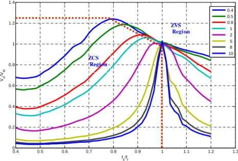
LLC resonant converter have zero voltage switch(ZVS) and zero current switch(ZCS) regions of DC characteristics as shown in the Fig.2-7. For LLC resonant converter have two types resonant frequencies due to parallel arrangement of one inductor; one is determined by the resonant components of Lr and Cr and the second type of resonant frequency is produced due to Lm and Cr. The frequencies can be analysis as the following equations:
1 =
√
(1)
2 =
(2)
''LLC DC characteristics is sketched and analyzed , take samples for 400V input operation; it could be placed at the resonant frequency of fr1, which is the resonant frequency of the seriescomponents of the LLC resonant converter(i.e. Lr and Cr)[25]. As shown in Fig.2-8 low switching frequency and large DC characteristics are obtained as input voltage decreases.
Fig.2- 8: DC characteristics of LLC resonant converter
0.4 0.5 0.6 0.7 0.8 0.9 1 1.1 1.2 1.3 0 0.2 0.4 0.6 0.8 1 1.2 1.4 fs/fr Vo /Vin 0.4 0.5 0.8 1 2 5 8 10 ZCS Region ZVS Region
2.5 System Optimization For LLC Resonant Converter
The practical results show that PWM converters have drawback to achieve high efficient and large operation ranges. The LLC resonant converters solve the drawback of PWM due to exhibit of high performance in small voltage stress and low switching loss on rectifier side of the converter and this results lead to have higher efficient than PWM converter.
2.5.1 Improve MOSFETs Selection For High Frequency Resonant Converter
For high-voltage MOSFET's, it is better to select high quality switches such as super-junction MOSFETs which offers low Rds. Infineon's CoolMOS have such quality for low switching loss
and high efficiency[29]. It is necessary to discuss the performance of the convectional MOSFET's in this application before deciding to use Infineon CoolMOS in LLC resonant converter.
Under low-load situation the switches become unable to fully recover, therefore large recovery current can cause the switches to breakdown and lead the failure of the system. The unique Infineon MOSFET quality is to overcome these unable recovery in low load using its internal intrinsic diode structure of switches. The special property of Infineon super-junction MOSFET's solve the conventional drawback in low-load reverse current by applying different path for the reverse current[30]. Even though the failures is recovered by the MOSFET's intrinsic diode property, but the reverse recovery current drops the efficiency of resonant converter.
Since the current through the convectional switching device and the reverse voltage are very small , this lead the MOSFETs to fail in the primary full-bridge side. This small reverse voltage is not sufficient for the conduction of the within this short conduction period. Since in super-junction MOSFETs the P-doped column is added to the N-epi region, the P-column serves as balancing the charge at the conduction channel and this gives the device to have high concentration of doping with the same blocking voltage[29,31]. The higher concentration of doping in N-epi leads high conduction or low on-resistance in the super-junction MOSFETs. The P-column serves to have enough time for reverse current flow and solve the drawback of the convectional MOSFETs in reverse current leads to failure of the device.
2.6 Operation principle of LLC Resonant Converter
As described in the above sub-sections LLC resonant converter topology has reduced magnetizing inductance than the series and parallel resonant converter. The less magnetizing inductance in LLC resonant realize soft switching for the primary side switches. As shown in Fig.2-10 dc-voltage characteristic gain can be grater or less than one. From these voltage gain curves, the switching frequencies are normalized by the resonant frequency which is developed in chapter-4 and represented as:
=
1
2 √
Fig.2-10 dc-voltage gain characteristic for LLC resonant converter
From Fig.2-10 due to its different probability operation of LLC resonant converter, it is complex to gate the operational frequency of the converter. This happened if the converter haven't controlling feedback from the output. According to switching frequency of the LLC resonant operation can be classified as above, below and equal to resonant frequency[32, 33].
0.4 0.5 0.6 0.7 0.8 0.9 1 1.1 1.2 1.3 0 0.2 0.4 0.6 0.8 1 1.2 1.4 fs/fr Vo /Vin 0.4 0.5 0.8 1 2 5 8 10 ZCS Region ZVS Region
The general code developed in appendix[A3] generates value for the parameter of the resonant tank(i.e. Lp, Lmp, Cp, Ls, Lms, and Cs). The developed code interface with simulink developed
plant output voltage and switching frequency. The generated values of the resonant tank parameter value are selected if they satisfay the required resonant frequency. From Fig.2-10 the parameter values are:
Lp = 6.5µH, Ls = 93nH, Lmp = 71.5µH, Lms = 1µH, Cs = 27.25µF and Cp = 391nF.
The fixed value are similar to the series and parallel resonant converter as defined above.
2.6.1 Switching Frequency equal to resonant frequency
Series and parallel resonant converter are operated where resonant frequency equal to switching frequency increase the efficiency of the converter as described in the above sub-section. Furthermore the magnetizing component of the resonant converter modifies the voltage gain characteristic. In SRC and PRC, the ZVS operation region ensures for designing margins during design stage, however the converter is an able to operate at this operational region.
In LLC resonant converters, ZVS region has not limitation of operation. Therefore ZVS can be achieved for any switching rages that is either higher or lower than the resonant frequency. Here in LLC resonant converter no need of designing for margin, so that the converter can be operated with resonant frequency to achieve high efficiency for the converter.
When the switching frequency is equal to the resonant , the converter has achieved zero voltage switching for the primary full-bridge sides. However the switches turn-off current has very high magnetizing inductor current. These high switching magnetizing current can be reduced by choosing suitable magnetizing inductor, which reduces turn-off losses. Two of secondary full-bridge intrinsic diodes are either turned-on or turned-off with low di/dt. This refers the intrinsic diodes have small recovery loss.
Therefore, the resonant converter has high efficiency when its switching frequency is equal to resonant. From Fig.2-10, output and input voltages are virtually connected together. The resonant converter has also one voltage gain.
2.6.2 Switching Frequency greater than resonant frequency
If the LLC resonant converter operates with the range of switching frequency greater than the resonant frequency, the converter has similar property as the series resonant converter SRC. In forward mode of operation with this range of switching frequency, ZVS on the primary full-bridge switches is occurred due to high turn-off current. But this large turn-off current results for high loss while the secondary intrinsic full-bridge diodes have large di/dt ratio. Due to high di/dt ratio during the turn-off the diodes are under the pressure of voltage stress, which make the converter less reliable for application.
Therefore, the resonant converter has less efficiency when it is compared with the switching frequency which is equal to the resonant. From Fig.2-10, output and input voltages are virtually connected together. The resonant converter has lower than one voltage gain. However, as it shown in the figure the LLC resonant converter can achieve gains larger, equal or less than to one.
2.6.3 Switching Frequency less than resonant frequency
If the LLC resonant converter operates with the range of switching frequency lower than the resonant frequency, the converter has similar property as the parallel resonant converter PRC. Similar to the above two sub-sections the converter is able to achieve gain(Q) smaller, higher or equal to 1.
Chapter 3
-Isolated Bi-Directional DC-DC Converter
3.1 Introduction
This chapter present detail description on the selected bi-directional DC-DC converter described in chapter-2 for telecommunication application. At the beginning the topology evaluation for full-bridge current-fed and voltage-fed are the selected topologies[34]. Then the working principle of the converter will be discussed in both cases; discharging and charging mode of operation will be discussed. Each mode of operation will be followed by simulation result and all the simulation results are obtained by LTspice, Power Electronic Simulator(PSIM) and Mat-lab Simulink.
3.2 Topology of Bi-directional DC-DC LLC resonant converter
As mentioned in the introduction( i.e. chapter one) different types of bi-directional dc-dc converter types are categorized. Non-isolated Buck-boost, and isolated dual active full-bridge are typically known topologies in bidirectional dc-dc converters. Dual active full-bridge isolated bi-directional dc-dc converter is the proper selection for this paper with LLC resonant converter. Isolated dual active full-bridge type of bi-directional topology has the following advantages over non-isolated buck-boost bidirectional dc-dc converters:
• Electrical isolation between input and output is guaranteed; system protection is possible when output load short circuit takes place
• Higher step-up ratio can be implemented due to the transformer turn ratio which is impossible in practical for duty ratio
• The transformer can be served as storage energy and balancing the impedance variations between two side etc.
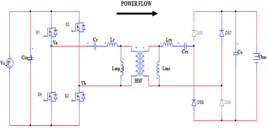
For these reasonable and other advantages isolated full-bridge topology is preferable to select for bi-directional dc-dc LLC resonant converter. The dual active full-bridge isolated bi-direction dc-dc LLC resonant converter topology is sketched in Fig.3-1. Full-bridge topology of isolated bi-directional dc-dc LLC converter contains two active switch bridge on both sides of the transformer. The active switch bridge on the high voltage side is fed by utility while the low side
voltage is fed by current source for charging mode of operation and reverse for discharging mode of operation.
The LLC resonant converter is placed on both sides of the full-bridge. The LLC resonant type of topology has high quality to reduce losses due to circulating energy within the converter leads for balancing the impedance on both sides of the isolations and prevents net flow of current from any side of the isolation[35]. Therefore the LLC resonant converter prevents losses due to energy circulation both in the transformer and full-bridge switch.
Fig.3- 1: High voltage side with voltage-fed converter and with low side current-fed From Fig.3-1 due to low voltage, high current and high switching frequency as a result primary and secondary side full-bridge switches are selected as MOSFET's. Since the switching frequency of the converter is ranged from 100KHz to 150KHz, it is suitable to select MOSFET's for this dc-dc converter rather than IGBT's which are applicable for high voltage and low switching frequency. The full-wave bridge inverter and rectifier contains eight MOSFET switches in total for dual active full-bridge.
Implementing power MOSFET's in bi-directional dc-dc converter in the inverting side of converter zero voltage switching is required. Since the converter has MOSFETs it need Zero
current switching by adding series inductor-resistor component to the output in order to block the current flow through the intrinsic diode of the MOSFET's[38].
High and medium power bi-directional dc-dc resonant converters contain both LLC resonant and transformer isolation and these use to minimize overshoot voltage during switching transition from on-state to off-state. These have also the ability of zero voltage switching due to energy stored in resonant and transformer leakage inductances[36].
3.3 Operation of the converter and simulation results
The isolated bidirectional LLC resonant converter has two modes of operation shown in Fig.3 In the charging mode power flow from the dc-bus utility to battery or load but in the discharging mode of operation power flow from the battery to the dc-bus when power interruption
the source.
3.3.1 Charging mode of operation
In LLC resonant bidirectional dc-dc converter at the step down mode of operation power flows shown in Fig.3-2. The 400V voltage source step-down to 48V output either to load or battery depending on the application of the converter. In this mode of operation the resonant components implements zero voltage switching and zero current switching application[37].
In this mode energy flow from the DC-source to battery or load of the application. Switches S1,
S2, S3 and S4 gate signal from the controller while intrinsic diodes in S5, S6, S7 and S8 serves as
rectification of the sinusoidal source to the load and Fig.3-2 and Fig.3-3 indicates the operation of charging mode. The dc source supplies power to dual active bridge converter and then to the battery or load. The input voltage is step down by the transformer and either the battery is charged or the load gates a nominal voltage Vout. The MOSFET S1, S2, S3 and S4 on the primary
full-bridge side have gate signals with less than 0.5 duty cycle due to dead time added to the controller, while diodes of S5, S6, S7 and S8 give rectification purpose for this mode of operation.
This dead time is important to overcome the short circuit that occur during over lapping of time rise and time fail of the MOSFET's.
The operation of the converter is in every period of Ts and it has four stages operation for each switching time with the following time intervals; T0-T1, T1-T2, T2-T3, and T3-T4 intervals as
shown in Fig.3-3.
Interval T0-T1:
From Fig.3-3 either S1, and S2 or S3 and S4 are switching alternatively. For this duration of time
both S1, and S2 switches-off while S3 and S4 are turn-on . At time T0 S3 and S4 are gating rise
while S1, and S2 failed from on-state due to the dead time interval. In this interval the switches
either rising or fail due to delay and rise or fail time of the MOSFET's. The primary side of full-bridge output voltage; Va fails from dc-bus voltage to zero and Vb rise from zero to dc-bus
voltage. Since the transformer is not inverted the intrinsic diodes in the MOSFET's in S5, S6,
gates off-state while the S7 and S8 are on-state. The currents in the primary LLC-resonant bank
gates fail to its negative bus-current. The output filter component is only capacitor which filters the rectified signal to the battery or load. The energy stored from the previous interval in the resonant and magnetizing inductors provides the load or battery power.
Fig.3- 4: Converter operating in the forward mode in the interval T1-T2
Interval T1-T2:
Fig.3-5 shows that the circuit operation of the converter with this time interval. Switch S are turned-on at the instant of T1 and switches S1, and S2 turn-off, while the second bridge
switches remain turn-off. Similar to the first time interval the energy stored in the inductors supplies power to the load or battery. The primary side of full-bridge output voltage; Va
but Vb is equal to dc-bus voltage. Since the transformer is not inverted the intrinsic diodes in the
MOSFET's in S5, S6, gates off-state while the S7 and S8 on-state. Since the voltage across the
inductor is reverse, the inductor current decrease. These provides the intrinsic diodes in second full-bridge switches Ds5 and Ds6 are reverse biased since the primary side switches S1 and S
not conducting while Ds7 and Ds8 are forward biased. The diodes gate product of turn ration and
Fig.3- 5: Converter operating in the forward mode in the interval T1-T2
Interval T2-T3:
Fig.3-6 describes the converter signal diagram during this time interval. The operation of the resonant converter is similar to the time interval T0-T1 where S1 and S2 rise switches-on while
S3 and S4 are go-down until T3. The switches are linearly rise or fall due to the intrinsic semi
conductor structural property of the switches. Therefore the switches in nature never change state directly from on-state to off-state or alternatively. Since the switches have time rise and fall they change the state linearly.
The primary side of full-bridge output voltage; Va rise from zero voltage value to dc
voltage but Vb go-down from dc-bus voltage to zero. Since the transformer is not inverted the
intrinsic diodes in the MOSFET's in S5, S6, gates on-state while intrinsic diodes in S7 and S
Fig.3- 6: Converter operating in the forward mode in the interval T2-T3
Interval T3-T4:
The converter operation in this case is similar to the time interval T1-T2. The first half-bridge of
the primary sides(i.e. S1 and S2) are turn-on, while the S3 and S4 switches are turn-off.
shows the circuit operation of the converter with this time interval. Switch S1 and S2 are turned
on at the instant of T3 and switches S3, and S4 are turn-off, while the second bridge switches
remain turn-off.
Reverse to the T1-T2 time interval energy is storing in the inductors from the supplies power bus voltage supply. The primary side of full-bridge output voltage; Vb is zero but Va is equal to dc
bus voltage. Since the transformer is not inverted the intrinsic diodes in the MOSFET's in S turns to off-state while the S6 and S5 turn-on. Since the voltage across the inductor is forward the
inductor current increase and provides the intrinsic diodes in the second full-bridge switches Ds and Ds8 are forward biased whereas the primary side switches S3 and S4 are switched-on while
Ds5 and Ds6 are Reverse biased. The diodes gate product of turn ratio and magnetizing current
Fig.3- 7: Converter operating in the forward mode in the interval T3-T4
Voltage and current output:
The proposed isolated bi-directional DC-DC converter validates proposed high efficiency power flow. Fig.3-8 indicates the simulation result of the converter with selected values of the parameter from the given specification, selected materials and selection of the parameters of the resonant component from previous chapter LLC resonant.
Fig.3.8 shows that the DC-DC converter has high efficiency with small ripple of the Vbat
The ripple value of output voltage and current is less than 1% and its Efficiency is around Which is high achievement in decreasing the ripple as well as excellent efficiency for extending the life time of the converter components specially for MOSFETs.
As mentioned in the earlier chapter, zero voltage switching and zero current switching benefits of LLC resonant in the converter. Therefore the converter will be reduced conduction loss during the freewheeling cycle during the high voltage-side of the full switch due to zero voltage switching application.
Fig.3- 8: Voltage and current output in charging mode 3.3.2 Forward mode of operation with flux imbalance
The four time intervals described are considered as ideal without considering flux imbalance. Therefore the dual active full-bridge bi-directional converter in the forward mode of operation is considered with balanced flux between the two sides of the transformer. First it need to define the flux balance and saturation of transformer. If the average output voltage applied to the primary side of the transformer where the positive pulse is not the same as the negative pulse for each cycle the transformer flux balance can't be occurred. Therefore the transformer flux density increase with the number of cycle and finally flux density saturation occurred. Gradually the saturation of the transformer goes to the slope of hysteresis curve. The magnetizing inductance of the transformer increases with the proportion of hysteresis curve and finally gates saturation and burns down the switching MOSFET's and gate drive controlling components.
The node voltages at the junction A and B each contains half cycle DC-bus voltages may not be the same. This condition of the full-bridge output voltage may result in saturation of the
5.47 5.48 5.49 5.5 5.51 5.52 5.53 5.54 5.55 5.56 x 10⁵ 46 48 50 52 54 56 58 60 62 Time(s) Vb a t a n d Io Io Vbat
transformer core metal and sever the switching MOSFET's . Fig.3-1 shows that the resonant tank serves for balancing the voltage difference between each half cycle output voltage .
3.4 Backup/Current Fed Mode
The converter operates in discharging mode of operation when dc-bus supply power is interrupted. In the lack of dc-bus power supply the battery start discharge in order to supply for the rest of power network. Fig.3-9 shows the step-up from 48V to 400V where the battery is the source of the power. The secondary full-bridge switches S5, S6, S7 and S8 are active participate
for this mode of operation and the first full-bridge switches S1, S2, S3 and S4 are always off
but their intrinsic diodes are participate in rectification.
Fig.3- 9: Bidirectional DC-DC converter in step-up mode of operation
The duty ratio of the bidirectional is not exactly 0.5 due to the switch intrinsic component property. Therefore from the graphic characteristic of the MOSFET's they have approximately 0.45 duty ratio due to smoothly rise and fall of the MOSFET's. Rectification at the output is carried out by intrinsic MOSFET diode's of S1, S2, S3 and S4 switches. The step-up mode is
described with the wave-form shown in Fig.3-10. As described in the step-down or charging mode of operation the resonant and magnetizing currents are assumed continuous. The wave form describes in the time interval between T0 and T4 for the converter operation within a period.
Fig.3- 10: Wave forms for the discharging mode of operation
Interval T0 - T1:
Switches S5 and S6 are on the turn-on state before the time instance of T0 and then after time
begun to fall-down until T1 ; while switches S7 and S8 on the off-state before the time instance of T0. The converter circuit diagram at this time interval is difficult to identify due to its intrinsic
property of the MOSFET's all have transition period either from on state to off-state or vice versa. The secondary transformer winding subject to magnetizing inductor, which stores energy that appear across the battery. From Fig.3-10 the inductor currents increase with second order or parabolic graph which shares equally by S7 and S8 switches. During this time interval the energy
The energy is transferred to the dc-bus from the battery by S7 and S8 switches intrinsic Diode
rectification. The DS7 and DS8 intrinsic diodes are conducting while DS5 and DS6 are subject
reverse biased.
Fig.3- 11: Converter operating in the reverse mode for T3-T4 interval
Interval T1 - T2:
S7 and S8 at instant T1 continue to remain on-state while S5 and S6 are turned-off during this
interval of time which is clearly described in Fig.3-12. From the waveform shown in Fig.
energy stored in the Inductors during the two previous intervals then provides load power to the dc-bus by rectification through the intrinsic MOSFET's diode of the primary full-bridge side. Since the power flow to the dc-bus, the inductor linearly decrease until T2 time interval.
In this time interval Vc is zero but Vd is equal to dc-battery voltage. Since the transformer is not
inverted the intrinsic diodes in the MOSFET's in S1, and S2, gates off-state while the DS
DS4 intrinsic diodes are turned on. Thus, they have the same current flow through the intrinsic
Fig.3- 12: Converter operating in the reverse mode for T3-T4 interval
Interval T2 - T3:
Fig.3-10 shows that interval T2 - T3 have similarity with T0 - T1 interval. S5 and S6 switches gate
signal from gate drive and turn from off-state to on-state, while S7 and S8 switches turned from
on-state to off-state due to the intrinsic property of MOSFET's. Since S5 and S6 are going turned
on the inductors core store energy with second order rise of current, which is not the same as the above interval with linear rise of current. Voltage across node C rises linearly from zero at Vbat at T3, similarly Vd decreases linearly from Vbat to zero with corresponding time.
Fig.3- 13: Converter operating in the reverse mode for T3-T4 interval
Interval T3 - T4:
The converter circuit operating during this time interval is shown in Fig.3-14. The wave form of the signal is similar to T1- T2 time interval. As shown in the wave form for this time interval the
inductors store energy due to conducting of S5 and S6.
Voltage and current output:
In the forward mode of operation the output voltage and current detailed discussed. Here the difference is the change of power from battery to the DC-bus source. The proposed isolated bi-directional DC-DC converter validates proposed high efficiency power flow. Fig.3-15 indicates that the simulation result of the converter with selected values of the parameter from the given specification, selected materials and selection of the parameters of the resonant component from previous chapter LLC resonant tank.
Fig.3.15 shows that similar to forward mode of operation the converter has high efficiency with small ripple of the Vs and Is. The ripple value of output voltage and current is less than 1% and
its efficiency is around 97%. This is great achievement in decreasing the voltage and current ripple therefore this prototype is better choice for extending the life time of the converter components specially for MOSFETs.
The benefits of LLC resonant in the converter as mentioned in the earlier chapter is zero voltage switching and current switching. Therefore the converter will be reduced the conduction loss during the freewheeling cycle during the high voltage-side of the full-bridge switch due to zero voltage switching application.
Chapter 4- Small Signal Analysis
4.1 Introduction
The converter circuit parameters and their rating values are analyzed at steady state in chapters two LLC resonant topology. The output voltage of the resonant converter is controlled as the output load and input voltage vary by regulating the switching frequency value in DSP-controller to drive the MOSFETs in new frequency. Therefore the dynamic change of output voltage of the converter can be accomplished by applying feedback control from output to the error compensator as shown in Fig.4-1[39].
The compensated error amplifier compares' the reference value with the feedback or current value in order to modify switching frequency of gate drives in the resonant converter. In order to design the compensator; developing mathematical expression of the converter plant at dynamic performance is the basic tool for developing the controller of the converter. Therefore the dynamic performance of the resonant converter plant can be expressed in small signal transfer function using; harmonic function, extended describing function and steady state expressions. These transfer function of the plant uses to design the compensate error amplifier(controller); which gives to control overall system based on dynamic response of the system.
The isolated bi-directional dc-dc LLC resonant converter system shown in Fig. 4-1 contains two transfer functions; Gp(s) is the Laplace-Domain transfer function of the plant that is the resonant
converter and Gc(s) is the controller transfer function which control the output voltage by
Fig.4- 1: The block diagram of the system including feedback.
This chapter describes the small signal analysis for both forward and backward mode of operation. The transfer function of the system is developed under voltage control mode which also used to analyze and design of the compensator under the closed control loop.
4.2 State Space Approach
In nature power supply from switching devices are not linear; so that they are discontinuous which needs techniques in order to linear the system and the circuit can be analyzed. State space modeling is the best way to tackle the non-linear system[40-41] by approximating the non-linear operating points to linear mathematical expression.
State space modeling is mathematical expression of non-linear operating points in linear expression by considering some approximations or assumptions. The state space averaging approach described in [40-42] are use to derive the open loop and control loop transfer function. There are some assumption for driving the transfer function in the next sub-topic.
4.3 Considered Assumptions for Simplifying Small Signal Model
The assumptions for simplifying the performance of the resonant converter in small signal modeling with the following procedures.
The output ripple is negligible.
The switching devices are instantaneous switching from state to state using the first harmonic method.
4.4 Small signal analysis for charging mode of operation
In forward mode the small signal analysis starts by transferring secondary circuit parameters to the primary side by using turn ratio of transformer. The transfer operations are secondary resonant inductor, resonant capacitor, magnetizing resonant inductor and load. In general there are four steps to analyze the forward small signal[42], which are described as follow:
1) State the time variant non-linear state equations 2) Harmonic approximation
3) Applying extended describing function 4) Developing the states space Model
4.4.1 State the time variant non-linear state equations
As described in the considering assumption to analysis small signal is simplifying the construction of the converter by using ideal switching device. To have simplified topology of the converter, then transferring the resonant tank from secondary to primary side will give non-complex approach for state equations analysis. The equivalent circuit for the resonant converter is built as the following three figures with the Vab square wave signal output of the first
full-bridge converter.
The simulation of the small signal is sampled for the first harmonic components because the assumption for simplifying the analysis of the small signal. Here are the steps to gate the final equivalent circuit signal design of resonant converter.
Equivalent circuit LLC Resonant Converter
Fig.4- 2: Equivalent circuit with two resonant tank
Vab AC-voltage with first harmonic peak value of the output from the primary full-bridge
converter
s(secondary), p(primary), mp (primary magnetizing component) and ms(secondary magnetizing component)
Transferring the secondary components of LLC resonant tank parameters to primary side of the transformer by using transformer turn ratio( = )
′ = ∗ ′ = ∗ ′ = ∗