Reset Circuits With Energy Recovery
for Solid-State Modulators
Juergen Biela, Member, IEEE, Dominik Bortis, Student Member, IEEE, and Johann W. Kolar, Senior Member, IEEE
„This material is posted here with permission of the IEEE. Such permission of the IEEE does not in any
way imply IEEE endorsement of any of ETH Zürich’s products or services. Internal or personal use of this
material is permitted. However, permission to reprint/republish this material for advertising or
promo-tional purposes or for creating new collective works for resale or redistribution must be obtained from
the IEEE by writing to
[email protected]
.
Abstract—In power modulators for pulses in the microsecond range, transformers are often used for generating high output voltages. With standard topologies, the transformer is usually only excited in a unipolar direction, i.e., the flux density B swings between zero and a value close to the saturation flux density. By applying a reset circuit, the flux densityB in the transformer is set to a value close to the negative saturation flux density before the pulse, so that the flux density could swing between the negative and positive saturation values during the pulse. This allows one to halve the core area and reduce the core volume/weight as well as the losses. In this paper, the operating modes of three different reset circuit topologies (the standard and a new advanced passive as well as an active one) and the corresponding waveforms are explained. Furthermore, the three topologies are compared with respect to the losses/complexity based on a design for a solid-state modulator with 20-MW output power and 200-kV output voltage.
Index Terms—Energy recovery, premagnetization, pulse trans-former, reset circuit, solid-state modulator.
I. INTRODUCTION
P
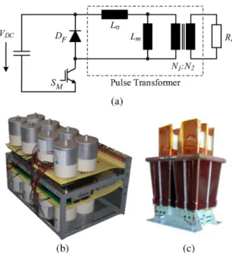
ULSED POWER systems are used in a wide variety of applications, for example, in particle accelerators, radars, medical radiation, sterilization systems (e.g., drinking water), or ion implantation systems (semiconductor manufacturing). In these applications, pulses of several kilovolts and megawatts are generated, and the duration of the single pulse varies from a few nanoseconds to some milliseconds. The requirements on the generated pulses regarding, e.g., rise/fall time, overshoot, pulse flatness, and pulse energy are high and can vary over a wide range. Therefore, many different topologies are applied in pulsed power systems [1]–[3].A lot of pulsed power systems (e.g., the one shown in Fig. 1) use a pulse transformer to step the output voltage up. The design of a pulse transformer is comparable to high-frequency (HF) transformers which are widely used in power electron-ics. However, in contrast to many converter topologies using HF transformers, pulse power systems only generate repeated unipolar voltage pulses. In this case, the core material of the pulse transformer is not optimally utilized.
The unipolar voltage pulse leads to a unipolar flux swing
ΔB1 in the core (cf. Fig. 2). This results in a core volume
approximately twice as big as with a bipolarΔB2 excitation. Manuscript received September 28, 2007; revised December 18, 2007. Current version published November 14, 2008.
The authors are with the Power Electronic Systems Laboratory, Eidgenoessische Technische Hochschule Zurich, 8092 Zurich, Switzerland (e-mail: [email protected]; [email protected]; [email protected]). Color versions of one or more of the figures in this paper are available online at http://ieeexplore.ieee.org.
Digital Object Identifier 10.1109/TPS.2008.2005265
Fig. 1. (a) Schematic of a solid-state modulator with IGBTs and photo of the (b) modulator(W×L×H= 45×25×35cm)as well as of the (c) transformer.
Fig. 2. Schematic magnetization curve with unipolar flux swingΔB1, bipolar flux swingΔB2(≈2×ΔB1), and negative premagnetizationBReset. This curve is derived from measured B–H loops of AMCC25 cores made of 2605SA1/Metglas.
A bipolar flux swing operation of the transformer could be achieved with a reset circuit which premagnetizes the core to a negative flux densityBReset(S2)before the pulse.
The most common method to reset transformer cores is the dc reset circuit (cf. Fig. 3), where a dc current is used to premagne-tize the core [4]. The current flows in a direction that generates a magnetic flux (cf.BResetin Fig. 2) which is in the opposite 0093-3813/$25.00 © 2008 IEEE
Fig. 3. Schematic of passive reset circuit. TABLE I
SPECIFICATION OF THECONSIDEREDPULSE
MODULATORWITHRESETCIRCUIT
direction than the flux induced by the voltage pulse. Therefore, a flux swingΔB2 from a negativeS2 to a positive operation
pointBMaxinstead of form zero (remanenceS1) to a positive
operation point is possible. This increases the total possible peak-to-peak flux swing ΔB2 by a factor of approximately
two compared to a circuit without reset circuit and results in a significant reduction of the core cross section/volume and of the winding losses due to shorter turn lengths.
Basically, this current can be supplied to the primary, sec-ondary, or tertiary windings. In order to keep the considerations more general, a tertiary winding, also called reset winding, is assumed in this paper.
During the operation, however, high losses (≈1.5 kW in the considered case) are generated since the energy stored in the magnetizing/leakage inductor and the energy stored during the pulse in the dc inductor are dissipated in the freewheeling diodeDF as explained in [4]. In order to recover part of the
losses, a new dc reset circuit is presented in this paper [5], which is based on low-voltage technology common, e.g., in automotive converters. With this circuit, the energy stored in the premagnetizing inductor could be fed back to the reset circuit supply. This results in significantly lower losses compared to the standard passive reset circuit.
The energy stored in the magnetizing/leakage inductance, however, is still dissipated in the freewheeling diode. In order to also recover these losses, an active reset circuit is required [6]–[8]. There, the energy stored in the inductors is largely re-covered to an additional capacitor and reused for premagnetiz-ing the transformer before the next pulse. This leads to a further significant reduction of the losses due to the premagnetization and an improved efficiency.
In order to judge the losses and component effort of these three reset circuit topologies, the efficiency and component stresses are compared for the specifications given in Table I in this paper. Furthermore, the basic operation principle is explained, which has not been done before in detail.
Fig. 4 Current paths for the passive reset circuit in the three time sections: premagnetization, pulse, and demagnetization. (a) Premagnetization. (b) Pulse. (c) Demagnetization.
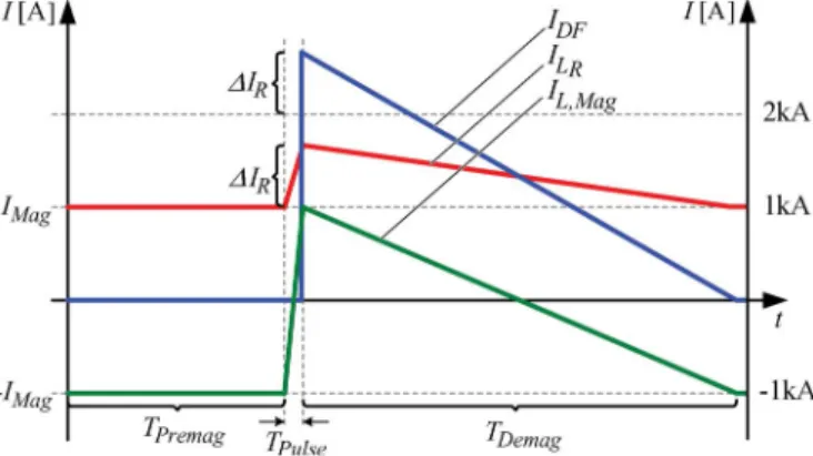
Fig. 5 Run of the currentIDFin the freewheeling diodeDF, the magnetizing currentIL,Mag, and the currentILRin the premagnetization inductanceLR.
First, the standard dc reset is described shortly in Section II. Then, the new improved passive reset circuit is explained in Section III, and the functionality of the active circuit is pre-sented in Section IV. After the explanation of the three circuits, the comparison of the losses and component stress is given in Section V. Finally, a conclusion and topics of future research are presented in Section VI.
II. PASSIVERESETCIRCUIT
In the following, the standard passive reset circuit shown in Fig. 3 is shortly explained (details can be found, e.g., in [4]). There and in the explanations of the advanced passive and active reset circuits, the influence of the leakage inductance is omitted since its influence on the efficiency is very small.
The circuit consists of a dc voltageVResetsource, an inductor LRwith relatively large inductance (usually in the millihenry
range), and the parasitic resistance RR of the inductor/third
winding. Due to the voltage source, a dc current flows through the inductor and the third winding, which premagnetizes the core negatively to BReset (cf. Figs. 2 and 4(a)). There, the
amplitude of the current is determined byVReset/RR.
As soon as the main switchSM is closed, the dc link voltage Vdc is applied to the primary winding NP, and the magnetic
flux density starts to rise fromBResettoBMax, which results in
a change of the magnetization current from−IMag=IResetto IMag(cf.TPulsein Figs. 4(b) and 5). Furthermore, the primary
voltage is not only reflected to the secondary but also to the tertiary winding. This leads to an increasing currentILR/stored
energy in the reset inductorLR ΔELR= 1 2LR (IR,T + ΔIR,T)2−IR,T2 . (1) There,IR,T is the reset currentIRon the tertiary side.
Fig. 6. Proposed advanced passive reset circuit.
Fig. 7. Current paths for the advanced passive reset circuit in the three time sections: premagnetization, pulse, and demagnetization. (Interlocking time is omitted for the sake of brevity.) (a) Premagnetization. (b) Pulse. (c) Demagnetization.
After the pulse, the magnetization current flows via the freewheeling diode. Additionally, the current inLR (reflected
to the primary due to the negativedi/dt) flows there, and the energy stored in the magnetizing inductanceLM as well as the
additional energy stored inLRdue to theΔIR,T (cf. (1)) must
be dissipated in the freewheeling diode until the initial state with constant premagnetization current is reached again.
With the considered specifications (cf. Table I), approxi-mately 90% of this energy is provided by the pulse source (dc link capacitor) and 10% by the sourceVReset of the
pre-magnetization. In order that the demagnetization ends before the next pulse, the forward voltage of the freewheeling diode
DF must not be too small. In the considered case, a forward
voltage of approximately 10 V (a series connection of four diodes APT DF430U10G resulting in a demagnetization time ofTDemag= 250μs) is assumed.
III. ADVANCEDPASSIVERESETCIRCUIT
In order to recover the additional energy stored in the premagnetization inductor LR,A during the pulse, the circuit
shown in Fig. 6 is proposed [5](RR,A=parasitic resistance).
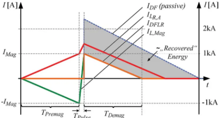
There, the core is premagnetized before every pulse by turning the two switchesSR1andSR2on (cf. Fig. 7(a)) and increasing
the amplitude of the magnetizing currentIL,Magup to the
nomi-nal value(IMag). During the premagnetization, the magnetizing
inductance and the inductorLR,Aare connected in series and
build an inductive voltage divider. In order to avoid a current flowing through DF during this period, it is important that
the voltage drop across the magnetizing inductance is smaller than the forward voltage of the (series connected) freewheeling
Fig. 8. Run of the currentIDF,LVin the freewheeling diodeDF, the mag-netizing currentIL,Mag, the currentIL,V in the premagnetization inductance
LV, and—for comparison—the current in the freewheeling diodeDF for the passive reset circuit explained in Section II. The area “Recovered” Energy is proportional to the energy which is recovered by the advanced passive circuit.
diode(s) DF. This also determines the minimal time for
pre-magnetization (Fig. 8).
At the end of the premagnetizing periodTPremagone or both
switches(SR1/SR2)are turned off, and shortly thereafter, the
main switchSM is turned on.
In case both MOSFETs are turned off, the magnetization cur-rent flows along the dashed green path via the diodesDR1and DR2shown in Fig. 7(b), and a small share of the energy stored
inLM andLR,Ais fed back to the sourceVResetin the
inter-locking delay between the switching actions. During the pulse, the currentILR,Acontinues to flow along the dashed green path
and adds to the switch current. Thus, the total switch current at the end of the pulse is load+magnetization current+ILR,A. In
analog manner, this is also true for the standard passive circuit. In addition, the currentILR,A increases with a largerdi/dt
than during the premagnetization since the voltage Vdc− VResetlies in the positive direction across inductorLR,Aduring
the pulse. Therefore, energy is transferred from the pulse source to the reset sourceVReset.
In case only one MOSFET is turned off, the current is free-wheeling via one diodeDRν and the turned on MOSFETSRν
instead of flowing via the voltage sourceVReset. Consequently,
the amplitude of the current ILR,A is approximately constant
before the main switch SM is turned on, and this state could
be used, e.g., for keeping the magnetization current constant until the pulse in case the nominal magnetization currentIMag
is reached before the pulse begins (e.g., due to tolerances). Another possibility is to keep the premagnetization current constant between the pulses (as with the standard passive premagnetization) if the time between the pulses is short (high repetition rate). During the pulse, turning off one MOSFET would lead to a higher di/dtthan turning off both, since the voltageVResetlies across inductorLR,A. In order to minimize
the energy stored inILR,A, it is assumed in the following that
both MOSFETs are turned off during the pulse.
As soon as the main switchSM is closed, the magnetization
current starts to rise from −IMag to+IMag. After the pulse,
the energy stored in the magnetization inductance is dissipated in the freewheeling diode DF, but the energy stored in the
premagnetization inductance LR,A is restored to the voltage
Fig. 9. Active reset circuit with energy recovery.
Fig. 10. Current paths for the active reset circuit in the three time sections: premagnetization, pulse, and demagnetization. (a) Premagnetization. (b) Pulse. (c) Demagnetization.
are significantly lower with this circuit than with the standard premagnetization circuit (cf. Section V), and the energy, which has to be provided by the sourceVReset, is relatively low.
IV. ACTIVERESETCIRCUIT
For further reducing the losses due to the premagnetization, an active reset circuit as shown, for example, in Fig. 9 could be applied [6], [8]. There, no passive components, like a pre-magnetization inductor, for voltage blocking/dividing or cur-rent control are utilized, and the transformer is premagnetized before each pulse.
For premagnetizing, the capacitor CR must be charged up
(e.g., by a boost converter as shown in Fig. 9) to a specific voltage level. In the considered case, 100 V(= 10% of Vdc)
is assumed. Then, the switch SR is closed, so that a
neg-ative premagnetization current starts to flow in the primary (cf. Figs. 10(a) and 11(a)). Energy is now transferred from the capacitor CR to the magnetizing inductance, and as soon
as the nominal magnetization currentIMagis reached, switch SR is turned off. As soon as switchSR is off, the current in
the leakage inductance freewheels via the dc link capacitor and the antiparallel diode of the main switch SM. Since the
negative voltage across the leakage inductance is relatively large (VLR=−Vdc), the current in the leakage inductance
decreases rapidly, and the current in the magnetizing inductance commutates to the secondary side. There, it flows via the load resistance, so that the voltage drop across the magnetizing inductance is relatively small (≈150 V in the considered case) and the magnetizing current decreases only slowly during this interlocking delay.
After the delay, the main switch is turned on, and the pulse is generated while the magnetizing current is ramping up from −IMag toIMag. There, no additional current from a
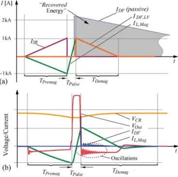
Fig. 11. (a) Ideal run of the current IDF,LV in the freewheeling diode
DF, the magnetizing current IL,Mag, the switch current ISR, and—for comparison—the current IDF resulting from the passive reset circuit (cf. Fig. 5). (b) Simulated waveforms for the diode currentIDF, the magne-tizing currentIL,Mag, the output voltageVOut, and the reset voltageVCR.
premagnetization inductor is flowing via switch SM as with
the two passive circuits and the current stress/losses inSM are
reduced.
After the pulse, the energy stored in the magnetizing in-ductance LM (and the part of the energy stored inLσ which
is not dissipated in SM while turning off) is fed back to the
reset capacitor CR via the freewheeling diode DF. Since the
reset capacitor voltage VCR is much larger than the forward
voltage of the diodeDF, the losses in the diode are small, and
the time for demagnetizationTDemagis short. Furthermore, the
freewheeling diodeDFcould consist of a single diode with low
forward voltage(=low losses)since the demagnetization time is mainly defined byVCR.
Due to the losses in the diode DF, the switch SR, the
damping resistor RR, and the transformer, the voltage across CR is a bit smaller after the energy recovery than before the
pulse. These losses/voltage drop can be compensated, e.g., by a boost converter, so that a symmetric flux swingΔB2around
zero is generated (cf. Fig. 2).
Another possibility is to use a slightly asymmetric flux swing for compensating the losses/voltage drop. In this case, the negative premagnetization amplitudeBReset(S2)(cf. Fig. 2) is
made a bit smaller than the positive oneBMax. Consequently,
also the negative magnetizing current amplitude is smaller than the positive one, and for premagnetizing the transformer, less energy is required than is stored in the magnetization inductance after the pulse. Therefore, more energy is fed back toCRthan is used for premagnetizing, which compensates for
the losses. This effect is self-stabilizing, i.e., the flux swing automatically shifts to a position, where the energy stored after the pulse is equal to the energy required for premagnetizing plus the losses.
a limit depending on the klystron specifications. The larger this value could be, the faster the pre- and demagnetization will take place.
This effect is also true for the two described passive reset circuits, but there, the negative voltage (defined by the for-ward voltage of the (series connected) freewheeling diodes) usually is smaller. This, however, also results in a longer pre-/demagnetization time.
In case the negative voltage is too large, a smaller volt-age VCR could be used. This results in a longer
pre-/demagnetization time and increases the losses.
During the pre- and demagnetization, the magnetizing induc-tanceLM is connected in parallel to the parasitic capacitances
of the transformer [9] and in series to the reset capacitorCR
and the leakage inductanceLσ. Due to the steplike excitation
by switchingSR, oscillations occur. By inserting the damping
resistor RD, the oscillations can be significantly damped as
could be seen in the simulated waveforms shown in Fig. 11(b). There, also the run of the capacitor voltage VCR, the load
voltage VOut, and the current IDF is shown. The waveform
of IDF shows a very short but high positive peak when SM
is turned off, which is caused by the current flowing through the leakage inductance Lσ, which has been neglected so far.
This current decreases rapidly since it flows via the loadRL
and causes only small losses.
The ringing shown in Fig. 11(b) are more damped in reality due to HF losses in the transformer, slower switches, and interconnection resistances which have not been considered in the simulation.
V. COMPARISON
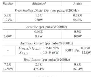
With all three circuits presented in the previous sections, a premagnetization of the transformer is basically possible. In order to compare the circuits, the losses and the component stresses have been calculated for a pulse modulator design shown in Fig. 1 operating with the specifications given in Table I. The resulting losses in the components are summarized in Table II.
In the case of the passive circuit, the 1.45-kW total loss result is mainly caused by the high losses in the freewheeling diode
DF. A share of 250 W of the total losses is caused in the
parasitic resistance RR of the inductor/transformer winding.
The calculated losses for the passive circuit correspond very well to measured losses, which are approximately 13% smaller due to component tolerances. Further measurement results will be presented in a future paper.
With the advanced passive circuit, the losses in the diodeDF
can be almost reduced by a factor of five, since the energy in the premagnetization inductorLR,A is recovered. In the auxiliary
circuit for controlling the current in the magnetizing inductance
LM and in the inductor LR,A, however, additional 150 W of
TABLE III
PROS ANDCONS OF THERESETCIRCUITTOPOLOGIES. (∗FORMINIMALLOSSES)
losses are caused in the diodes and 68 W in the MOSFETs. Therefore, only a reduction of approximately a factor of three is achieved for the total losses.
With the active reset circuit, the losses in diode DF can
be further reduced to 56.6 W. In the damping resistor RD,
however, significant losses of 100 W are generated, resulting in an improvement of approximately a factor of 8.5 regarding the overall losses compared to the standard passive circuit.
Besides the losses, also the amount of components and their stress is important for comparing the circuits. In Table III, different advantages and disadvantages of the circuits are sum-marized. There, it could be seen that the complexity of the passive circuit is low, but a third transformer winding and a high voltage inductor (>20 kV) are required for achieving the values shown in Table II. Basically, an operation without a third winding is possible but this does not result in minimal losses [4]. Furthermore, the forward voltage of the freewheeling diode must be high (short time for demagnetization/high repetition frequency), which leads in total in a relatively large volume for the reset circuit, which is also caused by the additional cooling effort.
With the advanced passive circuit, the complexity increases, but no third winding is required, and the losses/cooling effort are lower. The forward voltage of diode DF and the current
rating of the switchesSV1,2(∼75−100V/ >1-kA peak),
how-ever, must be high. Due to the required inductor and the auxiliary circuit, the system volume is again high.
A lower system volume could be achieved with the active circuit where mainly the capacitorCR(e.g., 750μF/100 V/1 kA
in the considered case) determines the size. Also, the complex-ity of the circuit is lower than with the advanced passive one. However, the switchSRmust have a high voltage and current
rating (1700 V />1 kA peak) as well as the single freewheeling diode DF. Additionally, the main switch SM must have an
antiparallel diode, so that the current in the leakage inductance could flow via the dc link capacitor and the freewheeling diode after switchSR has been turned off and before switchSM is
turned on.
Remark on costs: For the two passive circuits, a high for-ward voltage of the freewheeling diode is required (=series connection of three diodes in the considered case), and for the active circuit, a low forward voltage is sufficient(= 1diode). For the active circuit, however, a high voltage/current switch (here, SKM400GAL176D from Semikron are used) is required, which significantly increases costs. On the other hand, the cooling costs for the passive circuits are higher than those for the active one. In total, the initial costs of the three systems are comparable, but the running costs for the active circuit are significantly lower, which makes this system very attractive also from a cost point of view.
VI. CONCLUSION
In this paper, three different circuits for generating a nega-tive premagnetization of pulse transformers are presented and compared: the standard passive circuit, an advanced passive circuit, and an active circuit. The well-known standard circuit has only the advantage of low complexity/robustness but causes relatively high losses and significantly influences the system efficiency. Therefore, a new advanced passive circuit which enables a loss reduction by a factor of three based on a pulse-by-pulse premagnetization is proposed. In the advanced passive reset circuit, mainly low-voltage power semiconductors are required. However, the system complexity is higher than with the standard passive one.
For reducing the losses further, an active reset circuit that leads to a loss reduction by a factor of 6.5 is presented. This circuit is also based on a pulse-by-pulse premagnetization, where most of the energy stored in the magnetizing inductance is recovered and stored in an additional capacitor. There, it is important to note that, during the premagnetization, the voltage of the reset capacitor is reflected to the output, so that a negative output voltage (∼2.5%–20% depending on the design) appears. In case this could not be tolerated by the load, one of the two presented passive circuits must be used.
REFERENCES
[1] N. G. Glasoe and J. V. Lebacqz,Pulse Generators, ser. MIT Radiation Laboratory Series, vol. 5. New York: McGraw-Hill, 1948.
[2] P. W. Smith, Transient Electronics, Pulsed Circuit Technology. West Sussex, U.K.: Wiley, 2002.
[3] S. Roche,Solid State Pulsed Power Systems, Marsannay la cote, France: Physique Industrie. [Online]. Available: www.physiqueindustrie.com
[4] D. Bortis, J. Biela, and J. W. Kolar, “Optimal design of a DC reset circuit for pulse transformers,” inProc. APEC, Anaheim, CA, Feb. 25–Mar. 1, 2007, pp. 1171–1177.
[5] D. Bortis, J. Biela, and J. W. Kolar, “Patent,” Patent Application Filed as Swiss Patent 00 994/07, Jun. 21, 2007.
[6] H. Kirbie, “Unified power architecture,” U.S. Patent 6 529 387, Mar. 4, 2003.
[7] D. A. Smith, “Zero voltage switching power converter,” U.S. Patent 5 173 846, Dec. 22, 1992.
[8] H. Kirbie, “Unified Power Architecture With Dynamic Reset,” U.S. Patent 6 466 455, Oct. 15, 2002.
[9] J. Biela, D. Bortis, and J. W. Kolar, “Analytical modeling of pulse trans-formers for power modulators,” in Proc. Int. Power Modulator Conf., Washington, DC, 2006, pp. 135–140.
Juergen Biela(S’04–M’07) studied electrical engi-neering at the FAU Erlangen, Germany, receiving the Diploma degree with honors in October 2000. During his studies, he dealt in particular with reso-nant dc-link inverters at Strathclyde University, U.K., and the active control of series-connected IGCTs at the Technical University of Munich, Germany. Since July 2002, he has been working toward the Ph.D. degree at the PES, ETH Zurich, Switzerland, where, since January 2006, he has also been a Postdoctoral Researcher.
After he received the Diploma degree, he worked on inverters with very high switching frequencies, SiC components, and EMC in the Research Department of A&D Siemens, Germany.
Dominik Bortis (S’06) was born in Fiesch, Switzerland, on December 29, 1980. He received the B.S. degree in electrical engineering from the Eidgenoessische Technische Hochschule (ETH) Zurich, Zurich, Switzerland, where he majored in communication technology and automatic control engineering, the M.Sc. degree in May 2005 from ETH Zurich, and he has been working toward the Ph.D. degree at the Power Electronic Systems Labo-ratory, ETH Zurich, since June 2005.
In his diploma thesis, he was with the company Levitronix, where he designed and realized a galvanic isolation system for analog signals.
Johann W. Kolar(S’89–M’89–SM’04) received the B.S. degree in industrial electronics and the Ph.D. degree (summa cum laude) from Vienna University of Technology, Vienna, Austria.
From 1984 to 2001, he was with Vienna University of Technology, where he was teaching and working in research in close collaboration with industry. He has proposed numerous novel converter topologies, e.g., the VIENNA rectifier and the three-phase ac–ac sparse matrix converter concept. He has published over 200 scientific papers in international journals and conference proceedings and is the holder of more than 50 patents. He has been a Professor and the Head of the Power Electronic Systems Laboratory, Eidgenoessische Technische Hochschule Zurich, since February 1, 2001.