1876-6102 © 2017 The Authors. Published by Elsevier Ltd. This is an open access article under the CC BY-NC-ND license (http://creativecommons.org/licenses/by-nc-nd/4.0/).
Peer-review under responsibility of the organizing committee of the 1st International Conference on Energy and Power. doi: 10.1016/j.egypro.2017.03.128
Energy Procedia 110 ( 2017 ) 202 – 209
ScienceDirect
1st International Conference on Energy and Power, ICEP2016, 14-16 December 2016, RMIT
University, Melbourne, Australia
Effect of bath temperature on optical and morphology properties of
CdS thin films grown by chemical bath deposition
Sachin Rondiya
a, Avinash Rokade
a, Bharat Gabhale
a, Subhash Pandharkar
a, Madhavi
Chaudhari
a, Abhijit Date
b, Minakshi Chaudhary
a, Habib Pathan
c, Sandesh Jadkar
c,*
aSchool of Energy Studies, Savitribai Phule Pune University, Pune 411 007, India bSchool of Engineering, RMIT University, Plenty Road, Bundoora, Melbourne, VIC 3083, Australia
cDepartment of Physics, Savitribai Phule Pune University, Pune 411 007, India
Abstract
Synthesis of CdS thin films were carried out onto glass substrates by chemical bath deposition (CBD) method using CdCl2asCd2+
and thiourea as S2-ion source with ammonia as a complexing agent. Influence of bath temperature on structural, morphology and
optical properties has been systematically and carefully investigated. XRD analysis revealed that the synthesized CdS films are nanocrystalline having hexagonal structure with (002) preferential orientation. Estimated crystallite size was found in the range 16-32 nm. The UV-Visible spectroscopy analysis showed that the films have high transmission (> 70 %) in visible and NIR region of solar spectrum. Optical band gap was found > 2.3 eV over the entire range of bath temperature studied. The Raman spectra for the CdS films deposited at various bath temperatures shows a continuous shift of 1 LO phonon peak towards higher frequency which suggest the improvement of structural order with increase in bath temperature. The increase in the intensity ratio, 2LO/1LO with bath temperature indicates enhancement of crystallinity of CdS films with increase in bath temperature. The SEM analysis showed that CdS films deposited at various bath temperatures are smooth, homogeneous, and nearly uniform with randomly oriented spherical nanocrystallites.
© 2017 The Authors. Published by Elsevier Ltd.
Peer-review under responsibility ofthe organizing committee of the 1st International Conference on Energy and Power.
Keywords: Temperature; ;optical and morphology properties; ;CdS; thin films.
* Corresponding author. Tel.: +91 02 25695201; fax: +91 02 25695201.
E-mail address:sandesh@physics.unipune.ac.in
© 2017 The Authors. Published by Elsevier Ltd. This is an open access article under the CC BY-NC-ND license (http://creativecommons.org/licenses/by-nc-nd/4.0/).
1.Introduction
Cadmium sulphide (CdS) is a semiconductor with a direct band gap of 2.42 eV. Research activity on CdS was started in early 1950s when Reynolds et al. [1] first observed the photovoltaic effect in single crystal CdS with various metalelectrodes. In recent years there has been growing interest in CdS thin films compare to its bulk counterpart due to excellent properties such as tunable band gap (2.1-2.45 eV) [2], high carrier concentration (1016-1018 cm-3) [3] and mobility (0.1-10 cm2V-1s-1) [4], high absorption coefficient (> 104 cm-1), high electrochemical stability [5] etc. The material has been successfully employed in chemical sensor [6], surface acoustic wave devices [7] and photo-anode films of solar cells [8,9 ], thin film transistors (TFT), photocatalysis and biological sensors [10], optical coding, optical data storage and sensing [11, 12], non-linear integrated optical devices [13, 14]. As per as solar cells are concerned, CdS has been used as a window material together with several semiconductors such as CIGS, CZTS, CdTe, Cu2S etc. based solar cells [15-17].
For the deposition of CdS thin films both gas phase and liquid phase methods have been used. Gas phase method includes vacuum evaporation [18], flash evaporation [19], molecular beam epitaxy (MBE) [20], sputtering [21] and screenprinting [22], pulsed laser ablation (PLA) [23] whereas liquid phase method includes electrodeposition [24], successive ionic layer adsorption and reaction (SILAR) [25],chemical bath deposition (CBD) [26], chemical spray pyrolysis (CSP) [27] etc. Each deposition method has its own advantages and limitations. Among these, chemical bath deposition method has many advantages over the others such as its simplicity, cost effectiveness, possibility of large area deposition, minimum material wastage and no need to deal with poisonous gases and no requirement of costly sophisticated instruments. Furthermore, properties of CdS thin films can be controlled easily by varying various process parameters. However, capabilities of chemical bath deposition for obtaining device quality CdS have not been fully established and only few reports on dependence of bath temperature on properties of CdS films exist in the literature. With this motivation an attempt has been made to investigate the effect of bath temperature on properties of CdS thin films by chemical bath deposition method.
2. 2. Experimental details
2.1.Film preparation
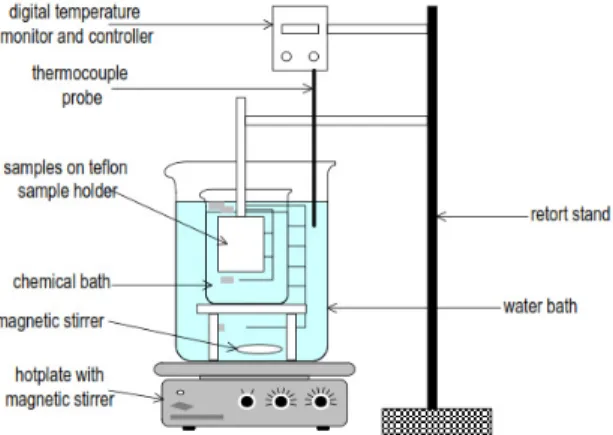
The cadmium sulfide (CdS) thin films were prepared by chemical bath deposition (CBD) method using cadmiumchloride (CdCl2) as a cadmium source (0.1 M), thiourea [SC(NH2)2] as a sulphur source (0.1 M), and ammonia. Fig. 1 shows the schematic of CBD method used in the present study.
Fig. 1. Schematic of chemical bath deposition (CBD) method used in the present study for deposition of CdS films.
The glass substrates were initially clean with soap solution, double distilled water, ethanol, acetone and finally an ultrasonic cleaning for 20 min in double distilled water. Deposition temperature (bath temperature) was varied from 650C to 850C at an interval of 100Cwhile other process parameters being kept constant and are listed in Table 1.
Table 1. Deposition parameters employed for the synthesis of CdS films
Deposition Parameters Values
Cadmium Chloride (CdCl2) 0.1 M
Thiourea [SC(NH2)2] 0.1 M
pH of the bath 11.5
Deposition Time (Minute) 40
Deposition Temperature (0C) 65-85
2.2.Film characterization
Raman spectra were recorded with Raman spectroscopy (Jobin Yvon Horibra LABRAM-HR) in the range 100-1200 cm-1. The spectrometer has backscattering geometry for detection of Raman spectrum with the resolution of 1 cm-1. The excitation source was 532 nm line of He-Ne laser. The power of the Raman laser was kept less than 5 mW to avoid laser induced crystallization on the films. X-ray diffraction pattern were obtained by x-ray diffractometer (Bruker D8 Advance, Germany) using Cu KD line (O = 1.54056 Å). The patterns were taken at a grazing angle of 10. The average crystallite size was estimated using the classical Scherer’sformula [28]. The optical band gap of the CdS films was deduced from transmittance and reflectance spectra of the films deposited on glass and were measured using a JASCO, V-670 UV-Visible spectrophotometer in the range 300-1200 nm. The surface morphology of the films is investigated using scanning electron microscopy (JEOL JSM-6360 A). Thickness of films was determined by profilometer (KLA Tencor, P-16+).
3.Results and Discussion
3.1.Variation in film thickness
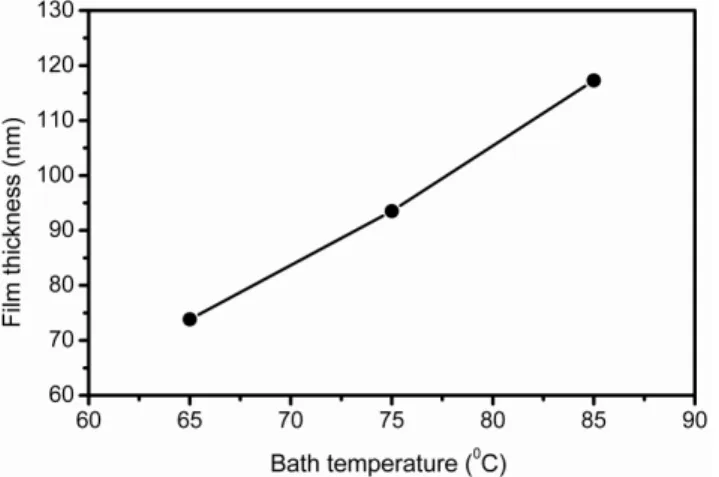
The CdS thin films have been deposited using the chemical bath deposition method and the thickness are measured using electro-mechanical contact Talystep surface profilometer (KLA Tencor, P-16+). The variation of film thickness as a function of bath temperature is shown in Fig. 2.
Fig 2. Thickness variation of CdS thin films deposited at different bath temperatures
As seen from the figure, the film thickness linearly increases with increase in bath temperature. It increases from 73.84 nm to 117.28 nm when the bath temperature increased from 65 0C to 85 0C. It has been reported that too thick CdS films lead to the reduction of photon into the absorber layer, while too thin is hard to synthesize smooth films with few pinholes [29]. However, in the present study we have successfully controlled the CdS film thickness simply by controlling the bath temperature in CBD method.
3.2.Low Angle XRD Analysis
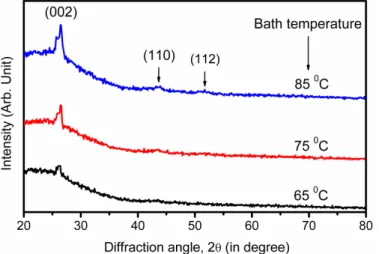
Low angle x-ray diffraction (XRD) is a multipurpose, non-destructive technique which gives direct information about crystallographic structure of materials. Fig. 3 shows the XRD pattern of CdS thin films grown by CBD at different bath temperatures.
Fig. 3.Low angle x-ray diffraction pattern of CdS thin films deposited at different bath temperatures.
As seen from the figure, CdS film deposited at 650C show only a broad peak centered near 2θ = 26.5o which corresponds to (002) plane.. With increase in bath temperature to 75 0C the XRD pattern shows a moderately intense
peak at 2θa 26.50and an additional broad peak centered ~ 2θ = 43.7o which can be assigned (110) planes of the CdS. Finally, the CdS film deposited at 850C, three distinct peaks at 2θa 26.5o, 43.9o and 51.7o corresponding to (002), (110) and (112) planes of CdS can be clearly seen. According to standard JCPDS data card # 41-1049, these peaks correspond to hexagonal CdS [30]. The CdS films deposited at various deposition temperatures clearly shows that these films have (002) preferred orientation of crystallites. This preferred orientation may be due to the controlled nucleation occurring in the film growth process [31].It is therefore concluded that preferred oriented CdS films can be prepared by chemical bath deposition method by controlling the bath temperature. The crystallite size estimated using the classical Debye-Scherer formula is listed In Table 2.It is seen that the crystallite size increases with increase in bath temperature for CBD deposited CdS films.
3.3.Raman Spectroscopy Analysis
Raman spectroscopy is one of the most sensitive tool for information on the local bonding configurations including crystallanity and structure disorders in lattice as well as using this we can understand phase transition [32]. Fig. 4 shows first order Raman spectra of CdS thin films deposited by chemical bath deposition at various bath temperatures. The Raman spectra of CdS thin films prepared at different deposition temperatures represent a well resolved line at 304 cm-1 and 605 cm-1 corresponding to the first order scattering of the longitudinal optical (1 LO) phonon and the second order scattering of longitudinal optical (2 LO) phonon respectively [33, 34]. Similar lines for CdS films were observed by previously by other research groups [35, 36]. A slight and continuous shift of 1LO phonon peak towards higher wave number with increase in bath temperature suggests the improvement of structural order in the film [37]. The ratio of intensity of first order longitudinal optical phonon and the second order longitudinal optical phonon peak, (2LO/1LO) has been often used as an indicator in the evaluation of CdS crystallinity in the film [32].
In the present study, increase in the intensity ratio, 2LO/1LO with increase in bath temperature indicates enhancement of crystallinity of CdS films.
Fig.4. Raman spectra of CdS films deposited at different bath temperatures by chemical bath deposition.
3.4.UV-Visible Spectroscopy Analysis
Fig.5(a) show the UV-Visible transmittance spectra for CdS thin films prepared at different bath temperatures. As seen, all CdS thin films have high transmittance in visible and NIR region of solar spectrum (>70 %). Relatively high transmission of CdS films and sharp fall of transmission at band edge is an indication of low surface roughness and good homogeneity of the film [38]. Transmission in low wavelength region extends up to 300 nm indicate presence of disorders and amorphous components in the film [39]. There are few reports which have reported high transmittance of CdS films at high and low temperatures [40]. However, in present studies, high transmission at lower bath temperature (85 0C) may be due to decrease in voids due to change bath temperature as well as improvement in uniformity, crystallite size and decrease in roughness with increase in deposition temperature.
Fig.5. a) UV-Visible transmission spectra b) Tauc plot for the CdS films prepared at different bath temperature
The absorption coefficient (α) of CdS thin film was calculated from the transmittance spectra using Beer-Lambert approximation using relation [41],
¸ ¹ · ¨ © § T 1 ln α d (1)
Fig. 5(b) shows (αhv)2 versus hv plot (Tauc plot) used to estimate band gap and Table 2 shows the estimated values of band gap from it.
Table 2: Estimated values of crystallite size and band gap at different bath temperatures for CBD deposited CdS films Bath temperature (0C) Crystallite size (nm) Band gap values (nm)
65 16.4 2.89
75 20.3 2.83
85 32.7 2.59
As seen from the graph and Table 2 the optical band gap decreases with increase in bath temperature. Decrease in band gap can attribute to increase in crystallite size with increase in bath temperature. The larger crystallite size leads to an increase in absorption. As a result, the optical absorption edge shift towards longer wavelengths and consequently band gap decreases. Decrease in optical band gap with increase in bath temperature has been reported previously [40].
3.5.Scanning Electron Microscopy (SEM) Analysis
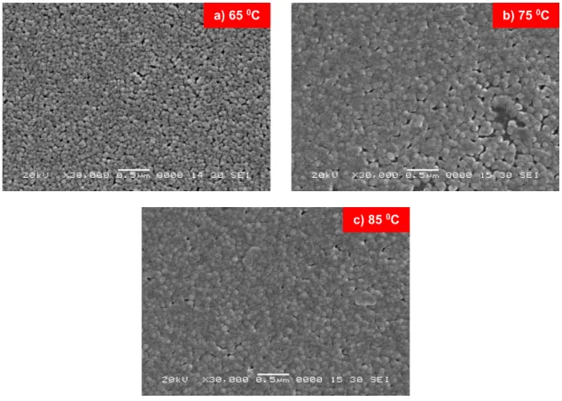
Figure 6 illustrates the scanning electron microscopy (SEM) micrographs of CdS thin films deposited at 650C, 750C and 850C. As seen from the micrographs the surface morphology of all films is much smooth, uniform and crack free. The surface analysis indicates that the morphology of the CdS thin films changes significantly with increasing bath temperature. Small CdS grains are distributed uniformly over the entire substrate surface.
Fig. 6. SEM micrographs of the CdS thin films grown for different bath temperature a) 650C, b) 750C, and c) 850C
a) 65 0C b) 75 0C
The micrographs for the film deposited at 650C show some pinholes and voids. However, with increasing deposition temperature the density of pinholes drastically gets reduced and the film deposited at 850C become dense and almost pinhole free. Furthermore, some particles agglomerated resulting in protrusion can also be seen. Similar results have been reported by X. W. He [29].
4.Conclusions
In the present work, single step synthesis of CdS thin films has been carried out by chemical bath deposition method. The influence of bath temperature on the structural, morphological and optical properties has been investigated systematically. X-ray diffraction (XRD) analysis indicates the formation of crystalline hexagonal phase of CdS with (002) preferred orientation under the prevailing experimental conditions. Raman spectroscopy analysis revealed CdS phase purity. CdS thin films with good adherence have been obtained by CBD onto glass substrates. The SEM analysis showed that CdS thin films are smooth, homogeneous and uniform randomly oriented spherical nanocrystallites. The CdS thin films show high transmission in the range 600-1200 nm with the band gap > 2.6 eV. The bandgap energy values follow an inverse relation with crystallite sizes as expected from quantum sizeeffects. Finally it has been concluded that the CBD grown CdS films can be useful as buffer layer in thin film solar cells.
Acknowledgements
The authors are thankful to the Department of Science and Technology (DST) and Ministry of New and Renewable Energy (MNRE), Government of India and Centre for Nanomaterials and Quantum Systems (CNQS), University of Pune for the financial support. One of the authors Sandesh Jadkar is thankful to University Grants Commission, New Delhi for special financial support under UPE program. Mr. Sachin Rondiya gratefully acknowledges the financial support from Dr. Babasaheb Ambedkar Research & Training Institute (BARTI), Pune, for the award of Junior Research Fellowship.
References
[1] Reynolds DC, Leies G, Antes LL, Marburger RE. Photovoltaic Effect in Cadmium Sulfide. Phys Rev 1954; 96: 533-534.
[2] Jadhav U, Shinde M, Patel S, Patil R. Structural, optical and electrical properties of nanocrystalline cadmium sulphide thin films deposited by
novel chemical route. Indian J Pure Appl Phys 2014; 52: 39Ā43.
[3] Wu CH, Bube RH. Thermoelectric and photothermoelectric effects in semiconductors: Cadmium sulfide films. J Appl Phys 1974; 45: 648-660. [4] Chopra KL, Das SR. Why thin film solar cells?, in: Thin film solar cells. Springer 1983; 1-18.
[5] Al-Douri Y, Waheb JH, Ameri M, Khenata R, Bouhemadou A, Reshak A. Morphology, Analysis and Properties Studies of CdS Nanostructures under Thiourea Concentration Effect for Photovoltaic Applications. Int J Electrochem Sci 2013; 8: 10688-10696.
[6] Apolinar-Iribe A, Acosta-Enriquez M, Quevedo-Lopez M, Ramirez-Bon R, De Leon A, Castillo S. Acetylacetone as complexing agent for CdS thin films grow chemical bath deposition. Chalcogenide Letters 2011; 8: 77-82.
[7] Wacogne B, Roe M, Pattinson T, Pannell CN. Effective piezoelectric activity of zinc oxide films grown by radioǦfrequency planar magnetron sputtering. Appl Phys Lett 1995; 67: 1674-1676.
[8] Stolt L, Hedstrom J, Kessler J, Ruckh M, Velthaus KO, Schock HW. ZnO/CdS/CuInSe2 thinǦfilm solar cells with improved performance. Appl Phys Lett 1993; 62: 597-599.
[9] Keis K, Magnusson E, Lindstrom H, Lindquist SE, Hagfeldt A. A 5% efficient photoelectrochemical solar cell based on nanostructured ZnO electrodes. Sol. Energy Mater. Sol. Cells 2002; 73: 51-58.
[10] Alivisatos AP. Semiconductor clusters, nanocrystals, and quantum dots. Science 1996; 271: 933.
[11] Klein DL, Roth R, Lim AK, Alivisatos AP, McEuen PL. A single-electron transistor made from a cadmium selenide nanocrystal. Nature; 389: 699-701.
[12] Sarma K, Bordolo RK, Sarma M & Gangurly JN. J Instrum Soc India 2001; 31: 216.
[13] Cao G, Liu D. Template-based synthesis of nanorod, nanowire, and nanotube arrays. Adv in colloid interface sci 2008; 136: 45-64. [14] Senthil K, Mangalaraj D, Narayandass SK. Structural and optical properties of CdS thin films. Appl sur sci 2001; 169: 476-479.
[15] Perna G, Capozzi V, Ambrico M, Augelli V, Ligonzo T, Minafra A, Schiavulli L, Pallara M. Structural and optical characterization of undoped and indium-doped CdS films grown by pulsed laser deposition. Thin Solid Films 2004; 453: 187-194.
[17] Ikhmayies SJ. Production and characterization of CdS/CdTe thin film photovoltaic solar cells of potential industrial use, Amman: University of Jordan 2002.
[18] Trajic J, Gilic M, Romcevic N, Romcevic M, Stanisic G, Hadzic B, Petrovic M, Yahia Y. Raman Spectroscopy of Optical Properties In CdS Thin Films. Science of Sintering 2015; 47: 145.
[19] Canevari V, Romeo N, Sberveglieri G, Azzi S, Tosi A, Curti M, Zanotti L. Low resistivity CdS thin films grown by flashǦevaporation at low substrate temperature (150–200° C). Journal of Vacuum Science & Technology A, 1984; 2: 9-10.
[20] Shay JL, Wagner S, Bettini M, Bachmann KJ, Buehler E. InP—CdS solar cells, IEEE Transactions on Electron Devices. 1977; 24: 483-486. [21] Piel A, Murray H. Etude de la conduction Poole-Frenkel dissymétrique dans des structures Al-CdS-Au. Thin Solid Films 1977; 44: 65-73. [22] Croitoru N, Jakobson S. Properties of CdS films and Cu 2 S-CdS junctions prepared by chemical printing. Thin Solid Films 1979; 56: L5-L7. [23] Khan TM, BiBi T. Application of NS Pulsed Laser Ablation for Dense CdS Nanoparticles Deposition in Argon Atmosphere.
[24] Zhang Y, Ma H, Wu D, Li R, Wang X, Wang Y, Zhu W, Wei Q, Du B. A generalized in situ electrodeposition of Zn doped CdS-based photoelectrochemical strategy for the detection of two metal ions on the same sensing platform. Biosensors and Bioelectronics 2016; 77: 936-941.
[25] Kim W, Baek M, Yong K. Fabrication of ZnO/CdS, ZnO/CdO core/shell nanorod arrays and investigation of their ethanol gas sensing properties. Sensors and Actuators B: Chemical 2016; 223: 599-605.
[26] Wilson K, Ahamed MB. Surface modification of cadmium sulfide thin film honey comb nanostructures: Effect of in situ tin doping using chemical bath deposition. Appl surf sci 2016; 361: 277-282.
[27] Yılmaz S, Atasoy Y, Tomakin M, Bacaksız E. Comparative studies of CdS, CdS: Al, CdS: Na and CdS:(Al–Na) thin films prepared by spray pyrolysis. Superlattices and Microstructures 2015; 88: 299-307.
[28] Cullity B, Stock S. Elementary of X-ray Diffraction, Englewood Cliffs, 3rd, 2001.
[29] He XW, Liu WF, Zhu CF, Jiang GS. CdS thin films deposited by CBD method on glass. Chin J Chem Phys 2011; 24: 471-476.
[30] Bansal N, Reynolds LX, MacLachlan A, Lutz T, Ashraf RS, Zhang W, Nielsen CB, McCulloch I, Rebois DG, Kirchartz T. Influence of crystallinity and energetics on charge separation in polymer–inorganic nanocomposite films for solar cells. Scientific reports 2013; 3 . [31] Sasikala G, Thilakan P, Subramanian C. Modification in the chemical bath deposition apparatus, growth and characterization of CdS
semiconducting thin films for photovoltaic applications, Sol. Energy Mater. Sol. Cells 2000; 62: 275-293.
[32] Kwon JH, Ahn JS, Yang H. Chemical bath deposition of CdS channel layer for fabrication of low temperature-processed thin-film-transistors. Curr Appl Phys 2013; 13: 84-89.
[33] Trujillo O, Moss R, Vuong K, Lee D, Noble R, Finnigan D, Orloff S, Tenpas E, Park C, Fagan J. CdS thin film deposition by CW Nd: YAG laser. Thin Solid Films 1996; 290: 13-17.
[34] Lee J. Raman scattering and photoluminescence analysis of B-doped CdS thin films. Thin Solid Films 2004; 451: 170-174. [35] Leite R, Porto S. Enhancement of Raman cross section in CdS due to resonant absorption. Phys Rev Lett 1966; 17: 10.
[36] Chuu D, Dai C, Hsieh W, Tsai C. Raman investigations of the surface modes of the crystallites in CdS thin films grown by pulsed laser and thermal evaporation. J Appl Phys 1991; 69: 8402-8404.
[37] Oladeji I, Chow L, Liu J, Chu W, Bustamante A, Fredricksen C, Schulte A. Comparative study of CdS thin films deposited by single, continuous, and multiple dip chemical processes. Thin Solid Films 2000; 359: 154-159.
[38] Lee JH, Song WC, Yi JS, Yang KJ, Han WD, Hwang J. Growth and properties of the Cd 1− x Zn x S thin films for solar cell applications.
Thin Solid Films 2003; 431: 349-353.
[39] Liu F, Lai Y, Liu J, Wang B, Kuang S, Zhang Z, Li J, Liu Y. Characterization of chemical bath deposited CdS thin films at different deposition temperature. J Alloys Compd 2010; 493: 305-308.
[40] Kumar S, Sharma P, Sharma V. CdS nanofilms: effect of deposition temperature on morphology and optical band gap. Physica Scripta 2013; 88: 045603[41] J. J Tauc: Amorphous and Liquid Semiconductor, Plenum, New York: (1976)