[Guide Subtitle]
[optional]
UG761 (v13.1) March 7, 2011 [optional]
Guide
XILINX EXPRESSLY DISCLAIMS ANY WARRANTY WHATSOEVER WITH RESPECT TO THE ADEQUACY OF THE INFORMATION OR ANY IMPLEMENTATION BASED THEREON, INCLUDING BUT NOT LIMITED TO ANY WARRANTIES OR REPRESENTATIONS THAT THIS IMPLEMENTATION IS FREE FROM CLAIMS OF INFRINGEMENT AND ANY IMPLIED WARRANTIES OF MERCHANTABILITY OR FITNESS FOR A PARTICULAR PURPOSE.
Except as stated herein, none of the Information may be copied, reproduced, distributed, republished, downloaded, displayed, posted, or transmitted in any form or by any means including, but not limited to, electronic, mechanical, photocopying, recording, or otherwise, without the prior written consent of Xilinx.
© 2011 Xilinx, Inc. XILINX, the Xilinx logo, Virtex, Spartan, ISE, and other designated brands included herein are trademarks of Xilinx in the United States and other countries. All other trademarks are the property of their respective owners.
ARM® and AMBA® are registered trademarks of ARM in the EU and other countries. All other trademarks are the property of their respective owners.
Revision History
The following table shows the revision history for this document:
Date Version Description of Revisions
09/21/2010 1.0 Initial Xilinx release in 12.4. 03/01/2011 2.0 Second Xilinx release in 13.1.
Added new AXI Interconnect features.
Corrected ARESETN descriptionin Appendix A. 03/07/2011 3.0 Corrected broken link.
Revision History . . . 2
Chapter 1: Introducing AXI for Xilinx System Development
Introduction
. . . 5What is AXI?
. . . . 5Summary of AXI4 Benefits . . . 6
How AXI Works
. . . 6IP Interoperability
. . . 8About Data Interpretation . . . 8
About IP Compatibility . . . 8
Infrastructure IP . . . 9
Memory Mapped Protocols . . . 9
AXI4-Stream Protocol . . . 9
Combining AXI4-Stream and Memory Mapped Protocols . . . 9
What AXI Protocols Replace
. . . 10Targeted Reference Designs
. . . 10Additional References. . . 10
Chapter 2: AXI Support in Xilinx Tools and IP
AXI Development Support in Xilinx Design Tools
. . . 13Using Embedded Development Kit: Embedded and System Edition . . . 13
Creating an Initial AXI Embedded System. . . 13
Creating and Importing AXI IP. . . 13
Debugging and Verifying Designs: Using ChipScope in XPS. . . 14
Using Processor-less Embedded IP in Project Navigator . . . 14
Using System Generator: DSP Edition . . . 14
AXI4 Support in System Generator. . . 14
Using Xilinx AXI IP: Logic Edition . . . 17
Xilinx AXI Infrastructure IP
. . . 18Xilinx AXI Interconnect Core IP . . . 19
AXI Interconnect Core Features . . . 19
AXI Interconnect Core Limitations. . . 21
AXI Interconnect Core Diagrams . . . 22
AXI Interconnect Core Use Models. . . 22
Width Conversion. . . 26
N-to-M Interconnect (Shared Access Mode). . . 27
Clock Conversion . . . 28
Pipelining . . . 28
Peripheral Register Slices . . . 29
Data Path FIFOs . . . 29
Connecting AXI Interconnect Core Slaves and Masters. . . 29
AXI-To-AXI Connector Features. . . 29
Description . . . 29
Using the AXI To AXI Connector . . . 30
AXI Centralized DMA Scatter Gather Feature . . . 33
Centralized DMA Configurable Features. . . 33
Centralized DMA AXI4 Interfaces . . . 34
Ethernet DMA . . . 34
AXI4 DMA Summary. . . 36
DMA AXI4 Interfaces . . . 37
Video DMA . . . 38
AXI VDMA Summary. . . 39
VDMA AXI4 Interfaces. . . 40
Memory Control IP and the Memory Interface Generator . . . 40
Virtex-6. . . 41
Spartan-6 Memory Control Block. . . 41
Chapter 3: AXI Feature Adoption in Xilinx FPGAs
Memory Mapped IP Feature Adoption and Support. . . 43
AXI4-Stream Adoption and Support
. . . 45AXI4-Stream Signals . . . 45
Numerical Data in an AXI4-Stream . . . 45
Real Scalar Data Example. . . 47
Complex Scalar Data Example . . . 48
Vector Data Example . . . 49
Packets and NULL Bytes . . . 52
Sideband Signals. . . 53
Events. . . 53
TLAST Events. . . 54
DSP and Wireless IP: AXI Feature Adoption
. . . 55Chapter 4: Migrating to Xilinx AXI Protocols
Introduction
. . . 57Migrating to AXI for IP Cores . . . 57
The AXI To PLB Bridge
. . . 58Features . . . 58
AXI4 Slave Interface . . . 58
PLBv4.6 Master Interface . . . 59
AXI to PLBv4.6 Bridge Functional Description . . . 59
Migrating Local-Link to AXI4-Stream. . . 60
Required Local-Link Signal to AXI4-Stream Signal Mapping . . . 60
Optional Local-Link Signal to AXI4-Stream Signal Mapping. . . 62
Variations in Local-Link IP. . . 63
Local-Link References. . . 63
Using System Generator for Migrating IP. . . 63
Migrating a System Generator for DSP IP to AXI . . . 63
Resets . . . 63
Clock Enables . . . 63
TDATA. . . 63
Port Ordering . . . 64
Latency. . . 65
Slave FSL to AXI4-Stream Signal Mapping . . . 66
Differences in Throttling . . . 66
Migrating HDL Designs to use DSP IP with AXI4-Stream
. . . 67DSP IP-Specific Migration Instructions . . . 67
Demonstration Testbench. . . 67
Using CORE Generator to Upgrade IP . . . 68
Latency Changes . . . 68
Slave FSL to AXI4-Stream Signal Mapping . . . 69
Software Tool Considerations for AXI Migration (Endian Swap)
. . . 69Guidelines for Migrating Big-to-Little Endian . . . 70
Data Types and Endianness
. . . 71High End Verification Solutions. . . 72
Appendix A: AXI Adoption Summary
AXI4 and AXI4-Lite Signals
. . . 73Global Signals . . . 73
AXI4 and AXI4-Lite Write Address Channel Signals . . . 73
AXI4 and AXI4-Lite Write Data Channel Signals . . . 74
AXI4 and AXI4-Lite Write Response Channel Signals . . . 75
AXI4 and AXI4-Lite Read Address Channel Signals . . . 75
AXI4 and AXI4-Lite Read Data Channel Signals . . . 76
AXI4-Stream Signal Summary
. . . 77Introducing AXI for Xilinx System Development
Introduction
Xilinx® has adopted the Advanced eXtensible Interface (AXI) protocol for Intellectual
Property (IP) cores beginning with the Spartan®-6 and Virtex®-6 devices. This document is intended to:
• Introduce key concepts of the AXI protocol
• Give an overview of what Xilinx tools you can use to create AXI-based IP • Explain what features of AXI Xilinxhas adopted
• Provide guidance on how to migrate your existing design to AXI
Note: This document is not intended to replace the Advanced Microcontroller Bus
Architecture (AMBA®) ARM® AXI4 specifications. Before beginning an AXI design, you need to download, read, and understand the ARM AMBA AXI Protocol v2.0 Specification, along with the
AMBA4 AXI4-Stream Protocol v1.0.
These are the steps to download the specifications; you might need to fill out a brief registration before downloading the documents:
1. Go to www.amba.com
2. Click Download Specifications.
3. In the Contents pane on the left, click AMBA > AMBA Specifications >AMBA4. 4. Download both the ABMA AXI4-Stream Protocol Specification and AMBA AXI Protocol
Specification v2.0.
What is AXI?
AXI is part of ARM AMBA, a family of micro controller buses first introduced in 1996. The first version of AXI was first included in AMBA 3.0, released in 2003. AMBA 4.0, released in 2010, includes the second version of AXI, AXI4.
There are three types of AXI4 interfaces:
• AXI4—for high-performance memory-mapped requirements.
• AXI4-Lite—for simple, low-throughput memory-mapped communication (for example, to and from control and status registers).
• AXI4-Stream—for high-speed streaming data.
Summary of AXI4 Benefits
AXI4 provides improvements and enhancements to the Xilinx product offering across the board, providing benefits to Productivity, Flexibility, and Availability:
• Productivity—By standardizing on the AXI interface, developers need to learn only a single protocol for IP.
• Flexibility—Providing the right protocol for the application:
• AXI4 is for memory mapped interfaces and allows burst of up to 256 data transfer cycles with just a single address phase.
• AXI4-Lite is a light-weight, single transaction memory mapped interface. It has a small logic footprint and is a simple interface to work with both in design and usage.
• AXI4-Stream removes the requirement for an address phase altogether and allows unlimited data burst size. AXI4-Stream interfaces and transfers do not have address phases and are therefore not considered to be memory-mapped. • Availability—By moving to an industry-standard, you have access not only to the
Xilinx IP catalog, but also to a worldwide community of ARM Partners. • Many IP providers support the AXI protocol.
• A robust collection of third-party AXI tool vendors is available that provide a variety of verification, system development, and performance characterization tools. As you begin developing higher performance AXI-based systems, the availability of these tools is essential.
How AXI Works
This section provides a brief overview of how the AXI interface works. The Introduction, page 5, provides the procedure for obtaining the ARM specification. Consult those specifications for the complete details on AXI operation.
The AXI specifications describe an interface between a single AXI master and a single AXI slave, representing IP cores that exchange information with each other. Memory mapped AXI masters and slaves can be connected together using a structure called an Interconnect
block. The Xilinx AXI Interconnect IP contains AXI-compliant master and slave interfaces, and can be used to route transactions between one or more AXI masters and slaves. The AXI Interconnect IP is described in Xilinx AXI Interconnect Core IP, page 19.
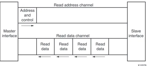
Both AXI4 and AXI4-Lite interfaces consist of five different channels: • Read Address Channel
• Write Address Channel • Read Data Channel • Write Data Channel • Write Response Channel
Data can move in both directions between the master and slave simultaneously, and data transfer sizes can vary. The limit in AXI4 is a burst transaction of up to 256 data transfers. AXI4-Lite allows only 1 data transfer per transaction.
Figure 1-1, page 7 shows how an AXI4 Read transaction uses the Read address and Read data channels:
Figure 1-2 shows how a Write transaction uses the Write address, Write data, and Write response channels.
As shown in the preceding figures, AXI4 provides separate data and address connections for Reads and Writes, which allows simultaneous, bidirectional data transfer. AXI4 requires a single address and then bursts up to 256 words of data. The AXI4 protocol describes a variety of options that allow AXI4-compliant systems to achieve very high data throughput. Some of these features, in addition to bursting, are: data upsizing and downsizing, multiple outstanding addresses, and out-of-order transaction processing. At a hardware level, AXI4 allows a different clock for each AXI master-slave pair. In addition, the AXI protocol allows the insertion of register slices (often called pipeline stages) to aid in timing closure.
Figure 1-1: Channel Architecture of Reads
Figure 1-2: Channel Architecture of Writes
Master interface Read address channel Address and control Read data channel Read data Read data Read data Read data Slave interface X12076 Master interface
Write address channel Address and control Write data channel Write data Write data Write data Write data Write response Write response channel
Slave interface
AXI4-Lite is similar to AXI4 with some exceptions, the most notable of which is that bursting, is not supported. The AXI4-Lite chapter of the ARM AMBA AXI Protocol v2.0 Specification describes the AXI4-Lite protocol in more detail.
The AXI4-Stream protocol defines a single channel for transmission of streaming data. The AXI4-Stream channel is modeled after the Write Data channel of the AXI4. Unlike AXI4, AXI4-Stream interfaces can burst an unlimited amount of data. There are additional, optional capabilities described in the AXI4-Stream Protocol Specification. The specification describes how AXI4-Stream-compliant interfaces can be split, merged, interleaved, upsized, and downsized. Unlike AXI4, AXI4-Stream transfers cannot be reordered. With regards to AXI4-Stream, it should be noted that even if two pieces of IP are designed in accordance with the AXI4-Stream specification, and are compatible at a signaling level, it does not guarantee that two components will function correctly together due to higher level system considerations. Refer to the AXI IP specifications at
http://www.xilinx.com/ipcenter/axi4.htm, and AXI4-Stream Signals, page 45 for more information.
IP Interoperability
The AXI specification provides a framework that defines protocols for moving data between IP using a defined signaling standard. This standard ensures that IP can exchange data with each other and that data can be moved across a system.
AXI IP interoperability affects: • The IP application space • How the IP interprets data
• Which AXI interface protocol is used (AXI4, AXI4-Lite, or AXI4-Stream)
The AXI protocol defines how data is exchanged, transferred, and transformed. The AXI protocol also ensures an efficient, flexible, and predictable means for transferring data.
About Data Interpretation
The AXI protocol does not specify or enforce the interpretation of data; therefore, the data contents must be understood, and the different IP must have a compatible interpretation of the data.
For IP such as a general purpose processor with an AXI4 memory mapped interface, there is a great degree of flexibility in how to program a processor to format and interpret data as required by the Endpoint IP.
About IP Compatibility
For more application-specific IP, like an Ethernet MAC (EMAC) or a video display IP using AXI4-Stream, the compatibility of the IP is more limited to their respective application spaces. For example, directly connecting an Ethernet MAC to the video display IP would not be feasible.
Note: Even though two IP such as EMAC and Video Streaming can theoretically exchange data with each other, they would not function together because the two IP interpret bit fields and data packets in a completely different manner.
Infrastructure IP
An infrastructure IP is another IP form used to build systems. Infrastructure IP tends to be a generic IP that moves or transforms data around the system using general-purpose AXI4 interfaces and does not interpret data.
Examples of infrastructure IP are: • Register slices (for pipeling)
• AXI FIFOs (for buffering/clock conversion)
• AXI Interconnect IP (connects memory mapped IP together)
• AXI Direct Memory Access (DMA) engines (memory mapped to stream conversion) These IP are useful for connecting a number of IP together into a system, but are not generally endpoints for data.
Memory Mapped Protocols
In memory mapped AXI (AXI3, AXI4, and AXI4-Lite), all transactions involve the concept of a target address within a system memory space and data to be transferred.
Memory mapped systems often provide a more homogeneous way to view the system, because the IPs operate around a defined memory map.
AXI4-Stream Protocol
The AXI4-Stream protocol is used for applications that typically focus on a data-centric and data-flow paradigm where the concept of an address is not present or not required. Each AXI4-Stream acts as a single unidirectional channel for a handshake data flow. At this lower level of operation (compared to the memory mapped AXI protocol types), the mechanism to move data between IP is defined and efficient, but there is no unifying address context between IP. The AXI4-Stream IP can be better optimized for performance in data flow applications, but also tends to be more specialized around a given application space.
Combining AXI4-Stream and Memory Mapped Protocols
Another approach is to build systems that combine AXI4-Stream and AXI memory mapped IP together. Often a DMA engine can be used to move streams in and out of memory. For example, a processor can work with DMA engines to decode packets or implement a protocol stack on top of the streaming data to build more complex systems where data moves between different application spaces or different IP.
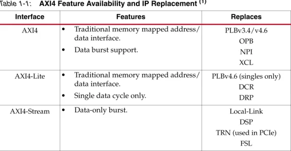
What AXI Protocols Replace
Table 1-1 lists the high-level list of AXI4 features available and what protocols an AXI option replaces.
Targeted Reference Designs
The other chapters of this document go into more detail about AXI support in Xilinx tools and IP. To assist in the AXI transition, the Spartan-6 and Virtex-6 Targeted Reference Designs, which form the basis of the Xilinx targeted domain platform solution, have been migrated to support AXI. These targeted reference designs provide the ability to
investigate AXI usage in the various Xilinx design domains such as Embedded, DSP, and Connectivity. More information on the targeted reference designs is available at
http://www.xilinx.com/products/targeted_design_platforms.htm.
Additional References
Additional reference documentation:
• ARM AMBA AXI Protocol v2.0 Specification • AMBA4 AXI4-Stream Protocol v1.0
See the Introduction, page 5 for instructions on how to download the ARM® AMBA® AXI specification from http://www.amba.com.
Additionally, this document references the following documents, located at the following Xilinx website:
http://www.xilinx.com/support/documentation/axi_ip_documentation.htm.
• AXII Interconnect IP (DS768)
• AXI-To-AXI Connector IP Data Sheet (DS803) • AXI External Master Connector (DS804) • AXI External Slave Connector (DS805)
• MicroBlaze Processor Reference Guide (UG081)
Table 1-1: AXI4 Feature Availability and IP Replacement (1)
Interface Features Replaces
AXI4 • Traditional memory mapped address/ data interface.
• Data burst support.
PLBv3.4/v4.6 OPB NPI XCL AXI4-Lite • Traditional memory mapped address/
data interface.
• Single data cycle only.
PLBv4.6 (singles only) DCR
DRP AXI4-Stream • Data-only burst. Local-Link
DSP TRN (used in PCIe)
FSL 1. See Chapter 4, “Migrating to Xilinx AXI Protocols,” for more information.
This document lists the following Xilinx websites:
• AXI IP document website: http://www.xilinx.com/ipcenter/axi4.htm • EDK website: http://www.xilinx.com/tools/embedded.htm
• CORE Generator® tool: http://www.xilinx.com/tools/coregen.htm
• Memory Control: http://www.xilinx.com/products/design_resources/mem_corner • System Generator: http://www.xilinx.com/tools/sysgen.htm
• Local-Link:
http://www.xilinx.com/products/design_resources/conn_central/locallink_member/sp06.pdf • Targeted Designs: http://www.xilinx.com/products/targeted_design_platforms.htm • Answer Record: http://www.xilinx.com/support/answers/37425.htm
AXI Support in Xilinx Tools and IP
AXI Development Support in Xilinx Design Tools
This section describes how Xilinx® tools can be used to build systems of interconnected Xilinx AXI IP (using Xilinx Platform Studio or System Generator for DSP), and deploy individual pieces of AXI IP (using the CORE Generator™ tool).
Using Embedded Development Kit: Embedded and System Edition
Xilinx ISE Design Suite: Embedded Edition and System Editionsupport the addition of AXI cores into your design through the tools described in the following subsections.
Creating an Initial AXI Embedded System
The following Embedded Development Kit (EDK) tools support the creation and addition of AXI-based IP Cores (pcores).
• Base System Builder (BSB) wizard—creates either AXI or PLBv.46 working embedded designs using any features of a supported development board or using basic functionality common to most embedded systems. After creating a basic system, customization can occur in the main Xilinx Platform Studio (XPS) view and ISE. Xilinx recommends using the BSB to start new designs. Refer to the XPS Help for more information.
• Xilinx Platform Studio (XPS)—provides a block-based system assembly tool for connecting blocks of IPs together using many bus interfaces (including AXI) to create embedded systems, with or without processors. XPS provides a graphical interface for connection of processors, peripherals, and bus interfaces.
• Software Development Toolkit (SDK)— is the software development environment for application projects. SDK is built with the Eclipse open source standard. For AXI-based embedded systems, hardware platform specifications are exported in an XML format to SDK (XPS-based software development and debugging is not supported.) Refer to SDK Help for more information.
More information on EDK is available at:
http://www.xilinx.com/support/documentation/dt_edk.htm.
Creating and Importing AXI IP
XPS contains a Create and Import Peripheral (CIP) wizard that automates adding your IP to the IP repository in Platform Studio.
Debugging and Verifying Designs: Using ChipScope in XPS
The ChipScope™ Pro Analyzer AXI monitor core, chipscope_axi_monitor, aids in
monitoring and debugging Xilinx AXI4 or AXI4-Lite protocol interfaces. This core lets you probe any AXI, memory mapped master or slave bus interface. It is available in XPS. With this probe you can observe the AXI signals going from the peripheral to the AXI Interconnect core. For example, you can set a monitor on a MicroBlaze processor instruction or data interface to observe all memory transactions going in and out of the processor.
Each monitor core works independently, and allows chaining of trigger outputs to enable taking system level measurements. By using the auxiliary trigger input port and the trigger output of a monitor core you can create multi-level triggering environments to simplify complex system-level measurements.
For example, if you have a master operating at 100MHz and a slave operating at 50MHz, this multi-tiered triggering lets you analyze the transfer of data going from one time domain to the next. Also, with this system-level measurement, you can debug complex multi-time domain system-level issues, and analyze latency bottlenecks in your system. You can add the chipscope_axi_monitor core to your system using the IP Catalog in XPS available under the /debug folder as follows:
1. Put the chipscope_axi_monitor into your bus interface System Assembly View (SAV). 2. Select the bus you want to probe from the Bus Name field.
After you select the bus, an “M” for monitor displays between your peripheral and the AXI Interconnect core IP.
3. Add a ChipScope ICON core to your system, and connect the control bus to the AXI monitor.
4. In the SAV Ports tab, on the monitor core, set up the MON_AXI_ACLK port of the core to match the clock used by the AXI interface being probed.
Optionally, you can assign the MON_AXI_TRIG_OUT port and connect it to other chipscope_axi_monitor cores in the system.
Using Processor-less Embedded IP in Project Navigator
You might want to use portions of EDK IP outside of a processor system. For example, you can use an AXI Interconnect core block to create a multiported DDR3 controller. XPS can be used to manage, connect, and deliver EDK IP, even without a processor. See Xilinx Answer Record 37856 for more information.
Using System Generator: DSP Edition
System Generator for DSP supports both AXI4 and AXI4-Stream interfaces: • AXI4 interface is supported in conjunction with the EDK Processor Block.
• AXI4-Stream interface is supported in IPs found in the System Generator AXI4 block library.
AXI4 Support in System Generator
AXI4 (memory-mapped) support in System Generator is available through the EDK Processor block found in the System Generator block set. The EDK Processor block lets you
connect hardware circuits created in System Generator to a Xilinx MicroBlaze™ processor; options to connect to the processor using either a PLBv4.6 or an AXI4 interface are available.
You do not need to be familiar with the AXI4 nomenclature when using the System Generator flow because the EDK Processor block provides an interface that is memory-centric and works with multiple bus types.
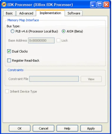
You can create hardware that uses shared registers, shared FIFOs, and shared memories, and the EDK Processor block manages the memory connection to the specified interface. Figure 2-1 shows the EDK Processor Implementation tab with an AXI4 bus type selected.
Port Name Truncation
System Generator shortens the AXI4-Stream signal names to improve readability on the block; this is cosmetic and the complete AXI4-Stream name is used in the netlist. The name truncation is turned on by default; uncheck the Display shortened port names option in the block parameter dialog box to see the full name.
Port Groupings
System Generator groups together and color-codes blocks of AXI4-Stream channel signals. In the example illustrated in the following figure, the top-most input port, data_tready, and the top two output ports, data_tvalid and data_tdata belong in the same AXI4-Stream channel, as well as phase_tready, phase_tvalid, and phase_tdata.
System Generator gives signals that are not part of any AXI4-Stream channels the same background color as the block; the rst signal, shown in Figure 2-2, is such an example.
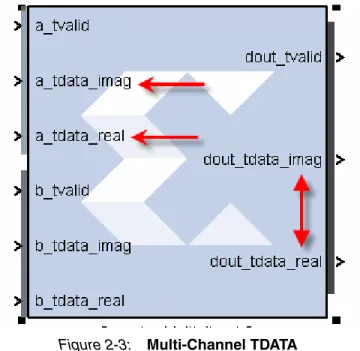
Breaking Out Multi-Channel TDATA
The TDATA signal in an AXI4-Stream can contain multiple channels of data. In System Generator, the individual channels for TDATA are broken out; for example, in the complex multiplier shown in Figure 2-3 the TDATA for the dout port contains both the imaginary and the real number components.
Note: Breaking out of multi-channel TDATA does not add additional logic to the design. The data is correctly byte-aligned also.
For more information about System Generator and AXI IP creation, see the following Xilinx website: http://www.xilinx.com/tools/sysgen.htm.
Figure 2-2: Block Signal Groupings
Using Xilinx AXI IP: Logic Edition
Xilinx IP with an AXI4 interface can be accessed directly from the IP catalog in CORE Generator, Project Navigator, and PlanAhead. An AXI4 column in the IP catalog shows IP with AXI4 support. The IP information panel displays the supported AXI4, AXI4-Stream, and AXI4-Lite interface.
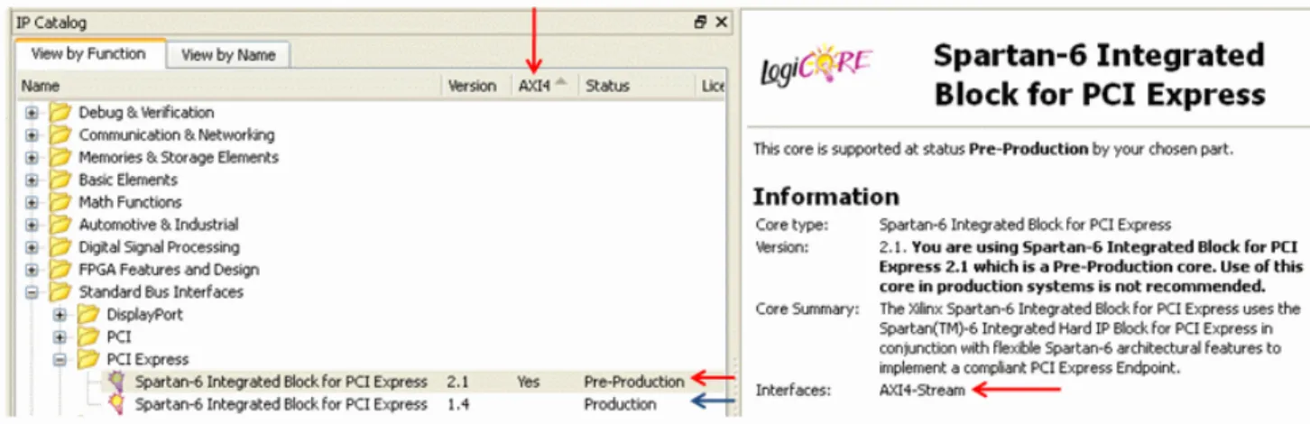
Generally, for Virtex®-6 and Spartan®-6 device families, the AXI4 interface is supported by the latest version of an IP. Older, “Production,” versions of IP continue to be supported by the legacy interface for the respective core on Virtex-6, Spartan-6, Virtex®-5, Virtex®-4 and Spartan®-3 device families. The IP catalog displays all “Production” versions of IP by default. Figure 2-4 shows the IP Catalog in CORE Generator.
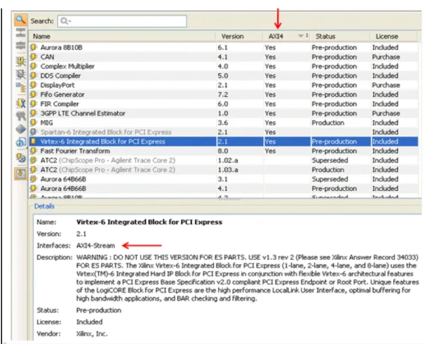
Figure 2-5, page 18 shows the IP catalog in PlanAhead with the equivalent AXI4 column and the supported AXI4 interfaces in the IP details panel.
Xilinx AXI Infrastructure IP
Xilinx has migrated a significant portion of the available IP to AXI prototol. This section provides an overview of the more complex IP that will be used in many AXI-based systems.
The following common infrastructure Xilinx IP is available for Virtex®-6 and Spartan®-6 devices, and future device support:
• Xilinx AXI Interconnect Core IP
• Connecting AXI Interconnect Core Slaves and Masters • External Masters and Slaves
• Centralized DMA • Ethernet DMA • Video DMA
• Memory Control IP and the Memory Interface Generator
Refer to Chapter 4, “Migrating to Xilinx AXI Protocols,” for more detailed usage information. See the following for a list of all AXI IP:
http://www.xilinx.com/ipcenter/axi4.htm.
Xilinx AXI Interconnect Core IP
The AXI Interconnect core IP (axi_interconnect) connects one or more AXI
memory-mapped master devices to one or more memory-mapped slave devices. The AXI interfaces conform to the AMBA® AXI version 4 specification from ARM®, including the AXI4-Lite control register interface subset.
Note: The AXI Interconnect core IP is intended for memory-mapped transfers only; AXI4-Stream transfers are not applicable. IP with AXI4-Stream interfaces are generally connected to one another, and to DMA IP.
The AXI Interconnect core IP is provided as an encrypted, non-licensed (free) pcore in the Xilinx Platform Studio software.
AXI Interconnect Core Features
The AXI Interconnect IP contains the following features:
• AXI protocol compliant (AXI3, AXI4, and AXI4-Lite), which includes: • Burst lengths up to 256 for incremental (INCR) bursts
• Converts AXI4 bursts >16 beats when targeting AXI3 slaves by splitting transactions.
• Generates REGION outputs for slaves with multiple address decode ranges • Propagates USER signals on each channel, if any; independent USER signal width
per channel (optional)
• Propagates Quality of Service (QoS) signals, if any; not used by the AXI Interconnect core(optional)
• Interface data widths:
• AXI4: 32, 64, 128, or 256 bits. • AXI4-Lite: 32 bits
• 32-bit address width
• Connects 1-16 masters to 1-16 slaves:
• When connecting one master to one slave, the AXI Interconnect core can optionally perform address range checking. Also, it can perform any of the normal data-width, clock-rate, or protocol conversions and pipelining.
• When connecting one master to one slave and not performing any conversions or address range checking, the AXI Interconnect core is implemented as wires, with no resources, no delay and no latency.
• Built-in data-width conversion:
• Each master and slave connection can independently use data widths of 32, 64, 128, or 256 bits wide:
- The internal crossbar can be configured to have a native data-width of 32, 64, 128, or 256 bits.
- Data-width conversion is performed for each master and slave connection that does not match the crossbar native data-width.
• When converting to a wider interface (upsizing), data is packed (merged) optionally, when permitted by address channel control signals (CACHE modifiable bit is asserted).
• When converting to a narrower interface (downsizing), burst transactions can be split into multiple transactions if the maximum burst length would otherwise be exceeded.
• Built-in clock-rate conversion:
• Each master and slave connection can use independent clock rates
• Synchronous integer-ratio (N:1 and 1:N) conversion to the internal crossbar native clock-rate.
• Asynchronous clock conversion (uses more storage and incurs more latency than synchronous conversion).
• The AXI Interconnect core exports reset signals re-synchronized to the clock rate of each connected master and slave.
• Built-in AXI4-Lite protocol conversion:
• The AXI Interconnect core can connect to any mixture of AXI4 and AXI4-Lite masters and slaves.
• The AXI Interconnect core saves transaction IDs and restores them during response transfers, when connected to an AXI4-Lite slave.
- AXI4-Lite slaves do not need to sample or store IDs.
• The AXI Interconnect core detects illegal AXI4-Lite transactions from AXI4 masters, such as any transaction that results in a burst of more than one word. It generates a protocol-compliant error response to the master, and does not propagate the illegal transaction to the AXI4-Lite slave.
• Write and Read transactions are single-threaded to AXI4-Lite slaves, propagating only a single address at a time, which typically nullifies the resource overhead of separate write and read address signals.
• Built-in AXI3 protocol conversion:
• The AXI Interconnect core splits burst transactions of more than 16 beats from AXI4 masters into multiple transactions of no more than 16 beats when connected to an AXI3 slave.
• Optional register-slice pipelining:
• Available on each AXI channel connecting to each master and each slave. • Facilitates timing closure by trading-off frequency vs. latency.
• One latency cycle per register-slice, with no loss in data throughput under all AXI handshaking conditions.
• Optional data-path FIFO buffering:
• Available on Write and Read datapaths connecting to each master and each slave. • 32-deep LUT-RAM based.
• 512-deep block RAM based. • Selectable Interconnect Architecture:
• Shared-Address, Multiple-Data (SAMD) crossbar:
- Parallel crossbar pathways for Write data and Read data channels. When more than one Write or Read data source has data to send to different destinations, data transfers may occur independently and concurrently, provided AXI ordering rules are met.
- Sparse crossbar data pathways according to configured connectivity map, resulting in reduced resource utilization.
- One shared Write address arbiter, plus one shared Read address arbiter. Arbitration latencies typically do not impact data throughput when transactions average at least three data beats.
• Shared Access mode (Area optimized):
- Shared write data, shared read data, and single shared address pathways.
- Issues one outstanding transaction at a time.
- Minimizes resource utilization. • Supports multiple outstanding transactions:
• Supports masters with multiple reordering depth (ID threads). • Supports up to 16-bit wide ID signals (system-wide).
• Supports Write response re-ordering. Read data re-ordering, and Read Data interleaving.
• Configurable Write and Read transaction acceptance limits for each connected master.
• Configurable Write and Read transaction issuing limits for each connected slave. • “Single-Slave per ID” method of cyclic dependency (deadlock) avoidance:
• For each ID thread issued by a connected master, the master can have outstanding transactions to only one slave for Writes and one slave for Reads, at any time. • Fixed priority and round-robin arbitration:
• 16 configurable levels of static priority.
• Round-robin arbitration is used among all connected masters configured with the lowest priority setting (priority 0), when no higher priority master is requesting. • Any master that has reached its acceptance limit, or is targeting a slave that has
reached its issuing limit, or is trying to access a slave in a manner that risks deadlock, is temporarily disqualified from arbitration, so that other masters may be granted arbitration.
• Supports TrustZone security for each connected slave as a whole:
- If configured as a secure slave, only secure AXI accesses are permitted
- Any non-secure accesses are blocked and the AXI Interconnect core returns a
DECERR response to the master
• Support for Read-only and Write-only masters and slaves, resulting in reduced resource utilization.
AXI Interconnect Core Limitations
• The AXI Interconnect core does not support the following AXI3 features: • Atomic locked transactions; this feature was retracted by AXI4 protocol. A locked
transaction is changed to a non-locked transaction and propagated to the slave. • Write interleaving; this feature was retracted by AXI4 protocol. AXI3 masters must be
configured as if connected to a slave with Write interleaving depth of one.
• AXI4 QoS signals do not influence arbitration priority. QoS signals are propagated from masters to slaves.
• The AXI Interconnect core does not convert multi-beat bursts into multiple single-beat transactions when connected to an AXI4-Lite slave.
• The AXI Interconnect core does not support low-power mode or propagate the AXI channel signals.
• The AXI Interconnect core does not time out if the destination of any AXI channel transfer stalls indefinitely. All AXI slaves must respond to all received transactions, as required by AXI protocol.
• The AXI Interconnect core provides no address remapping.
• The AXI Interconnect core provides no built-in conversion to non-AXI protocols, such as APB.
• The AXI Interconnect core does not have clock-enable (ACLKEN) inputs. Consequently, the use of ACLKEN is not supported among memory mapped AXI interfaces in Xilinx systems.
Note: (The ACLKEN signal is supported for Xilinx AXI4-Stream interfaces.)
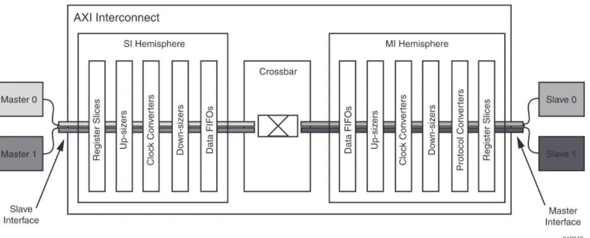
AXI Interconnect Core Diagrams
Figure 2-6 illustrates a top-level AXI Interconnect.
AXI Interconnect Core Use Models
The AXI Interconnect IP core connects one or more AXI memory-mapped master devices to one or more memory-mapped slave devices. The following subsections describe the possible use cases:
• Pass Through • Conversion Only • N-to-1 Interconnect • 1-to-N Interconnect
• N-to-M Interconnect (Sparse Crossbar) • N-to-M Interconnect (Shared Access Mode)
Figure 2-6: Top-Level AXI Interconnnect
AXI Interconnect
Slave
Interface InterfMasterace
SI Hemisphere MI Hemisphere
Crossbar Master 0 Slave 0 Slave 1 Master 1 Regi s ter S lice s Regi s ter S lice s Up-s iz er s Up-s iz er s Cloc k Con v e rter s Do wn-s iz er s D a t a FIFO s Cloc k Con v e rter s Do wn-s iz er s Protocol Con v e rter s D a t a FIFO s X12047
Pass Through
When there is one master device and one slave device only connected to the AXI Interconnect, and the AXI Interconnect core is not performing any optional conversion functions or pipelining, the AXI Interconnect core degenerates into direct wire connections with no latency and consuming no logic resources.
Figure 2-7 shows the Pass Through diagram.
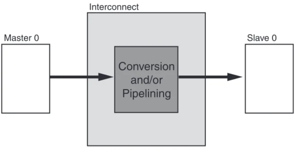
Conversion Only
The AXI Interconnect core can perform various conversion and pipelining functions when connecting one master device to one slave device. These are:
• Data width conversion • Clock rate conversion • AXI4-Lite slave adaptation • AXI-3 slave adaptation
• Pipelining, such as a register slice or data channel FIFO
In these cases, the AXI Interconnect core contains no arbitration, decoding, or routing logic. There could be latency incurred, depending on the conversion being performed.
Figure 2-8 shows the one-to-one or conversion use case.
Figure 2-7: Pass-through AXI Interconnect Use Case
Figure 2-8: 1-to-1 Conversion AXI Interconnect Use Case
Master 0 Slave 0 Interconnect X12049 Master 0 Slave 0 Interconnect
Conver
s
ion
a
nd/or
Pipelining
N-to-1 Interconnect
A common degenerate configuration of AXI Interconnect core is when multiple master devices arbitrate for access to a single slave device, typically a memory controller. In these cases, address decoding logic might be unnecessary and omitted from the AXI Interconnect core (unless address range validation is needed).
Conversion functions, such as data width and clock rate conversion, can also be performed in this configuration. Figure 2-9 shows the N to 1 AXI interconnection use case.
.
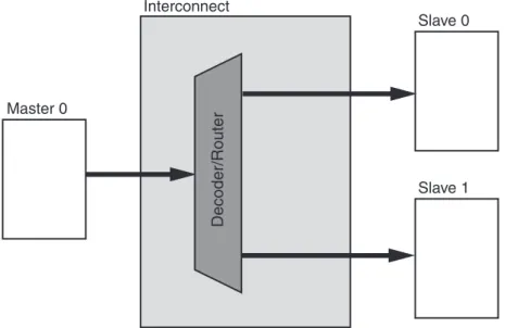
1-to-N Interconnect
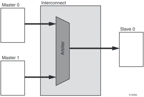
Another degenerative configuration of the AXI Interconnect core is when a single master device, typically a processor, accesses multiple memory-mapped slave peripherals. In these cases, arbitration (in the address and Write data paths) is not performed. Figure 2-10, page 25, shows the 1 to N Interconnect use case.
Figure 2-9: N-to-1 AXI Interconnect
X12050 Master 0 Master 1 Slave 0 Interconnect Ar b iter
N-to-M Interconnect (Sparse Crossbar)
AXI Interconnect features a Shared-Address Multiple-Data (SAMD) topology, consisting of sparse data crossbar connectivity, with single-threaded Write and Read address
arbitration, as shown in Figure 2-11.
Figure 2-12, page 26 shows the sparse crossbar Write and Read data pathways.
Figure 2-10: 1-to-N AXI Interconnect Use Case
X12051 Master 0 Slave 0 Slave 1 Interconnect Decoder/Ro u ter
Figure 2-11: Shared Write and Read Address Arbitration
X12052 Master 0 Master 1 Master 2 Slave 0 Slave 1 Slave 2 Interconnect AW AR AW AR AW AR AW AR AW AR AW AR Write Transaction Arbiter Read Transaction Arbiter Router Router
Parallel Write and Read data pathways connect each SI slot (attached to AXI masters on the left) to all the MI slots (attached to AXI slaves on the right) that it can access, according to the configured sparse connectivity map. When more than one source has data to send to different destinations, data transfers can occur independently and concurrently, provided AXI ordering rules are met.
The Write address channels among all SI slots (if > 1) feed into a central address arbiter, which grants access to one SI slot at a time, as is also the case for the Read address channels. The winner of each arbitration cycle transfers its address information to the targeted MI slot and pushes an entry into the appropriate command queue(s) that enable various data pathways to route data to the proper destination while enforcing AXI ordering rules.
Width Conversion
The AXI Interconnect core has a parametrically-defined, internal, native data-width that supports 32, 64, 128, and 256 bits. The AXI data channels that span the crossbar are sized to the “native” width of the AXI Interconnect, as specified by the
C_INTERCONNECT_DATA_WIDTH parameter.
When any SI slots or MI slots are sized differently, the AXI Interconnect core inserts width conversion units to adapt the slot width to the AXI Interconnect core native width before transiting the crossbar to the other hemisphere.
The width conversion functions differ depending on whether the data path width gets wider (“up-sizing”) or more narrow (“down-sizing”) when moving in the direction from the SI toward the MI. The width conversion functions are the same in either the SI hemisphere (translating from the SI to the AXI Interconnect core native width) or the MI hemisphere (translating from the AXI Interconnect core native width to the MI).
Figure 2-12: Sparse Crossbar Write and Read Data Pathways
X12053 Interconnect Master 0 Master 1 Master 2 Slave 0 Slave 1 Slave 2 W R W R W R W R W R W R
Write Data Crossbar
MI and SI slots have an associated individual parametric data-width value. The AXI Interconnect core adapts each MI and SI slot automatically to the internal native data-width as follows:
• When the data width of an SI slot is wider than the internal native data width of the AXI Interconnect, a down-sizing conversion is performed along the pathways of the SI slot.
• When the internal native data width of the AXI Interconnect core is wider than that of an MI slot, a down-sizing conversion is performed along the pathways of the MI slot. • When the data width of an SI slot is narrower than the internal native data width of
the AXI Interconnect, an up-sizing conversion is performed along the pathways of the SI slot.
• When the internal native data width of the AXI Interconnect core is narrower than that of an MI slot, an up-sizing conversion is performed along the pathways of the MI slot.
Typically, the data-width of the AXI Interconnect core is matched to the smaller of the widest SI slot or the widest MI slot in the system design.
The following subsections describe the down-sizing and up-sizing behavior.
Downsizing
Downsizers used in pathways connecting wide master devices are equipped to split burst transactions that might exceed the maximum AXI burst length (even if such bursts are never actually needed). When the data width on the SI side is wider than that on the MI side and the transfer size of the transaction is also wider than the data width on the MI side, then down-sizing is performed and, in the transaction issued to the MI side, the number of data beats is multiplied accordingly.
• For writes, data serialization occurs • For reads, data merging occurs
When the transfer size of the transaction is equal to or less than the MI side data width, the transaction (address channel values) remains unchanged, and data transfers pass through unchanged except for byte-lane steering. This applies to both writes and reads.
Upsizing
For upsizers in the SI hemisphere, data packing is performed (for INCR and WRAP bursts), provided the AW/ARCACHE[1] bit (“Modifiable”) is asserted.
In the resulting transaction issued to the MI side, the number of data beats is reduced accordingly.
• For writes, data merging occurs. • For reads, data serialization occurs.
N-to-M Interconnect (Shared Access Mode)
When in Shared Access mode, the N-to-M use case of the AXI Interconnect core provides for only one outstanding transaction at a time, as shown in Figure 2-13, page 28. For each connected master, Read transaction requests always take priority over Writes. The arbiter then selects from among the requesting masters. A Write or Read data transfer is enabled to the targeted slave device. After the data transfer (including the Write response) completes, the next request is arbitrated.
Shared Access mode minimizes the resources used to implement the crossbar module of the Interconnect. Figure 2-13 illustrates the Shared Access mode.
Clock Conversion
Clock conversion comprises the following:
• A clock-rate reduction module performs integer (N:1) division of the clock rate from its input (SI) side to its output (MI) side.
• A clock-rate acceleration module performs integer (1:N) multiplication of clock rate from its input (SI) to output (MI) side.
• An asynchronous clock conversion module performs either reduction or acceleration of clock-rates by passing the channel signals through an asynchronous FIFO.
For both the reduction and the acceleration modules, the sample cycle for the faster clock domain is determined automatically. Each module is applicable to all five AXI channels. The MI and SI each have a vector of clock inputs in which each bit synchronizes all the signals of the corresponding interface slot. The AXI Interconnect core has its own native clock input. The AXI Interconnect core adapts the clock rate of each MI and SI slot automatically to the native clock rate of the AXI Interconnect.
Typically, the native clock input of the AXI Interconnect core is tied to the same clock source as used by the highest frequency SI or MI slot in the system design, such as the MI slot connecting to the main memory controller.
Pipelining
Under some circumstances, AXI Interconnect core throughput is improved by buffering data bursts. This is commonly the case when the data rate at a SI or MI slot differs from the native data rate of the AXI Interconnect core due to data width or clock rate conversion. To accommodate the various rate change combinations, data burst buffers can be inserted optionally at the various locations.
Additionally, an optional, two-deep register slice (skid buffer) can be inserted on each of the five AXI channels at each SI or MI slot to help improve system timing closure.
Figure 2-13: Shared Access Mode
-ASTER -ASTER 3LAVE 3LAVE !7 !2 7 2 !7 !2 7 2 !7 !2 7 2 !7 !2 7 2 )NTERCONNECT !RBITER !DDRESS 7RITE$ATA 2EAD$ATA
Peripheral Register Slices
At the outer-most periphery of both the SI and MI, each channel of each interface slot can be optionally buffered by a register slice. These are provided mainly to improve system timing at the expense of one latency cycle.
Peripheral register slices are always synchronized to the SI or MI slot clock.
Data Path FIFOs
To accommodate the data flow rate change combinations between the SI and MI sides of the AXI Interconnect core, data path buffers can be inserted optionally at the following four locations:
• The SI-side Write data FIFO is located before the Write data router of each SI slot. • The MI-side Write data FIFO is located after the Write data multiplexer of each MI
slot.
• The MI-side Read data FIFO is located before (on the MI side of) the Read data router of each MI slot.
• The SI-side Read data FIFO is located after (on the SI side of) the Read data
multiplexers of each SI slot, including the MUX between multiple ID-thread pathways for multi-threaded SI slots.
Data FIFOs are synchronized to the AXI Interconnect core native clock. The width of each data FIFO matches the AXI Interconnect core native data width.
For more detail and the required signals and parameters of the AXI Interconnect core IP, refer to the AXI Interconnect IP (DS768), available at the Xilinx website:
http://www.xilinx.com/support/documentation/axi_ip_documentation.htm.
Connecting AXI Interconnect Core Slaves and Masters
You can connect the slave interface of one AXI Interconnect core module to the master interface of another AXI Interconnect core with no intervening logic using an AXI-to-AXI Connector (axi2axi_connector) IP. The axi2axi_connector IP provides the port connection points necessary to represent the connectivity in the system, plus a set of parameters used to configure the respective interfaces of the AXI Interconnect core modules being
connected.),
AXI-To-AXI Connector Features
The features of the axi2axi_connector are:• Connects the master interface of one AXI Interconnect core module to slave interface of another AXI Interconnect core module.
• Directly connects all master interface signals to all slave interface signals. • Contains no logic or storage, and functions as a bus bridge in EDK.
Description
The AXI slave interface of the axi2axi_connector (“connector”) module always connects to one attachment point (slot) of the master interface of one AXI Interconnect core module (the “upstream interconnect”). The AXI master interface of the connector always connects to one slave interface slot of a different AXI Interconnect core module (the “downstream interconnect”)as shown in Figure 2-14, page 30.
Using the AXI To AXI Connector
When using the AXI To AXI Connector (axi2axi_connector) you can cascade two AXI Interconnect cores. The EDK tools set the data width and clock frequency parameters on the axi2axi_connector IP so that the characteristics of the master and slave interfaces match.
Also, the EDK tools auto-connect the clock port of the axi2axi_connector so that the interfaces of the connected interconnect modules are synchronized by the same clock source.
For more detail and the required signals and parameter of the AXI To AXI Connector, refer to the AXI To AXI Connector IP Data Sheet (DS803), available at the Xilinx website:
http://www.xilinx.com/support/documentation/axi_ip_documentation.htm.
External Masters and Slaves
When there is an AXI master or slave IP module that is not available as an EDK pcore (such as a pure HDL module) that needs to be connected to an AXI Interconnect core inside the EDK sub-module, these utility cores can be used for that the purpose. The AXI master or slave module would remain in the top-level of the design, and the AXI signals would be connected to the EDK sub system using this utility pcore.
Features
• Connects an AXI master or slave interface to the AXI Interconnect core IP. • A master or slave AXI bus interface on one side and AXI ports on the other side. • Other ports are modeled as an I/O interface, which can be made external, thereby
providing the necessary signals that can be connected to a top-level master or slave.
Figure 2-14: Master and Slave Interface Modules Connecting Two AXI Interconnect cores
mb_0 AXI_Interconnect_0 AXI_Interconnect_1 AXI_Interconnect_2 slave_2 axi2axi_connector slave_1 slave_3 M_AXI_IP M_AXI_DP M_AXI_IC M_AXI_DC X12036
Figure 2-15, page 31 is a block diagram of the AXI external master connector.
Figure 2-16 shows a block diagram of the external slave connector.
The Platform Studio IP Catalog contains the external master and external slave connectors. For more information, refer to the Xilinx website:
http://www.xilinx.com/ipcenter/axi4.htm.
Figure 2-15: EDK Sub-system using an External Master Connector
Individual AXI Ports made external to sub-system
interface
Microblaze
EDK sub-system
Axi_ext_master_conn ICAXI DCAXI S_AXI M_AXI Memory controller Axi_interconnect X12040
Figure 2-16: EDK Subsystem using an External Slave Connector
Microblaze
Axi_interconnect
ICAXI S_AXI Memory controller
DCAXI EDK sub-system
Individual AXI Ports made external to sub-system
interface Axi_gpio Axi_ext_slave_conn S_AXI S_AXI X12075
Centralized DMA
Xilinx provides a Centralized DMA core for AXI. This core replaces legacy PLBv4.6 Centralized DMA with an AXI4 version that contains enhanced functionality and higher performance. Figure 2-17 shows a typical embedded system architecture incorporating the AXI (AXI4 and AXI4-Lite) Centralized DMA.
The AXI4 Centralized DMA performs data transfers from one memory mapped space to another memory mapped space using high speed, AXI4, bursting protocol under the control of the system microprocessor.
Figure 2-17: Typical Use Case for AXI Centralized DMA
AXI CDMA CPU (AXI MicroBlaze) AXI4 MMap Interconnect (AXI4-Lite) AXI BRAM AXI DDRx Registers Scatter Gather Engine AXI4 AXI4 AXI4 Read AXI4 Write AXI4-Lite AXI4 AXI Intc AXI4-Lite AXI4-Lite AXI4 MMap Interconnect (AXI4) DP DC IC AXI4 AXI4 Interrupt Interrupts In Interrupt Out (To AXI Intc)
AXI4-Stream
AXI4-Stream
DataMover
AXI Centralized DMA Summary
The AXI Centralized DMA provides the same simple transfer mode operation as the legacy PLBv4.6 Centralized DMA. A simple mode transfer is defined as that which the CPU programs the Centralized DMA register set for a single transfer and then initiates the transfer. The Centralized DMA:
• Performs the transfer
• Generates an interrupt when the transfer is complete
• Waits for the microprocessor to program and start the next transfer
Also, the AXI Centralized DMA includes an optional data realignment function for 32- and 64-bit bus widths. This feature allows addressing independence between the transfer source and destination addresses.
AXI Centralized DMA Scatter Gather Feature
In addition to supporting the legacy PLBv4.6 Centralized DMA operations, the AXI Centralized DMA has an optional Scatter Gather (SG) feature.
SG enables the system CPU to off-load transfer control to high-speed hardware automation that is part of the Scatter Gather engine of the Centralized DMA. The SG function fetches and executes pre-formatted transfer commands (buffer descriptors) from system memory as fast as the system allows with minimal required CPU interaction. The architecture of the Centralized DMA separates the SG AXI4 bus interface from the AXI4 data transfer interface so that buffer descriptor fetching and updating can occur in parallel with ongoing data transfers, which provides a significant performance enhancement. DMA transfer progress is coordinated with the system CPU using a programmable and flexible interrupt generation approach built into the Centralized DMA. Also, the AXI Centralized DMA allows the system programmer to switch between using Simple Mode transfers and SG-assisted transfers using the programmable register set.
The AXI Centralized DMA is built around the new high performance AXI DataMover helper core which is the fundamental bridging element between AXI4-Stream and AXI4 memory mapped buses. In the case of AXI Centralized DMA, the output stream of the DataMover is internally looped back to the input stream. The SG feature is based on the Xilinx SG helper core used for all Scatter Gather enhanced AXI DMA products.
Centralized DMA Configurable Features
The AXI4 Centralized DMA lets you trade-off the feature set implemented with the FPGA resource utilization budget. The following features ar e parameterizable at FPGA
implementation time:
• Use DataMover Lite for the main data transport (Data Realignment Engine (DRE)and SG mode are not supported with this data transport mechanism)
• Include or omit the Scatter Gather function
• Include or omit the DRE function (only available for 32- and 64-bit data transfer bus widths)
• Specify the main data transfer bus width (32, 64, 128, or 256 bits)
• Specify the maximum allowed AXI4 burst length the DataMover will use during data transfers
Centralized DMA AXI4 Interfaces
The following table summarizes the four external AXI4 Centralized DMA interfaces in addition to the internally-bridged DataMover stream interface within the AXI Centralized DMA function.
Ethernet DMA
The AXI4 protocol adoption in Xilinx embedded processing systems contains an Ethernet solution with Direct Memory Access (DMA). This approach blends the performance advantages of AXI4 with the effective operation of previous Xilinx Ethernet IP solutions. Figure 2-18, page 35 provides high-level block diagram of the AXI DMA.
Table 2-1: AXI Centralized DMA AXI4 Interfaces
Interface AXI Type Data Width Description
Control AXI4-Lite slave 32
Used to access the AXI Centralized DMA internal registers. This is generally used by the system processor to control and monitor the AXI Centralized DMA operations.
Scatter Gather AXI4 master 32
An AXI4 memory mapped master that is used by the AXI Centralized DMA to read DMA transfer descriptors from System Memory and then to write updated descriptor information back to System Memory when the associated transfer operation has completed.
Data MMap Read AXI4 Read master
32, 64, 128, 256
Reads the transfer payload data from the memory mapped source address. The data width is parameterizable to be 32, 64, 128, and 256 bits wide.
Data MMap Write AXI4 Write master
32, 64, 128, 256
Writes the transfer payload data to the memory mapped destination address. The data width is parameterizable to be 32, 64, 128, and 256 bits wide, and is the same width as the Data Read interface.
Figure 2-19 shows a typical system architecture for the AXI Ethernet.
Figure 2-18: AXI DMA High Level Block Diagram
AXI DMA S2MM DMA Controller MM2S DMA Controller AXI DataMover AXI L ite S l a ve Inte rf a ce MM2S_IntrOut S2MM_IntrOut Reset Module
Register Module
MM2S_DMACR MM2S_DMASR MM2S_CURDESC Reserved MM2S_TAILDESC Reserved S2MM_DMACR S2MM_DMASR S2MM_CURDESC Reserved S2MM_TAILDESC Reserved AXI C o n tr o l In te rf a ce AXI S t a t us Inte rf a ce SG Engine (Interrupt Coalescing) SG Interface AXI Memory Map Read (MM2S)
AXI Memory Map Write (S2MM)
AXI Control Stream (MM2S) AXI StatusStream (S2MM) AXI Stream (MM2S) AXI Stream (S2MM) AXI Lite
AXI Memory Map SG Read / Write
SG Interface
X12038
Figure Top x-ref 3
Figure 2-19: Typical Use Case for AXI DMA and AXI4 Ethernet
CPU (AXI MicroBlaze) AXI4 MMap Interconnect AXI Ethernet AXI BRAM AXI DDRx Registers AXI DMA Scatter Gather Engine DataMover Ethernet Control and Status Registers AXI4-Lite AXI4-Stream AXI4-Stream AXI4-Stream AXI4-Stream Tx Payload Rx Payload Tx Control Rx Status AXI Intc AXI4 MMap Interconnect DP DC IC AXI4 Interrupt Interrupts In Interrupt Out (To AXI Intc)
Interrupt Out (To AXI Intc)
AXI4-Stream AXI4-Stream AVB Ethernet Tx Ethernet Rx MIIM AXI4-Lite AXI4-Lite AXI4-Lite AXI4 AXI4 AXI4 AXI4 AXI4 Read AXI4 Write X12039
As shown in Figure 2-19, page 35, the AXI Ethernet is now paired with a new AXI DMA IP. The AXI DMA replaces the legacy PLBv4.6 SDMA function that was part of the PLBv4.6 Multi-Port Memory Controller (MPMC).
The AXI DMA is used to bridge between the native AXI4-Stream protocol on the AXI Ethernet to AXI4 memory mapped protocol needed by the embedded processing system.
AXI4 DMA Summary
The AXI DMA engine provides high performance direct memory access between system memory and AXI4-Stream type target peripherals. The AXI DMA provides Scatter Gather (SG) capabilities, allowing the CPU to offload transfer control and execution to hardware automation.
The AXI DMA as well as the SG engines are built around the AXI DataMover helper core (shared sub-block) that is the fundamental bridging element between AXI4-Stream and AXI4 memory mapped buses.
AXI DMA provides independent operation between the Transmit channel Memory Map to Slave (MM2S) and the Receive channel Slave to Memory Map (S2MM), and provides optional independent AXI4-Stream interfaces for offloading packet metadata.
An AXI control stream for MM2S provides user application data from the SG descriptors to be transmitted from AXI DMA.
Similarly, an AXI status stream for S2MM provides user application data from a source IP like AXI4 Ethernet to be received and stored in a SG descriptors associated with the Receive packet.
In an AXI Ethernet application, the AXI4 control stream and AXI4 status stream provide the necessary functionality for performing checksum offloading.
Optional SG descriptor queuing is also provided, allowing fetching and queuing of up to four descriptors internally in AXI DMA. This allows for very high bandwidth data transfer on the primary data buses.
DMA AXI4 Interfaces
The Xilinx implementation for DMA uses the AXI4 capabilities extensively.The following table summarizes the eight AXI4 interfaces used in the AXI DMA function.
Table 2-2: AXI DMA Interfaces
Interface AXI Type Data
Width Description
Control AXI4-Lite slave 32 Used to access the AXI DMA internal registers. This is generally used by the System Processor to control and monitor the AXI DMA operations.
Scatter Gather AXI4 master 32 An AXI4 memory mapped master used by the AXI4 DMA to Read DMA transfer descriptors from system memory and Write updated descriptor information back to system memory when the associated transfer
operation is complete. Data MM Read AXI4 Read
master
32, 64, 128, 256
Transfers payload data for operations moving data from the memory mapped side of the DMA to the Main Stream output side.
Data MM Write AXI4 Write master
32, 64, 128, 256
Transfers payload data for operations moving data from the Data Stream In interface of the DMA to the memory mapped side of the DMA.
Data Stream Out AXI4-Stream master
32, 64, 128, 256
Transfers data read by the Data MM Read interface to the target receiver IP using the AXI4-Stream protocol. Data Stream In AXI4-Stream
slave
32, 64, 128, 256
Received data from the source IP using the AXI4-Stream protocol. Transferred the received data to the Memory Map system using the Data MM Write Interface. Control Stream Out AXI4-Stream
master
32 The Control stream Out is used to transfer control information imbedded in the Tx transfer descriptors to the target IP.
Status Stream In AXI4-Stream slave
32 The Status Stream In receives Rx transfer information from the source IP and updates the data in the associated transfer descriptor and written back to the System Memory using the Scatter Gather interface during a descriptor update.
Video DMA
The AXI4 protocol Video DMA (VDMA) provides a high bandwidth solution for Video applications. It is a similar implementation to the Ethernet DMA solution.
Figure 2-20 shows a top-level AXI4 VDMA block diagram.
Figure 2-21, page 39 illustrates a typical system architecture for the AXI VDMA.
Figure 2-20: AXI VDMA High-Level Block Diagram
AXI VDMA S2MM DMA Controller MM2S DMA Controller AXI DataMover AXI Lite S l a ve Interf a ce MM2S_IntrOut S2MM_IntrOut Reset Module Register Module
MM2S_DMACR MM2S_DMASR MM2S_CURDESC S2MM_DMACR S2MM_DMASR S2MM_CURDESC Reserved SG Engine (Interrupt Coalescing ) AXI Memory Map Read (MM2S)
AXI Memory Map Write (S2MM)
AXI MM2S Stream AXI S2MM Stream AXI Lite AXI Memory Map SG Read MM2S Gen-Lock MM2S FSync S2MM Gen-Lock S2MM FSync MM2S_TAILDESC Reserved S2MM_TAILDESC Reserved MM2S Frame Size MM2SStride MM2SStrt Addr 0 MM2SStrt Addr N : MM2S Frame Size MM2SStride MM2SStrt Addr 0 MM2SStrt Addr N : MM2S Frame Size MM2SStride MM2SStrt Addr 0 MM2SStrt Addr N : MM2S Frame Size MM2SStride MM2SStrt Addr 0 MM2SStrt Addr N : axi_resetn m_axis_mm2s_aresetn s_axis_s2mm_aresetn Line Buffer Line Buffer MM2S Line Bufffer Status S2MM Line Bufffer Status Down Sizer Up Sizer Reserved x12054
AXI VDMA Summary
The AXI VDMA engine provides high performance direct memory access between system memory and AXI4-Stream type target peripherals. The AXI VDMA provides Scatter Gather (SG) capabilities also, which allows the CPU to offload transfer control and execution to hardware automation. The AXI VDMA and the SG engines are built around the AXI DataMover helper core which is the fundamental bridging element between AXI4-Stream and AXI4 memory mapped buses.
AXI VDMA provides circular frame buffer access for up to 16 frame buffers and provides the tools to transfer portions of video frames or full video frames.
The VDMA provides the ability to “park” on a frame also, allowing the same video frame data to be transferred repeatedly.
VDMA provides independent frame synchronization and an independent AXI clock, allowing each channel to operate on a different frame rate and different pixel rate. To maintain synchronization between two independently functioning AXI VDMA channels, there is an optional Gen-Lock synchronization feature.
Gen-Lock provides a method of synchronizing AXI VDMA slaves automatically to one or more AXI VDMA masters such that the slave does not operate in the same video frame buffer space as the master. In this mode, the slave channel skips or repeats a frame automatically. Either channel can be configured to be a Gen-Lock slave or a Gen-Lock master.
For video data transfer, the AXI4-Stream ports can be configured from 8 bits up to 256 bits wide. For configurations where the AXI4-Stream port is narrower than the associated AXI4 memory map port, the AXI VDMA upsizes or downsizes the data providing full bus width burst on the memory map side.
Figure 2-21: Typical Use Case for AXI VDMA and Video IP
&IGURE4OPXREF !8))NTERCONNECT !8)$$2X #05 !8) -ICRO"LAZE !8)"2!-6IDEO 4IMING #ONTROLLER 6IDEO)0 !8) !8) !8))NTC )NTERRUPT )NTERRUPTS)N !8)--AP )NTERCONNECT !8),ITE !8),ITE $0 $# )# !8) !8) 2EGISTERS 3CATTER 'ATHER %NGINE $ATA-OVER --3 #ONTROLLER --3 'EN,OCK 3--#ONTROLLER 3--'EN,OCK 6IDEO)0 'EN,OC K )NTERRUPT/UT 4O!8))NTC !8)6$-! --3&3YNC 6IDEO 4IMING #ONTROLLER 3--&SYNC !8),ITE !8)7RITE !8)3TREAM !8)3TREAM !8)2EAD !8)2EAD 6IDEO/UT 6IDEO)N 8
VDMA AXI4 Interfaces
Table 2-3 lists and describes six AXI4 interfaces of the AXI DMA function.
Memory Control IP and the Memory Interface Generator
There are two DDRx (SDRAM) AXI memory controllers available in the IP catalog. Because the Virtex-6 and Spartan-6 devices have natively different memory control mechanisms (Virtex-6 uses a fabric-based controller and Spartan-6 has an on-chip Memory Control Block (MCB)), the description of memory control is necessarily device-specific. The following subsections describe AXI memory control by Virtex-6 and Spartan-6 devices.
The Virtex-6 and Spartan-6 memory controllers are available in two different software packages:
• In EDK, as the axi_v6_ddrx or the axi_s6_ddrx memory controller core.
• In the CORE™ Generator interface, through the Memory Interface Generator (MIG) tool.
The underlying HDL code between the two packages is the same with different wrappers. The flexibility of the AXI4 interface allows easy adaptation to both controller types.
Table 2-3: AXI VDMA Interfaces
Interface AXI Type Data Width Description
Control AXI4-Lite slave 32 Accesses the AXI VDMA internal registers. This is generally used by the System Processor to control and monitor the AXI VDMA operations.
Scatter Gather AXI4 master 32 An AXI4 memory mapped master that is used by the AXI VDMA to read DMA transfer descriptors from System Memory. Fetched Scatter Gather descriptors set up internal video transfer parameters for video transfers.
Data MM Read AXI4 Read master 32, 64, 128, 256
Transfers payload data for operations moving data from the memory mapped side of the DMA to the Main Stream output side.
Data MM Write AXI4 Write master
32, 64, 128, 256
Transfers payload data for operations moving data from the Data Stream In interface of the DMA to the memory mapped side of the DMA.
Data Stream Out AXI4-Stream master
8,16, 32, 64, 128, 256
Transfers data read by the Data MM Read interface to the target receiver IP using the AXI4-Stream protocol.
Data Stream In AXI4-Stream slave
8, 16, 32, 64, 128, 256
Receives data from the source IP using the AXI4-Stream protocol. The data received is then transferred to the Memory Map system via the Data MM Write Interface.