ABSTRACT
RAHEJA, UTKARSH. Design of a GaN FET Based LLC Resonant Converter for Point Of Load Conversion. (Under the direction of Dr. Subhashish Bhattacharya).
This thesis presents the converter and control design for an LLC resonant converter based on GaN
devices for Point-Of-Load (POL) conversion applications. This topology has been extensively
developed in literature for POL applications for Data Centers. However, due to advantages like
ability to achieve primary-side ZVS (Zero-Voltage Switching) throughout the load range and input
voltage range, high efficiency even at light loads (10%), operate at high switching frequencies
allowing improved power densities, it has become a popular candidate for automotive POL
applications. The converter developed in this thesis is the prototype for a POL converter in a
Distributed Power System of a Heavy-Duty vehicle like Tractor.
With the ability to operate under ZVS, the switching losses can be reduced to negligible values.
However, conduction losses are not mitigated, which can reduce achievable efficiency. This
provides the motivation to use GaN devices, due to the extremely low on-state resistance,
especially for the low-voltage, high current devices on the secondary-side. There is an additional
advantage of absence of reverse recovery losses, which can reduce efficiency above resonant
frequency operation. This thesis work presents a design methodology for the selection of the
resonant tank parameters, an approach for small-signal modelling and voltage-mode control design
based on variable frequency control. Also, in order to take advantage of the low on-state resistance
of the GaN devices, a digital implementation approach is also detailed. Finally, specifics of the
hardware implementation, including the layout recommendations for Gate-drive design and
Power-loop design are illustrated, as an aid for future work using similar GaN devices. The control
and modelling have been verified by comparison between response from hardware results,
© Copyright 2018 Utkarsh Raheja
Design of a GaN FET Based LLC Resonant Converter for Point Of Load Conversion Applications
By Utkarsh Raheja
A thesis submitted to the Graduate Faculty of North Carolina State University
in partial fulfillment of the requirements for the degree of
Master of Science
Electrical Engineering
Raleigh, North Carolina
2018
APPROVED BY:
_______________________________ Dr. Subhashish Bhattacharya
Committee Chair
_______________________________ _______________________________
DEDICATION
BIOGRAPHY
Utkarsh Raheja was born on March 14, 1992 in New Delhi, India. He did his schooling from DPS
R.K. Puram School, New Delhi. He graduated from Delhi Technological University, New Delhi
with a Bachelor in Electrical and Electronics Engineering. He joined North Carolina State
University in 2016 for M.S. in Electrical Engineering with specialization in Power Electronics.
Since Feb 2016, he has been associated with Future Renewable Electrical Energy Delivery and
Management (FREEDM) Systems Center during his study at North Carolina State University. His
ACKNOWLEDGMENTS
I express my sincere gratitude and thank my advisor, Dr. Subhashish Bhattacharya for the guidance
he has provided me during my graduate program at North Carolina State University. Working with
Dr Bhattacharya has been an insightful experience and he gave me good opportunities to work on
different projects including Characterization of a GaN based Four-Quadrant Switch, GaN based
H-Bridge design for Secondary side of a DAB converter and GaN based LLC resonant converter
for POL applications. I thank Dr. Douglas Hopkins and Dr. Jayant Baliga for being a member of
the committee and taking the time to review my thesis and providing valuable inputs.
I thank FREEDM Systems Center for sharing the resources for this project. I want to thank Dr.
Ghanshyamsinh Gohil for his guidance and help. I appreciate the valuable suggestions from my
seniors and friends, Abhay Negi, Suyash Shah, Vishnu Mahadeva Iyer, Srinivas Gulur, Ashish
Kumar, Anup Anurag, Sayan Acharya, Yos Prabowo, Ritwik Chattopadhyay, Rishabh Jain at
FREEDM Systems Center. I extend my gratitude towards the staff members of the center,
especially Karen Autry for all her support. I thank Hulgize Kassa for his supervision ensuring my
safety in the laboratory. I thank Rajat, Shashank, Ayush, Sukhmeet, Samyak and others for making
this journey a memorable one. I would like to thank my family members for their constant support
TABLE OF CONTENTS
LIST OF TABLES………...vii
LIST OF FIGURES………viii
1. Introduction ... 1
1.1Background and Motivation ... 1
1.2 Thesis Outline ... 4
2. Operating Principle And Design of LLC Resonant Converter ... 5
2.1Principle of Operation ... 5
2.1.1 Operation below Resonant Frequency (Fs<F0) ... 5
2.1.2 Operation at Resonant Frequency (Fs = F0) ... 7
2.1.3 Operation above Resonant Frequency (Fs > F0) ... 8
2.2 Design Equations and Methodology ... 10
2.2.1 Design Methodology ... 11
3. Small-Signal Modelling and Controller Design... 16
3.1 Extended Describing Function Method ... 16
3.2 Controller design ... 25
3.3 Discretization and Digital Controller Implementation ... 29
4. Synchronous Rectification ... 31
4.1 Digital Implementation Algorithm ... 32
4.2 Layout Recommendation ... 35
4.3 Implementation on TI-TMS320f28335 ... 36
5.1 Gate Drive Design ... 38
5.2 Power Loop Design ... 40
5.3 Parameter Measurement for Transformer and Inductor ... 41
5.4 Hardware Results ... 45
5.4.1 Open Loop Response ... 45
5.4.2 Closed Loop Response ... 47
5.4.2.1 Step Change in VREF ... 47
5.4.2.2 Step Change in Load ... 49
5.4.2.3 Measured Efficiency ... 49
6. Applications and Characterization of Four-Quadrant GaN Switch………...51
6.1 Four Quadrant Switch ... 54
6.2 Static Characteristics ... 58
6.3 Dynamic Characteristics ... 61
6.3.1 Double Pulse Test Circuit ... 61
6.3.2 Switching Energies ... 64
6.4 Conclusion ... 69
LIST OF TABLES
Table 2.1
Table 2.2
Table 3.1
Table 5.1
Converter prototype specifications………...
Frequency range of operation, Peak magnetizing current and resonant tank
parameter values for different designs under consideration………...
Loop gain parameters for the designed controller for the four corner cases………...
Measured parameters for the transformer and inductor used in the prototype……… 12
14
27
LIST OF FIGURES Figure 1.1 Figure 1.2 Figure 2.1 Figure 2.2 Figure 2.3 Figure 2.4 Figure 2.5 Figure 2.6 Figure 2.7 Figure 2.8 Figure 3.1 Figure 3.2 Figure 3.3 Figure 3.4
Power Supply Architecture for a Heavy-Duty Vehicle ...
(a) Phase-shifted Full-Bridge converter (b) LLC resonant converter. Two possible
candidates for POL applications in Heavy Duty Vehicle applications ...
Schematic for LLC resonant converter...
Output voltage from H-bridge, resonant tank current and magnetizing current
(fs<f0) ...
Output voltage of H-bridge, resonant tank current and magnetizing current
(fS=f0)……….
Output voltage of H-bridge, resonant tank current and magnetizing current (fS>f0)
Drop in resonant current at turn-off instant of Q2 and Q3 switches ...
Impedance curve for series resonant tank ...
Equivalent resonant circuit for computing DC gain...
Plot of peak gain vs Qmax for different values of m……….
Equivalent circuit of LLC resonant converter ...
Large-signal model of LLC resonant converter ...
Bode plot for converter control-to-output transfer function (@Vin = 270V, Pload =
500W)………
(a) Loop-gain bode plot for converter design with output capacitor of 470µF and
cross-over frequency beyond double pole frequency. (PM: 63.3 deg, GM: 10.6dB,
cross-over: 20.3 kHz) (b) Simulation results for step change in load from 30% to
Figure 3.5 Figure 3.6 Figure 3.7 Figure 3.8 Figure 4.1 Figure 4.2 Figure 4.3 Figure 4.4 Figure 5.1 Figure 5.2 Figure 5.3 Figure 5.4 Figure 5.5 Figure 5.6 Figure 5.7 Figure 5.8
Loop-gain bode plot for converter design with output capacitor of 72µF and
cross-over frequency below double pole frequency. (PM: 88.6 deg, GM: 32.9dB,
cross-over: 1.67 kHz) ...
Bode plot of a complex lead compensator (damping constant: 0.707) ...
Discretized model of the converter system using Tustin approximation (sampling
frequency: 175 kHz) along with continuous domain model ...
Loop-gain bode plot for controller designed with discretized system model (PM:
83.4 deg, GM: 13.3dB, cross-over: 1.51 kHz) ...
Diode conduction detection circuit (enclosed in dashed rectangle) ...
Synchronous rectification algorithm flow chart...
Layout recommendation for diode conduction detection circuit. Path 1 used for
forward path with kelvin connected return path overlapped with forward path ...
DSP implementation of synchronous rectification algorithm...
Picture of the Hardware test setup for LLC resonant converter ...
Gate Loop Design ...
Power Loop design for Primary-side H-Bridge ...
Impedance plot for resonant inductor ...
Impedance plot for transformer (secondary open-circuited) ...
Impedance plot for transformer (secondary short-circuited) ...
Resonant tank and transformer model extracted from measurements ...
Converter operation at Vin = 270V and Rload = 1.4Ω. Resonant tank current
Figure 5.9 Figure 5.10 Figure 5.11 Figure 5.12 Figure 5.13 Figure 5.14 Figure 5.15
(blue and pink). Fixed Synch rectification pulses are given equal to resonant half
period minus safety margin...
Converter operation at Vin = 270V and Rload = 1.4Ω. Resonant Tank current
(Yellow), Voltage applied to resonant tank (Green), Vds of secondary side devices
(blue and pink). Fixed Synchronous rectification pulses are given equal to
resonant half period minus safety margin ...
Converter operation at Vin = 270V and Rload = 1.4Ω. Resonant Tank current
(Yellow), Voltage applied to resonant tank (Green), Vds of secondary side devices
(blue and pink). Fixed Synchronous rectification pulses are given equal to
switching half period minus safety margin ...
Converter operation at Vin = 270V and Rload = 1.4Ω. Resonant Tank current
(Yellow), Voltage applied to resonant tank (Green), Vds of secondary side
devices (blue and pink). Fixed Synchronous rectification pulses are given equal to
switching half period minus safety margin ...
Output voltage response for step change in reference voltage from 26V to 28V.
Output voltage (Green) and resonant tank current (Yellow) are shown. ...
Simulation result for the output voltage response for step change in reference
voltage from 26V to 28V ...
Output voltage response for step change in reference voltage from 28V to 26V.
Output voltage (Green) and resonant tank current (Yellow) are shown. ...
Simulation result for the output voltage response for step change in reference
Figure 5.16 Figure 5.17 Figure 6.1 Figure 6.2 Figure 6.3 Figure 6.4 Figure 6.5 Figure 6.6
Hardware results for step change in load from 1.4 ohm to 1.2ohm. Output Voltage
(Green), Load current (Blue) and resonant current (Yellow) are shown. Plot on the
right generated from MATLAB for clarity……….. .
Measured Efficiency curve and estimated loss distribution for peak efficiency
operating point..………...
Conventional AC-DC power architecture and (b) High-frequency link inverter
using cyclo-converter………...
Conventional arrangements for four quadrant switch realization. (a) Using diode
bridge and single switch, (b) Current switch, realized using series connection of
switch and diode, (c) Common drain configuration..………
(a) Four quadrant switch in SOIC-16 package, (b) Pin configuration of the four
quadrant switch, (c) Four quadrant switch realization using a depletion mode
gallium nitride high electron mobility FQS and enhancement mode low voltage
silicon MOSFETs -- the single chip GaN FQS has been schematically broken in
two to facilitate explanation of device operation...………
Four-Quadrant Switch in typical cyclo-converter applications..………...
Output I-V characteristic at room temperature. The gate-source bias voltage of
3.75 V (VG1K1=3.75 V) is applied to device 1, whereas the gate source terminal of
the device 2 are shorted (VG2K2=0 V)..………..
Output I-V characteristic, measured at room temperature. Variable gate-source
bias voltage applied to the device 1 and high gate-source bias is applied to device
2 (VG2K2=6 V)...………...
Figure 6.7 Figure 6.8 Figure 6.9 Figure 6.10 Figure 6.11 Figure 6.12 Figure 6.13 Figure 6.14 Figure 6.15 Figure 6.16 Figure 6.17
On state resistance of the four-quadrant switch as a function of the gate-source
bias voltage of the device 1 for different junction temperatures. High gate-source
bias is applied to device 2 (VG2K2=6 V)...………...
Transfer characteristic of both the devices of the FQS at room temperature………
Leakage current as a function of the blocking voltage. The measurement was done
at the room temperature………...
Test setup for switching loss characterization..………...
(a) DPT board layout showing gate loop and power loop, (b) Gate loop design for
the Bottom device, (c) Power Loop design...……….
Double pulse test setup for the dynamic characterization..………...
Voltage and current waveforms during the turn-on switching transient. The
dc-link voltage is 350 V and the drain current is 4.8 A. The turn-on gate resistance is
15Ω……….
Voltage and current waveforms during the turn-off switching transient. The
dc-link voltage is 350 V and the drain current is 4.8 A. The turn-on gate resistance is
15Ω……….
Turn-on energy loss variation with drain current. The DC bus voltage is 350V...
Voltage and current waveforms during the turn-on switching transient for
different values of the turn-on gate resistances. The dc-link voltage is 350 V and
the drain current is 4 A...
Variation of the reverse transfer capacitance Crss, input capacitance Ciss, and
Figure 6.18
Figure 6.19
Figure 6.20
Figure 6.21
Figure 6.22
Figure 6.23
Inductor current during the turn-on transient. The oscillations in the inductor
current is small and the inductor current remains almost constant..…………...
Turn-on energy loss variation with the turn-on gate resistance. The DC-link
voltage is 350 V and the inductor current is 5 A..………...
Turn-off energy loss variation with the drain current. The dc-link voltage is 350V.
Rate of change of voltage dv/dt and turn-off time with respect to the inductor
current………
Rate of change of current during turn-off transient as a function of inductor
current...
Total switching loss variation with the device current. The measurement was done
at room temperature..………... 67
67
68
68
69
CHAPTER 1 INTRODUCTION 1.1 Background and Motivation
The conventional power supply architecture consists of a centralized power unit which distributes
power throughout the system via a network of cables or bus-bars. However, with increasing power
consumption and reducing load voltage level requirements, in applications like data centers, laptop
power supplies, etc., Distributed Power Architecture (DPA) has become popular. The distributed
architecture can spread the concentration of heat throughout the system, reduce distribution losses,
support high currents at very low voltages and provide improved transient response to varying
loads, while also providing better system reliability when one of the Point-Of-Load (POL)
converters fails.
Owing to the advantages stated above, DPA is being employed widely in EV and HEV
applications. In an Electric Vehicle system, there are many different types of loads including
electronics, air-conditioning, lighting, etc. These loads are located in different parts of the vehicles
and fed by one or more sources. Also, due to the limited space and weight that can be carried in
the vehicle, power supplies with minimal volume and weight are desired. These requirements make
a favorable case for a distributed architecture.
Figure 1.1 shows the supply architecture and voltage levels for a heavy-duty vehicle. The
Centralized converter is an isolated, 6kW, Bidirectional DC-DC converter based on Dual-Active
Bridge topology, interfaced with a high voltage battery bank. Multiple Point-Of-Load (POL)
by the centralized converter, the POL can be optimized for the nominal operating point, allowing
for higher efficiencies to be achieved. Energy efficiency is of pivotal importance for Electric
Vehicles due to limited energy storage available on-board. Hence, from efficiency stand-point, it
is not just the peak efficiency that is important but the efficiency for a wide range of loading
conditions must be high. This limits the possible topologies that can be used as the POL stage.
One of the common topologies for the second stage is a Phase shifted full-bridge converter, shown
in Figure 1.2(a). Another common candidate is the LLC resonant converter, shown in Figure
1.2(b), owing to the capability to achieve soft switching over a wide range of input voltages and
also, for the entire load range. The two topologies have been compared in literature [1] for a 1kW
prototype, based on ZVS range, size and efficiency. In terms of the ZVS range, Phase shifted
full-bridge converter loses ZVS in light load conditions due to low inductive stored energy, whereas
LLC can achieve ZVS throughout load range. From efficiency stand-point, the reported efficiency
for LLC converter is slightly lower than the Phase shifted full-bridge converter. However, the
design specifications used for the comparison has a wide input voltage range, which means a wide
gain requirement. This makes it difficult to optimize the design for resonant tank. This is not the
case for a POL application, having an input DC bus which is well regulated within a narrow voltage
band, allowing the tank design to be optimized accordingly. Hence, for such applications, the
difference in efficiency can be even lower. Size considerations find the LLC at an advantage due
to the fact that the LLC gets rid of the higher order harmonics in the transformer current, reducing
the output filter requirements, whereas the Phase shifted full-bridge converter requires an output
filter inductor to reduce the output current ripple. With a POL, this filter inductor will have a high
current rating and hence, can be large.
(a)
(b)
Figure 1.2 (a) Phase-shifted Full-Bridge converter (b) LLC resonant converter. Two possible candidates for POL applications in Heavy Duty Vehicle applications
Based on the above comparison, LLC resonant converter is a strong candidate for the POL
applications in EV auxiliary supplies. Hence, a further investigation of the LLC converter for EV
applications is required. This thesis presents an LLC resonant converter for POL conversion in a
1.2 Thesis Outline
This thesis is divided into five chapters.
The first chapter briefly discusses the advantages of a Distributed Power Architecture for EV
applications. Two topologies were considered for the application: Phase Shifted Full-Bridge
converter and LLC Resonant converter. Discussion on the two topologies based on a literature
review is presented.
Second chapter discusses about the design of an LLC Resonant Converter based on a set of
specifications, adopted from the power supply requirements of a heavy-duty vehicle.
Third chapter discusses the small-signal modelling and controller design for the LLC converter.
Variable frequency control is used here and a discussion of the digital implementation is presented.
Fourth chapter deals with the issue of synchronous rectification in resonant converters. A literature
review of existing methods is presented and a reported digital implementation is explored.
Fifth chapter deals with the details of the hardware implementation and results for open-loop and
CHAPTER 2 OPERATING PRINCIPLE AND DESIGN OF LLC RESONANT CONVERTER
The circuit schematic of the LLC resonant converter is shown in Figure 2.1. The converter is called
so due to the elements of the resonant tank: Cr (series resonant capacitor), Lr (series resonant
inductor, can be included in the leakage inductance of the transformer) and Lm (shunt resonant
inductor, same as the magnetizing inductor of the transformer). A half-bridge or full-bridge circuit
is used to apply a square wave input voltage to the resonant tank at a particular switching. There
are two resonant frequencies associated with this type of converter: FL, between Cr and (Lm+Lr)
and FH, between Cr and Lr. The behavior of the circuit changes with the relation of the switching
frequency to the tank resonant frequency, FH. Hence, it is important to understand the operation of
the circuit at different switching frequencies, to be able to generate a model for the converter and
develop a controller to regulate the output voltage.
2.1 Principle of Operation
2.1.1 Operation below Resonant Frequency (Fs<F0)
Considering one half cycle in Figure 2.2 for analysis, there are two different states.
The first state is from t=0 to t1, during which power transfer from primary side to the secondary
side takes place. During this state, the magnetizing inductance is not part of the resonant tank since
it is clamped to the output voltage (+ diode drop) times the transformer turns ratio, n.
The second state is from t1 to Ts/2, during which the tank current freewheels through the devices
Q1 and Q4. The load resistance is fed from the output capacitor. In this interval, the magnetizing
inductor becomes part of the resonant tank and the resonant frequency is decided by (Lm+Lr) and
Cr.
Thus, within one half switching cycle, there are two different resonant frequencies and hence, the
converter is a multi-resonant converter.
The duration from t=0 to t1 corresponds to the diode conduction on the secondary side. This
duration is very close to the resonant half period, T0/2. The reason is that during one half cycle, a
fixed DC voltage is applied to the resonant tank and so, the tank current starts oscillating at
resonant frequency, f0. However, when it reaches Im at t1, the primary winding current becomes 0
and the secondary diode gets reverse biased, which means that the resonant tank changes. Since,
the resonant frequency during this period is low, change in tank current is small during this period.
Hence, the currents at t=0 and t1 are almost equal in magnitude, but of opposite sign. It is well
known that the duration between two points with equal magnitude but opposite signs on a
sinusoidal waveform is equal to the half period. Hence, the duration from t=0 to t1 is approximately
T0/2. The deviation of the actual duration from T0/2 becomes more prominent as the switching
frequency becomes lower. This approximation is sometimes used for synchronous rectification on
the secondary side, when the secondary side devices are MOSFETs rather than diodes.
2.1.2 Operation at Resonant Frequency (Fs = F0)
The waveforms of the voltage applied to the resonant tank, the resonant tank current and the
magnetizing current for one switching cycle is shown in Figure 2.3. In this mode of operation, the
resonant current equals the magnetizing current at the end of the switching half cycle. This means
that the duration of secondary diode conduction is equal to T0/2. At the end of the half cycle, the
diode current has reached zero and hence, we get ZCS or soft commutation of the current on the
secondary side. Also, throughout the half period, the magnetizing inductor is clamped to the
reflected output voltage (+ diode drop). Hence, the entire half cycle corresponds
to the power delivery operation and there is no freewheeling operation. This means reduced
conduction losses on the primary side devices. Also, we have ZVS on the primary side devices.
Hence, this mode of operation leads to the best case efficiency. When designing the converter, it
is reasonable to design the converter to operate in this mode of operation for the nominal conditions
(i.e. conditions under which the converter is expected to operate for more duration of time), to
achieve better energy efficiency.
2.1.3 Operation above Resonant Frequency (Fs > F0)
The waveforms of the voltage applied to the resonant tank, the resonant tank current and the
magnetizing current for one switching cycle is shown in Figure 2.4. In this mode of operation, the
resonant tank current is higher than the magnetizing current at the end of the switching half cycle,
since the resonant half cycle period is now greater than the switching half period. This means
increased turn-off losses for the primary side H-bridge devices. Also, the secondary diode current,
which is equal to the reflected primary winding current, is non-zero at the commutation instant.
This means that the reverse recovery losses of the secondary diodes also come into the picture
now. This can be an issue if the devices used are based on Si technology. In case of GaN based
devices, the reverse recovery loss is zero which can help improve the efficiency for operation
above resonant frequency.
At the end of the switching half cycle, at t=Ts/2, the switches Q2 and Q3 are turned off. Due to
the tank current being in positive direction, the anti-parallel diodes of Q1 and Q4 conduct during
the dead-time (neglecting the time taken to discharge the respective device output capacitance)
and the applied voltage switches from +Vg to –Vg. Since the secondary diodes are still conducting,
the magnetizing inductor is clamped to the reflected output voltage (+ diode drop) and the voltage
across the capacitor cannot change instantaneously, which means that the resonant inductor, Lr,
sees the (2*Vg) change in voltage across it, which allows the steep drop in resonant current, till it
meets the magnetizing current. This is shown in Figure 2.5 for clarity. Note that these waveforms
are extracted from an ideal PLECS simulation to aid the explanation of the converter operation.
The applied voltage across the resonant tank is now –Vg and the resonant tank current starts
oscillating in the reverse direction according to the resonant frequency, till it is interrupted by the
turning off of the switches Q1 and Q4.
2.2 Design Equations and Methodology
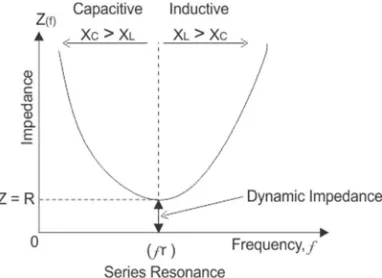
The impedance characteristics of a series resonant tank is as shown in Figure 2.6.
Hence, it acts like a filter for the switching frequency component of the current and power transfer
happens through the fundamental component of the current. Thus, we can analyze the circuit
considering only the fundamental component of the various signals. This is known as the
Fundamental Harmonic Approximation (FHA) and gives a sufficiently accurate model to allow us
to design the converter.
In order to obtain the DC gain of the resonant tank, the equivalent circuit shown in Figure 2.7 can
be considered.
Here, Req is the load resistance referred from the DC side to AC side of the rectifier and then, from
secondary side of the transformer to the primary side:
= 8 ∗ ∗ (2.1)
Figure 2.6 Impedance curve for series resonant tank Source: https://www.electrical4u.com/resonance-in-series-rlc-circuit/
Where,
n = Np/Ns (Primary turns/Secondary turns)
RL = load resistance
The above circuit can be solved for the resonant tank gain to get the following expression:
( , , ) = ( )
( )
= ∗
((1 + ) ∗ − 1) + ( ∗ ( − 1) ∗ ∗ )
(2.2)
Where,
= 1
2 ∗ ∗
fn = fS/f0 = normalized switching frequency
= 1 ∗
m = Lm/Lr
It can be observed from the above gain equation that it depends on the normalized switching
frequency along with two parameters: the tank Q-factor and the ratio of the magnetizing to the
resonant inductance, m. Based on these two parameters, we can compute the tank component
values, Lr, Cr and Lm. Thus, a design methodology needs to be outlined to decide the two
2.2.1 Design Methodology
The first step is to decide the turns-ratio for the transformer. There can be different ways to design
this parameter. The turns-ratio decides the gain requirement of the resonant tank, based on the
range of input voltages. One of the ways is to decide the turns-ratio based on the nominal input
and output voltages since, this would lead to the converter operating at resonant frequency (best
efficiency of operation) at the nominal operating voltages. Since, the converter is expected to
operate most of the time at nominal conditions, this selection of turns-ratio leads to improved
energy-efficiency. The specifications for the converter prototype developed in this thesis are given
in Table 2.1.
The second step in the design procedure is to decide the gain requirement from the resonant tank
based on the output voltage and input voltage range of regulation. Based on the specs, the gain
requirement of the resonant tank is as follows:
Table2.1 Converter prototype specifications
Parameter Target Value
Input Voltage 250-280 V
Output Voltage 28 V (Nom.)
Max. Load Power 1 kW
Switching Frequency >100kHz
Output Voltage ripple (pk-pk) <1.5 V
Efficiency > 97%
Power density 5kW/L
Minimum Gain (at Vin =280V) = 270/280 = 0.964
Maximum Gain (at Vin =250V) = 270/250 = 1.08
However, we need to keep some margin in the peak gain to allow operation in the inductive region
during transient conditions. Keeping a margin of nearly 20% in the peak gain, we get a maximum
the peak gain is the maximum load conditions. Hence, we need to ensure that the maximum gain
requirement is met at maximum load conditions i.e. at Qmax.
The third step in the design procedure is to decide the values for Qmax and m. It is important to
understand the qualitative effect of the two parameters to be able to decide on optimal values of
the two.
Higher Qmax leads to a tighter frequency range of regulation since the minimum gain is achieved
with less increase in frequency. However, a higher Qmax limits the peak gain in which case, the
peak gain requirement might not be met. A lower Qmax might be able to achieve the peak gain
requirement, but is less sensitive to frequency modulation in the region above resonance frequency.
A lower m might be able to meet the gain requirement. However, this means a reduced Lm which
leads to higher circulating currents and conduction losses, which affects converter efficiency
drastically, especially at light loads. Also, a lower m also leads to steep gain curves, which means
a large gain variation for a small change in frequency. This can cause issues in digital
implementations of control which are limited by the resolution of the controller platform being
used for the implementation. A higher m is better from the point of view of efficiency, due to lower
magnetizing circulating current. However, the peak gain reduces with increasing value of m.
We can plot the peak gain vs Qmax at different values of m, as shown in Figure 2.8. Also marked
in the Figure is the max gain requirement, including the safety margin. This will allow us to get a
few combinations of Qmax and m which can meet the gain requirements. Thus, we have a sample
Figure 2.8 Plot of peak gain vs Qmax for different values of m
A common range for the value of m is between 4 and 10. As a starting point, a moderate value of
Qmax i.e. close to 0.5 is reasonable. Considering the different combinations in the sample space and
with a range of Qmax and m in mind, we can narrow down to a few designs, shown in Table 2.2.
For each of the selected designs, we compute a few parameters such as the minimum and maximum
frequency of operation over the input voltage range and the load range, resonant tank component
values i.e. Lr, Cr and Lm. Note that the values mentioned here are based on a resonant second
resonant frequency of 200kHz, decided according to the specifications in Table 2.2. The target is
to minimize the frequency range of operation (since it allows for better regulation along with
ensuring a lower size of magnetics, being dictated by the minimum frequency of operation though,
this effect may not be very pronounced) and the maximize the magnetizing inductance (since it
results in lower circulating currents and hence, boosts efficiency at light loads).
Table2.2 Frequency range of operation, Peak magnetizing current and resonant tank parameter values for different designs under consideration
Qmax m(=Lm/Lr) fmin fmax Δf Lr Lm Cr Impeak
Design I 0.44 5 166kHz 220kHz 54kHz 20.7µH 103.45µH 30.6nF 3.2A
Design II 0.47 4.5 170kHz 218kHz 48kHz 22.1µH 99.45µH 28.65nF 3.39A
Based on the above target, the selected design is highlighted in the Table 2.2. Note that the selected
design has a very narrow range of frequency for operation, compromising a little on the
magnetizing inductance, Lm. This is based on the peak magnetizing current computation for the
three design cases, shown in the last column of Table 2.2. The increase in magnetizing current in
design III is nearly 12% with respect to design I whereas the reduction in the range of operating
frequency is nearly 28%.
This completes the design of the converter. One more important component to be designed is the
output capacitor value. It is not only important from the perspective of the voltage ripple but also
CHAPTER 3 SMALL-SIGNAL MODELLING AND CONTROLLER DESIGN
The various loads in an electric vehicle such as electronic loads, air-conditioning loads, etc. require
a well-regulated supply for their operation. However, the operating profile of the loads are varied.
To ensure a stable regulation at all load and input voltage conditions, the controller must be
designed considering the model of the converter system at the various operating conditions.
Usually, an averaged model is enough for the control design. However, such a modelling approach
is not valid for resonant converters since, some of the state variables do not have DC components
but have strong switching frequency components and its harmonics. Due to the strong oscillatory
nature of the states, the switching frequency interacts with the natural resonant frequency of the
system which results in the phenomena of beat-frequency dynamics. Different methods have been
proposed in literature [2-5, 7] for modelling of resonant converters. One of the most successful
models is the extended describing function method. This method is discussed further in this chapter
to derive the equivalent circuit model. This model is then utilized to design the feedback network
for stable regulation.
3.1 Extended Describing Function Method
The first step towards modelling the LLC resonant converter is to describe the converter as a set
of non-linear state equations using Kirchhoff’s Laws. The non-linear or quasi-sinusoidal terms are
represented as by their harmonic components as the next step. Usually, the order of the harmonics
is restricted to the first harmonic component. This step of representing the non-linear terms with
their harmonic components is termed as the Extended Describing Function (EDF) method. The
following analysis uses only the first harmonic component for simplicity. The current and voltage
of the output filter are approximated with their DC components. The next step is to plug in the
out the DC, sine and cosine components. The sine and cosine circuits are together represented in
the form of a large signal model which is then perturbed and linearized to obtain the small-signal
model of the converter.
The procedure outlined above is used as follows. The detailed derivation is provided in [2] and is
reproduced here for convenience of the reader, with some modifications to take into account the
full bridge converter for generating the input pulses for the resonant tank, instead of the half-bridge
converter considered in [2].
Figure 3.1 Equivalent circuit of LLC resonant converter
Based on the equivalent circuit shown in Figure 3.1, we can write the following equations:
Where,
sgn(ip) = +1, if V’cf ≥ 0 −1, if V’cf < 0
=
=
= + + = 1 + +
(3.2)
(3.3)
(3.4)
= + ( )
(3.5)
The quasi-sinusoidal terms in the above equations can be approximated with their harmonic
components as part of the next step. Here, only the fundamental harmonic is used to represent the
following terms:
Similarly, the non-linear components can be expressed as:
( ) = ( ) sin( )
= , , sin( ) − , , cos( )
= ( , )
(3.7)
Where,
( ) = 4
, , = 4 =
, , = 4 =
= +
Where,
, =
( ) = ( ) ( ) − ( ) ( )
( ) = ( ) ( ) − ( ) ( )
( ) = ( ) ( ) − ( ) ( )
=
, =
=
, =
= /
Plugging the above harmonic approximations, equations (3.6)- (3.7) in the non-linear equations of
the system, equations (3.1)-(3.5), we can separate the DC, sine and cosine terms to get separate
circuits, representing the large signal model of the LLC resonant converter, as shown in Figure
3.2.
Figure 3.2 Large-signal model of LLC resonant converter
Using the large-signal model shown in Figure 3.2, we can get equations for the steady-state
operation. The small-signal model can then be obtained by perturbing and linearizing the
Steady-state operating point:
Filter cap voltage, Vcf:
= 2 =2
=2 =
4
= 4
(3.8)
Where,
= 8 =
Sine circuit:
= 4 = + + + = ( + ) − + +
=
= = ( − )
(3.9)
Cosine circuit:
0 = − + + = ( + ) − − +
= −
− = = ( − )
(3.10)
Thus, the steady-state operating point for the various state variables can be found by solving the
following matrix equation (3.11):
⎣ ⎢ ⎢ ⎢ ⎢ ⎡ ⎦ ⎥ ⎥ ⎥ ⎥ ⎤ = ⎝ ⎜ ⎜ ⎛ ⎣ ⎢ ⎢ ⎢ ⎢
⎡( + ) 1
− ( + ) 0
1 0 0
0 1
0 0
0 0
0 − 0
1 0 −
− 0 0
0 0 0
0 − −
0 − ⎦
The next step is to perturb the state variables (both sine and cosine components), input, output
and control signals. The perturbed signals are as follows:
= + , = + , = + , = + , = +
= + , = + , = + , = + , = +
= + , = + , = + , = + , = + , = +
(3.12)
Plugging the perturbed signals above to the large-signal equations and linearizing, we get the
following small signal model. For details about the linearization, please refer [2].
= + = + (3.13) Where, = [ ] = = [ ] = ℎ = ⎣ ⎢ ⎢ ⎢ ⎢ ⎢ ⎢ ⎢ ⎢ ⎢ ⎢ ⎢ ⎢ ⎢ ⎢ ⎢
⎡ −( + ) −( + ) − 1 0 −
( − )
−( + ) 0 − 1 −
1
0 0 − 0 0 0
0 1 0 0 0 0
0 0 − −( + )
0 0 −( + ) −
0 0 − − −
= −( ) ( ) −( ) ( ) −( ) ( ) 0
= 0 0 − −
= [0]
Where,
=4
= −4
= 4
= −4
= 4
=4
= 4sin ( 4)
= 2 cos (
4)
= 2
+
=2
+
Thus, based on the above equation, we can solve for the control (ωsn) to output (vo) transfer
order transfer function as shown below. This can then be used to design the closed loop control for
the converter. It must be noted that the above equations are for a 50% duty cycle of the applied
voltage and for a full-bridge converter at the primary-side of the transformer. Some of the terms
will need to be modified in case the duty cycle is also varied or if the converter at the primary-side
of the transformer is a half-bridge.
For the design parameters selected in Chapter 2, the control to output transfer function at 50%
load is computed as below. Note that this is the reduced-order transfer function.
( )
= 3.2266 ∗ 10 ( + 2.6849 ∗ 10 )( − 2.4197 ∗ 10 )
( + 2.4992 ∗ 10 + 64.07424 ∗ 10 )( + 0.1116 ∗ 10 + 2.00845 ∗ 10 )
(3.14)
Figure 3.3 Bode plot for converter control-to-output transfer function (@Vin = 270V, Pload = 500W)
The bode plot corresponding to this transfer function is shown in Figure 3.3. We can observe a
few important points from this. First, the system has the presence of one right-half plane zero at
385 kHz. Since, this is much beyond our resonant frequency and hence, the range of switching
frequencies, it will not affect the Phase Margin of the control loop. Second, the system has two
complex double poles. The dominant complex double pole represents the beat frequency dynamics
switching frequency becomes closer to the resonant frequency, one of the beat frequency pole
moves to lower frequencies and forms a double pole with the output filter pole. This is the case in
the transfer function shown above. Thus, as the output capacitor value is increased, this double
pole frequency moves to lower frequencies. Moreover, the double pole is damped by the equivalent
load resistance. Higher the load, greater is the damping provided to the dominant complex double
pole.
Now that we have the control to output transfer function, we can design the closed-loop control
for the converter. Different control strategies have been applied in literature [8-11]. However,
variable frequency control is the most commonly used strategy.
3.2 Controller Design
To ensure stability of the controller at all operating conditions, it is necessary to decide the
worst-case conditions for the design. These are the conditions under which the Phase-Margin and
gain-Margins can be reduced. At the double pole frequency, the phase-drop is steep. The slope of the
phase-drop depends on the damping at the double-pole frequency. Hence, the worst-case scenarios
are the cases for minimum input voltage (lowest frequency range of operation), maximum and
minimum load, as well as maximum input voltage (highest frequency range of operation). Ensuring
adequate phase margin and gain margin in all these cases can ensure stable operation at all
operating conditions.
When designing the controller for a particular system, we need to decide the required cross-over
frequency based on the desired transient response. While designing the converter prototype, we
had not been provided with any transient specifications. However, it is desirable to reduce the
effect of any disturbance, either in the input voltage or load, as seen in the output voltage. This
less than 0dB at all frequencies. In case the magnitude of the transfer function goes above 0dB for
any frequency, we can observe ringing in the output response at the same frequency, for a step
disturbance to the system. For a closed loop system, the transfer function from the output voltage
to disturbance is reduced by the loop-gain below the cross-over frequency. On plotting the output
impedance of the converter, we observe that the response has a steep increase in impedance at the
double pole frequency. In order to reduce the effect of a step change in load, we must ensure that
the cross-over frequency is above the double pole frequency. Note that even when the double-pole
frequency is below the cross-over, the effect of the double pole can be seen as an oscillation in the
output for a step disturbance in load, though the amplitude of the oscillation will be reduced due
to the attenuation by the loop gain. This can be observed in Figure 3.4(b).
As a general design practice for PWM converters, the cross-over is usually selected between 1/10
to 1/5 of the switching frequency. Following a similar design approach in case of the LLC resonant
converter, we can decide for a cross-over frequency of say, 20-30 kHz (1/10 of resonant
frequency). This means that the pole frequency must be below 20 kHz. Since, the
double-pole frequency is decided by the equivalent resonant inductance and the reflected output
capacitance, it implies a large output capacitor. This is a limitation in many cases where size is a
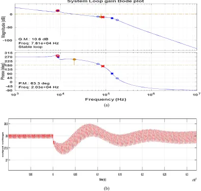
major constraint. Such a design is illustrated in Figure 3.4 for a 470µF output capacitor along with
(a)
(b)
Figure 3.4 (a) Loop-gain bode plot for converter design with output capacitor of 470µF and cross-over frequency beyond double pole frequency. (PM: 63.3 deg, GM: 10.6dB, cross-over: 20.3 kHz) (b) Simulation results for step change in load from 30% to
100% @ Vin=270V (undershoot: 0.5V, settling time: 100µs)
Another limitation to this implementation comes from the digital implementation of the controller.
It must be ensured that the sampling frequency for the output voltage is at least 10 times higher
than cross-over frequency to ensure that the phase margin at cross-over is not affected by the
sampling. However, in many cases, the sampling can get limited due to the computation time
requirement for the control implementation. It is due to these two constraints that the control
bandwidth for the prototype implementation has been designed to be below the complex
double-pole frequency. Note that the value of output capacitor has been reduced in this case to 72µF based
3.5 and the achieved phase margins and gain margins for the corner cases mentioned above, are
provided in Table 3.1.
One important point to keep in mind while designing the controller is to ensure that the magnitude
plot of the loop gain does not have a second 0dB cross-over, which is possible at the dominant
complex double-pole frequency. Such a scenario can lead to a conditionally stable system i.e. the
system can become unstable with changes in the operating point or with disturbances of
sufficiently large amplitude. In the bode plot shown in Figure 3.5, the double pole is 32.9dB below
the 0dB line.
Table 3.1 Loop gain parameters for the designed controller for the four corner cases
Max. Vin (280V),
High load (1kW)
Max. Vin (280V),
light load (0.3kW)
Min. Vin (280V),
High load (1kW)
Min. Vin (280V), light
load (0.3kW)
Gain Margin 31.3 dB 35.4 dB 30.9 dB 32.9 dB
Phase Margin 88.7 deg 89.4 deg 86.8 deg 88.6 deg
fcross 1.08 kHz 0.983 kHz 1.39 kHz 1.67 kHz
The control architecture used here is a two-zero, three-pole structure, consisting of one complex
zero, one complex pole and an integrator. The complex zero and pole combination forms a
complex lead-compensator. This is used here to reduce the overshoots caused by the double-pole
and also, to compensate for the associated steep phase drop. This structure has a disadvantage from
the perspective of sensor noise attenuation. The bode plot of a complex lead compensator is shown
in Figure 3.6 [6]. It has an increased high-frequency gain, which can amplify any noise coming
from the output voltage sensing, which can then be reflected in the output voltage. Hence, it is
important to ensure low noise in the sense circuitry.
Figure 3.6 Bode plot of a complex lead compensator (damping constant: 0.707)
3.3 Discretization and Digital Controller Implementation
Digital implementation of a controller is often preferred over analog implementation due to greater
flexibility, elimination of dependence on component tolerance, ability to implement complex
control algorithms, reduced interference due to signal noise. However, it is dependent on sampling
a continuous time system and performing control computations on the samples. Sampling a
continuous time system changes the model of the system based on the rate of sampling. There are
be to design the controller based on the continuous time model of the system and then discretize
the controller by expressing it as a combination of integrators and using a discrete approximation
such as backward Euler, forward Euler or Tustin approximation. The second approach is to
discretize the model of the system, using any of the above mentioned approximations and then
design the controller based on the discretized model. This approach is useful for systems which
have second-order effects at frequencies close to the sampling frequency of the system. Sampling
a continuous time system has a secondary effect called aliasing. As an example, a high frequency
double pole beyond half of the sampling frequency (Nyquist frequency) is aliased to a lower
frequency and can have an effect of reducing the phase margin of the control loop at cross-over
frequency, in case the cross-over is less than a decade away from the aliased double pole frequency.
Hence, this effect must be considered during control design, for cases where the sampling
frequency is close to ten times the cross-over frequency and the system model reveals presence of
second order effects close to the sampling frequency. Thus, the second approach to controller
design can allow a more accurate controller design compared to the first approach. This is used for
designing the controller in this work, even though the cross-over frequency has been limited to
nearly 1.6 kHz.
For the discretization of the system, Tustin approximation is used here since it has a 90 deg phase
lag characteristics for an integrator till the sampling frequency whereas the phase characteristics
for backward and forward Euler diverge away from 90 deg lag as we move closer to the sampling
frequency. This becomes more important as the sampling frequency moves closer to the
cross-over frequency. In the present case, the sampling frequency is equal to the switching frequency
(175 kHz – 215 kHz), which is much higher than the cross-over frequency (1.6 kHz) and hence,
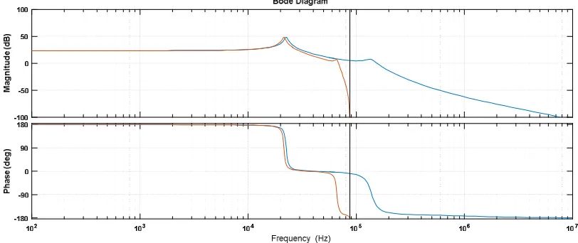
The discretized model of the converter is shown in Figure 3.6 for Vin = 250V, light load (0.3 kW).
Also plotted on the same plot is the bode plot of the continuous domain model. The sampling
frequency used in this case is 175 kHz. The bode plot of the system loop gain, including the
controller designed based on this discretized model is shown in Figure 3.7.
Figure 3.7 Discretized model of the converter system using Tustin approximation (sampling frequency: 175 kHz) along with continuous domain model
This controller is implemented in a Digital Signal Processor by converting the ‘z’ terms in the
controller to ‘z-1’ and forming a difference equation, where each ‘z-1’ term means a delay of one
sample. The hardware results based on this designed controller are presented in a later chapter.
CHAPTER 4 SYNCHRONOUS RECTIFICATION
The LLC resonant converter, being a soft switched converter, is able to reduce the switching loss
to being nearly negligible. However, conduction losses are not mitigated. A major contribution to
the total device losses comes from the diode conduction in the secondary side rectifier where a
current which is much higher than the primary-side (due to the high step down ratios usually
present with these converters) conducts through a diode. This diode is often replaced with a device.
In order to reduce these conduction losses, the device can be turned-on synchronously with the
diode conduction. This means the channel of the device conducts the current, leading to the losses
being the I2R losses, which are usually much lower than the V
F*I losses in the diode. This helps improve the efficiency of the converter.
In order to further reduce the losses, efforts have been made to reduce the RDS(ON) of the device.
With the introduction of Wide-Band Gap (WBG) devices based on GaN and SiC, a significant
reduction in RDS(ON) has been observed. Hence, for the current prototype, GaN based devices have
been used for both the primary and secondary side of the converter.
With the use of GaN devices, an issue which arises is the increase in reverse conduction drop due
to the negative voltage used during turn-off (for noise immunity at the gate terminal due to high
dv/dt), being added to the threshold voltage during reverse conduction. This means that
synchronous rectification becomes a requirement due to thermal considerations. Moreover, with
the reduced size of the devices, thermal management becomes very difficult. This points towards
a need to optimize the synchronous rectification pulse duration, to minimize the period of reverse
One of the main challenges to synchronous rectification in the LLC resonant converter arises for
operation below resonant frequency. In this region of operation, the diode current falls to zero
before the end of the switching half period. The synchronous rectification pulse must be withdrawn
before the diode current falls to zero. In case the device is allowed to conduct beyond this instant,
it can allow a current to flow in the reverse direction, meaning that the output capacitor is
discharged. This leads to additional losses in the device and can also lead to instability in the
designed controller. Thus, the SR pulse turn-on can be synchronized with the primary pulses with
some constant delay whereas the turn-off needs to be tuned based on an algorithm.
Many methods of active synchronous rectification have been proposed in literature [12-16], based
on sensing the tank current or sensing the secondary device Vds. Many ICs are present in the
market, which depend on sensing the device Vds to optimize the synchronous rectification pulse.
A digital implementation of synchronous rectification based on Vds sense was proposed in [12].
This method has been used in the current prototype.
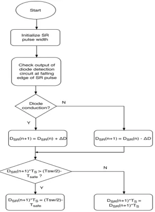
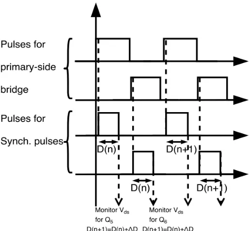
4.1 Digital Implementation Algorithm
The method detailed below is proposed in [12]. It is based on a diode conduction detection circuit,
shown in Figure 4.1. When the diode of Q5 is conducting, the drain of Q5 is at a lower potential
than the source node, which is the ground reference for the secondary-side circuits. This causes
the diode D1 to become forward biased and the potential at the inverting terminal of the comparator
becomes equal to the drain voltage of Q5 + the forward drop of diode D1.This is compared with a
the device. This causes the output of the comparator to be latched high when the diode starts
conducting. The output of the comparator can then be taken to a digital signal processor (DSP)
using a digital isolator, to ensure isolation between the power ground and the DSP ground.
The algorithm used to optimize the synchronous rectification pulse widths using the pulses from
the circuit in Figure 4.1, is shown in Figure 4.2. In the beginning, a fixed pulse width is used for
the synchronous rectification pulses. The pulses from the diode conduction detection circuit are
taken to a GPIO on the DSP, the state of which is monitored at the falling edge of the synchronous
rectification pulses. If a high is detected, it means that there is diode conduction, in which case,
the pulse width is incremented by a small value ∆t, which should correspond to the minimum
resolution of the controller platform used. If a low is detected, it implies lack of diode conduction,
in which case, we need to reduce the pulse width, since we have gone beyond the desired diode
conduction duration.
Figure 4.2 Synchronous rectification algorithm flow chart
Towards the end of the diode conduction period i.e. at the instant when the load component of tank
current equals the magnetizing current, we shall observe a jitter, merely due to the logic of the
algorithm. The duration of this jitter is equal to the duration of increment, ∆t. It is desirable to keep
this jitter at minimum, to avoid going beyond the desired diode conduction period since this can
lead to circulating currents in the secondary due to the device being turned on even after the current
platforms. As ∆t increases, it can increase the duration for which the switch allows the negative
current to flow, which can cause the control to become unstable. This can be a major drawback of
this approach.
Moreover, the optimal pulse width is achieved after a large number of cycles since we want ∆t to
be small. Hence, this method can have poor transient performance.
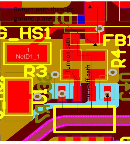
4.2 Layout Recommendation
One important point to be considered during the layout of the diode conduction detection circuit
in the above algorithm is to ensure that the drain connection and the corresponding return
connections are routed as kelvin connections, i.e. the drain connection for this circuit is routed
directly from the drain of the device (path 1 in Figure 4.3) rather than branching out from the
power circuit drain connection (path 2 in Figure 4.3). This is to reduce the interference
Figure 4.3 Layout recommendation for Diode conduction detection circuit. Path 1 should be used for forward path with kelvin connected return path overlapped with forward path
between the power circuit and the Vds sense circuit so that it does not lead to false trigger of the
4.3 Implementation on TI-TMS320F28335
The algorithm for Synchronous rectification using Vds sense detailed above has been implemented
on TI-TMS320F28335. Two EPWM channels are used for generating the SR pulses. The counter
for these channels are synchronized to the primary-side EPWM channel and a rising edge delay is
provided using the DB module. The initial pulse-width is kept equal to one third of the resonant
period. The two channels are 180 deg. Phase shifted from each other. The generated pulses are fed
back to two GPIO pins which are designated for external interrupt at the falling edge. The Vds
sense pulses are fed to two other GPIO pins which are monitored inside the respective interrupts
generated by the external triggers.
CHAPTER 5 HARDWARE IMPLEMENTATION AND RESULTS
A prototype of the LLC resonant converter was developed in the laboratory. This prototype has
an H-Bridge to generate the pulses to be applied to the resonant tank. As mentioned in Chapter 2,
this helps reduce the device conduction losses on the primary side to half of the value compared
to a half-bridge. The devices used for this H-Bridge are the GaN Systems GS66516T. These
devices are rated for 650V, 60A (@25ºC) and 47A (@100ºC). The current rating for this device
is much higher than required. However, the on-state resistance is very low, of the order of 25mΩ.
This further helps to reduce the conduction losses on the primary side.
The secondary side rectification is using a center-tap transformer and two devices. This also
helps to reduce the secondary-side conduction losses to half of the value achievable for
full-bridge rectification. Moreover, it is preferable over full full-bridge rectification in cases where the
output voltage is low since we have voltage drop from a single device instead of two devices in
full-bridge rectification.
Figure 5.1 Picture of the Hardware test setup for LLC resonant converter
The image for the hardware setup is shown in Figure 5.1. The PCB for the converter has the
equalize the parasitic inductance in the secondary terminals of the transformer, which helps
match the overshoots seen by the secondary devices. Second, as a future task for the project, it
shall be modified for bi-directional operation, which requires the secondary side to be replaced
by an H-Bridge. Hence, the daughter card design used here allows a modular design where the
secondary card can be modified based on the desired application. The next section describes the
specifics of the board layout.
5.1 Gate Drive Design
The gate drive design for the GaN devices used in the prototype is shown in Figure 5.2. The Figure
highlights the turn-on and turn-off path for the gate terminal of the device. The gate driver IC used
here is SI8271 [17]. This IC has a low UVLO (Under Voltage Lock-out) of 3V, high CMTI
(Common Mode Transient Immunity) of >200 kV/µs. Moreover, it has separate pins for the
turn-on and turn-off processes. This eliminates the need to use anti-parallel diodes to provide separate
turn-on and turn-off resistances.
Due to the high dv/dt of the GaN devices, the CGD of the devices sees the high dv/dt at the turn-on
of the complimentary device. This causes a current to flow through CGD which can charge the CGS
of the device and if it is charged above the threshold of the device (which is of the order of 1.1-1.3
V for the GaN devices under use), it can lead to false turn-on of the device and partial
shoot-through condition. In order to improve the gate immunity towards a false turn-on, negative gate
bias is used during turn-off. Moreover, a low gate resistance is used during turn-off, compared to
turn-on. This provides a parallel path for the CGD current and hence, reduces the charge pushed
through CGS of the device, preventing it from getting charged to the threshold. Also, due to the
current flowing through the CGD of the device, it provides an excitation to the parasitic inductance
of the gate loop and the input capacitance of the device. This is seen as a ringing in the gate of the
device during turn-off. In order to damp this ringing in the gate, a ferrite bead is added in the gate
path. This ferrite bead is a frequency dependent series RL component, which provides high
impedance at higher frequencies and hence, helps to damp the oscillations in the gate.
Another important point to be taken care of during the layout is to minimize the area of the gate
loop. A good design practice is to overlap the forward and return paths for the drain currents. This
causes flux cancellation between the two paths and hence, helps reduce the effective inductance
of the gate loop. Here, the return path is provided through an inner ground layer.
It must be noted that in case of the GaN devices used in this prototype, no kelvin connection has
been provided for the source terminal. Hence, it must be ensured that the source connection for the
gate loop is tapped from the nearest pin on the source pad, to the inner layer, where it is routed
separate from the power circuit source connection. This is extremely necessary otherwise, the
parasitic inductance common to the gate loop and power loop can increase. Since a high current is
voltage seen by the gate loop at the commutation instant. If this voltage is higher than the negative
bias by the threshold voltage, it can lead to false turn-on of the device. Hence, it must be ensured
that the source connection is made as a kelvin connection, even if one is not provided in the device.
5.2 Power Loop Design
The layout of the power loop has become very essential with the increased usage of Wide-Band
Gap (WBG) devices. Due to the high switching speeds of these devices, the operating di/dt can be
very high, especially for high current operation. This can lead to high voltage overshoots in the
device Vds at turn-off. Hence, it is preferable to minimize the power loop inductance, for better
device reliability.
One of the techniques used for power loop inductance is to place decoupling capacitors having
low ESL, right next to the top device. The high frequency switching currents required to charge
the output capacitors of the devices are provided by these decoupling capacitors and the path for
these currents have low inductance since they are placed very close to the devices. In the current
prototype, low-ESL ceramic capacitors from TDK Ceralink series is used for the decoupling. They
have a specified ESL of 2.5nH and four of these are used in parallel, reducing the effective parasitic
inductance to a very small value (<1nH).
Another important concept used to reduce the power loop inductance is that of flux cancellation
of the forward and return current carrying paths, when routed differentially. This can help reduce
the loop inductance. The above two ideas are combined in the current prototype for the primary
High-side devi ce Low-side device Decoupling capacitors
Commutation loop
Top Layer
Inner Layer I
Inner Layer II
Bottom Layer Commutation loop
Figure 5.3 Power Loop design for Primary-side H-Bridge
5.3 Parameter Measurement of Transformer and Inductor
The center-tapped transformer and inductor used for the prototype development are acquired from
Payton Planar magnetics. The reason for using a separate inductor for the resonant tank is that to
allow more accurate design for the value of the resonant inductor. Moreover, we need to reduce
the leakage on the secondary side to reduce overshoots in the device Vds, especially above resonant
frequency operation. Hence, the transformer was designed to have low leakage inductance and the
inductor was designed as per the required value of Lr.
To get a low leakage inductance, and also to get a better thermal performance, an interleaved
winding design was used for the transformer. Before using the transformer and inductor in the
circuit, we need to extract the parasitic elements of the same, which can then be used in the
utilized. The impedance curve for the inductor is shown in Figure 5.4. The parameters extracted
from the curve are given in Table 5.1.
Figure 5.4 Impedance plot for resonant inductor
Table 5.1 Measured parameters for the transformer and inductor used in the prototype
INDUCTOR PARAMETERS
Self-resonant frequency 9.28 MHz
Nominal inductance value (@ 250 kHz) 24.8µH
Effective parasitic capacitance 13 pF
Peak current rating 7.5 A
TRANSFORMER PARAMETERS
Magnetizing inductance 94 µH
Primary referred leakage inductance 0.62 µH
Primary referred intra-turn capacitance 150 pF
Inter-winding capacitance (between primary and secondary windings) (@ 250 kHz)
3 nF
For the transformer parameters, the secondary was kept open – circuited and the impedance at the
primary terminals was measured. This impedance curve is shown in Figure 5.5. Also, the nominal
inductance measured in the inductive region of the impedance curve, at 250 kHz, is equal to 94.6
µH. This corresponds to the magnetizing + the leakage inductance. Moreover, from the