ABSTRACT
REZAEI, MOHAMMAD ALI. Design, Implementation and Control of A High Efficiency Interleaved Flyback Micro-Inverter for Photovoltaic Applications. (Under supervision of Dr. Alex Q. Huang)
Photovoltaic (PV) micro inverters have been gaining attention for the grid-connected
PV systems because of improved energy harvest, friendly “Plug-N-Play” operation, and
enhanced modularity and flexibility. Various inverter topologies for PV micro-inverters
applications have been introduced in the literature that perform the maximum power point
tracking (MPPT) of PV module, high step-up voltage amplification, output current shaping,
and galvanic isolation. Among them, the flyback based micro-inverter is one of the most
attractive solutions due to its simple structure and control and also its inherent galvanic
isolation.
The conventional flyback micro-inverter consists of decoupling capacitor, interleaved
flyback converter, unfolding bridge, and CL filter. The unfolding bridge is switched at line
frequency by a simple square-wave control, generating a rectified sinusoidal waveform at the
dc-link between the interleaved flyback converter and unfolding bridge. The decoupling
capacitor maintains the power balance between the constant input power and variable output
power oscillating at double-line-frequency. All the other functionalities required in PV
micro-inverter are performed by the flyback converter. Therefore, the flyback converter has
been widely scrutinized to improve its performance in terms of efficiency, reliability, and
cost.
strategy controls the inverter in the Boundary Conduction Mode (BCM) in order to exploit
the natural resonance of the flyback transformer to achieve Zero Voltage Switching (ZVS)
during the turn-on process. At low load and near the zero-crossing of the grid voltage, the
switching frequency of the inverter is then limited by transitioning to Discontinuous
Conduction Mode (DCM) to limit the switching loss. Although this hybrid switching strategy
ensures the ZCS turn-on for every switching cycle and ZVS turn-on for most of the grid
cycle, it does not provide any mechanism to limit the turn-off switching loss, which is the
major source of loss in the flyback converter.
In order to limit the turn-off switching loss, a novel adaptive snubber is developed in
this thesis which ensures soft switching during the turn-off process. The developed adaptive
snubber requires the minimum number of components and operates only at double-line
frequency, which makes the control system easy and straight forward. Using the proposed
adaptive snubber technology, a maximum efficiency of 96% is achieved.
Based on the proposed adaptive snubber with the associated hybrid switching method,
the operation of the inverter is then further optimized in order to achieve the maximum CEC
efficiency. The presented efficiency optimization procedure accurately takes into account the
transformer and switching losses of the inverter and optimizes the parameters of the
hardware and controller. The optimized hardware achieves the CEC efficiency of 94.96%,
© Copyright 2015 Mohammad Ali Rezaei
Design, Implementation and Control of A High Efficiency Interleaved Flyback Micro-Inverter for Photovoltaic Applications.
by
Mohammad Ali Rezaei
A dissertation submitted to the Graduate Faculty of North Carolina State University
in partial fulfillment of the requirements for the Degree of
Doctor of Philosophy
Electrical Engineering
Raleigh, North Carolina 2015
APPROVED BY:
Dr. Srdjan Lukic Dr. Wensong Yu
DEDICATION To my wife:
Dr. Maedeh Heidarpourroushan
BIOGRAPHY
Mohammad Ali Rezaei was born in Esfahan, Iran. He received his B.Sc. and M.Sc.
degrees in electrical engineering from University of Tehran, Tehran, Iran in 2008 and 2011
respectively. In fall 2011, he joined the Future Renewable Electric Energy Delivery and
Management (FREEDM) Systems Center of North Carolina State University, Raleigh, to
pursue his Ph.D. degree. His main research interests is in the area of power electronics
including: digital control of power converters, high frequency DC-DC converters, application
of GaN and SiC devices in power electronics and power electronics for renewable energy
ACKNOWLEDGMENTS
I would like to express my deepest gratitude to my Ph.D. adviser and mentor,
Professor Alex Q. Huang for all his guidance and support. During my research work at the
FREEDM Systems Center, I have benefited tremendously from his knowledge, creative
thinking and professional insight. I feel blessed to have such a great scholar with such a
warm character as my mentor.
I also would like to extend my gratitude to Dr. Wensong Yu, Dr. Srdjan Lukic and
Dr. Robert Riehn for serving on my committee and their feedback and support.
I also would like to thank our lab manager in the FREEDM System Center, Mr.
Hulgize Kassa and his assistant, Mr. Gregory Norris for all their efforts in maintaining and
handling lab equipment and providing us with a safe environment.
My gratitude also goes to all members of FREEDM Systems Center, specially, Dr.
Kuijun Lee, Dr. Ruiyang Yu, Dr. Gangyao Wang, Dr. Fei Wang, Md. Tanvir Arafat Khan,
Elie Najm, Qingyun Huang, Yan-Ting Lee and many others that I cannot list their names
TABLE OF CONTENTS
LIST OF TABLES ... vii
LIST OF FIGURES ... viii
1. Introduction and Background ... 1
1.1 Introduction ... 1
1.1.1 Background and motivation ... 1
1.1.2 PV inverters ... 4
1.2 Inverter topologies for ac-module application ... 10
1.2.1 Topologies with ac-dc link ... 11
1.2.2 Topologies with pseudo dc link ... 14
1.2.3 Topologies without dc-link ... 18
1.3 Selecting the suitable topology for residential applications ... 20
1.3.1 Flyback micro-inverter ... 21
1.4 Presented innovative approaches in this thesis ... 24
2. Inverter Stage Innovation ... 26
2.1 Introduction ... 26
1.1 Innovative IFMI ... 27
1.1.1 IFMI mode of conduction ... 28
1.1.2 Innovative adaptive snubber ... 30
3. Design and Implementation of IFMI... 42
3.1 Design of the System Components... 42
3.1.1 Electrolytic capacitors ... 42
3.1.2 Primary and snubber MOSFETs ... 45
3.1.3 Flyback transformer core type and material ... 46
3.1.4 Magnetizing inductance value ... 50
3.1.5 Snubber capacitor Cs ... 51
3.1.6 Auxiliary switch ... 56
3.2 Experimental Results ... 57
4. Optimization ... 66
4.1 Introduction to the optimization process for the IFMI ... 66
4.2 IFMI loss modeling in MATLAB ... 68
4.2.1 IFMI transformer loss calculation ... 70
4.2.2 Filter capacitor loss calculation ... 72
4.3 Optimization procedure ... 73
4.3.1 Optimization results... 79
4.3.2 Experimental results ... 82
4.4 Comparison to available commercial products ... 84
4.4.1 Enphase M250 micro-inverter ... 84
4.4.2 Lead Solar LS250 micro inverter ... 85
4.4.3 Solar Bridge Pantheon P250LV-208/240 micro-inverter ... 86
5.1 Conclusion ... 87
5.2 Future work ... 88
REFERENCES ... 89
APPENDICES ... 94
LIST OF TABLES
Table 1.1: Brief summary of requirements of different standards for grid connected PV
systems ... 6
Table 1.2: comparison of ac-modules with dc-link ... 13
Table 1.3: comparison of topologies with pseudo dc-link ... 17
Table 1.4: several key parameters of micro-inverter without dc link. ... 19
Table 2.1: basic design specifications ... 27
Table 3.1: Specifications and ratings of the experimental setup ... 58
Table 3.2: list of major components in the hardware setup. ... 59
Table 4.1: Fixed parameters for the optimization procedure. ... 77
Table 4.2: Results of optimization for individual power levels in the CEC formula ... 79
LIST OF FIGURES
Fig. 1.1: Cumulative installed grid connected and off-grid PV power in reported
countries between 1992 and 2011 ... 2
Fig. 1.2: Average cost of silicon PV modules from 1976 to 2009 in comparison with average price of onshore wind farms. ... 3
Fig. 1.3: Photovoltaic system technologies. A) Past centralized technology, b) Present string technology, c) Present multi-string technology, d) Latest AC-Module technology. ... 5
Fig. 1.4: general form of ac-modules with a dc link. ... 11
Fig. 1.5: Topologies with dc-link ... 12
Fig. 1.6: general form of an ac-module topology with pseudo dc link ... 12
Fig. 1.7: Topologies with pseudo dc-link configuration. ... 15
Fig. 1.8: Topologies with pseudo dc-link configuration, continued. ... 16
Fig. 1.9: Topologies without dc-link. ... 18
Fig. 1.10: general form of an ac-module topology without dc link ... 18
Fig. 1.11: Conventional active clamping circuit in flyback micro-inverter ... 22
Fig. 1.12: Main operation waveforms of the active clamp circuit with non-complementary gate drive signal. ... 23
Fig. 2.1: Basic configuration of an interleaved flyback micro-inverter. ... 28
Fig. 2.2: Circuit configuration of the proposed adaptive snubber scheme in flyback micro-inverter. ... 31
Fig. 2.3: Main operation waveforms of the flyback inverter with the proposed adaptive snubber... 32
Fig. 2.4: Theoretical operation waveforms under BCM. ... 33
Fig. 2.5: Equivalent circuits for each operational mode: (a) Mode 1 [t0-t1]. (b) Mode 2 [t1-t2]. (c) Mode 3 [t2-t3]. (d) Mode 4 [t3-t4]. (e) Mode 5 [t4-t5]. ... 38
Fig. 2.6: average output current during the BCM operation ... 39
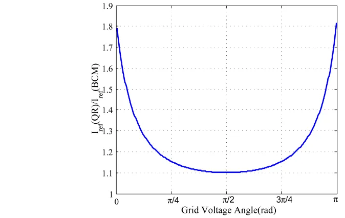
Fig. 2.7: Reference current considering FDCM=100kHz, N=6, Po=250W, Vo=240V, Ltot=6µH and Ctot=10nF. Comparison between DCM, ideal BCM and BCM considering tQR.in mode 4 ... 40
Fig. 3.1: Performance factor versus frequency for EPCOS core materials measured at
T=100˚C and Pv = 300kW/m3 ... 48
Fig. 3.2: comparison of power loss in three different core materials ... 49
Fig. 3.3: Minimum value of switching frequency in BCM versus magnetizing inductance for maximum power of 250 W in a 240V system. ... 50
Fig. 3.4: Peak voltage across the main switch for different leakage inductance values at grid angle = π/2 and for Po =250 W, vin =30.6 V, vo =240 Vrms, N =6, and Lm =6 uH. ... 52
Fig. 3.5: Peak voltage across the main switch for Ctot = 10 (nF).and for Po =250 W, vin =30.6 V, vo =240 Vrms, N =6, and Lm =6 uH. ... 53
Fig. 3.6: Equivalent circuit of the flyback converter during the turn off resonant period. ... 54
Fig. 3.7: Equivalent circuit of the impedance measurement test setup... 54
Fig. 3.8: picture of the hardware setup for measuring the impedance of the transformer primary ... 55
Fig. 3.9: Measured frequency response of the transformer’s primary winding. ... 56
Fig. 3.10: Photograph of the experimental prototype. ... 57
Fig. 3.11: control block diagram of the flyback micro-inverter. ... 60
Fig. 3.12: Experimental waveforms of grid voltage vg, grid current ig, gate-to-source voltage of the main switch S1, and gate-to-source voltage of the auxiliary switch Sa1. ... 61
Fig. 3.13: experimental waveforms of grid voltage vg, grid current ig, drain-to-source voltage of S1vds1, and primary side current of the transformer ip1. ... 61
Fig. 3.14L Interleaved operation during BCM. ... 62
Fig. 3.15: Operation Waveforms in BCM. ... 62
Fig. 3.16: Operation waveforms in BCM. ... 63
Fig. 3.17: Operation waveform during mode transition between DCM and BCM. ... 63
Fig. 3.18: Efficiency curve. ... 64
Fig. 4.1: Magnetic flux of a flyback transformer in the DCM operation. ... 71
Fig. 4.2: Schematics of IFMI (one phase) and magnetizing current reference. The free design parameters are shown in this figure in red. ... 74
Fig. 4.3: Flyback transformer winding structure ... 76
1.
Introduction and Background
1.1
Introduction
This chapter is an introduction on the Photovoltaic (PV) renewable energy systems.
We explain different parts of such systems and demonstrate why the “PV inverter” is one of
their most important parts. At the end of this chapter, we should be able to answer the
following important questions regarding the PV energy and PV inverter systems:
Why PV energy is important in the world of fossil fuels and nuclear energy?
What are the different types of PV inverter systems for residential and commercial
applications?
Why PV micro-inverter is an interesting solution for residential applications?
What is the aim of the current research work?
What is the impact of presented research work on the PV systems?
1.1.1 Background and motivation
The increasing concerns about the fossil fuel reserves and the environmental issues of
burning them have led the renewable energies to become the perspective of the power
generation. As the increasing power demand restricts the planning and installation of large
centralized power units, distributed renewable energy generation units are increasingly used
Among different types of renewable energy sources, photovoltaic (PV) energy is
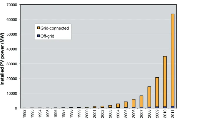
becoming more and more popular. As it is reported in [1] and illustrated in Fig. 1.1, the
cumulative installed grid connected and off-grid PV power in the reported countries has
increased from essentially zero, in 1992, to more than 63 GW in 2011. The downward
tendency in the price of PV modules due to massive increase in production capacity has
played a major role in this increase.
Fig. 1.2 illustrates the cost of PV modules over the year span of 1976 to 2009 in
comparison with the cost onshore wind farms. The gradual decrease in the cost of PV
modules is visible in this figure whereas the cost of wind farms has stayed almost the same
during this period.
In addition to reduced price, the durability of PV modules is an important factor in
popularity of PV energy. A PV module does not contain any moving parts, as opposed to Fig. 1.1: Cumulative installed grid connected and off-grid PV power in reported countries between
some of the other renewable energy sources such as wind. A long lifetime is therefore
guaranteed, without almost any tear-and-wear and maintenance. For example, Isofoton offers
a 10 year warranty on products and 30 years linear output power warranty [2].
As the cost of PV module decreases year by year, the cost of inverters is becoming
more visible in the total cost of the PV systems. It is worth mentioning that in addition to the
cost of inverter itself, installation of the inverter plays a major role in the total cost of the PV
system. As a result, special effort has been made in the past decade to reduce the cost of PV
inverters. These efforts have been streamlined in two directions, one is changing the system
architecture and the other is changing the PV inverter topology. Next section of this thesis
introduces different approaches that authors and industries have followed in the past years to Fig. 1.2: Average cost of silicon PV modules from 1976 to 2009 in comparison with average
reduce the total cost of the PV inverter system and maintaining a high efficiency at the same
time.
1.1.2 PV inverters
The power electronic interface that converts the Direct-Current (DC) power generated
by PV panel to Alternating-current (AC) power required for grid and loads is called a PV
inverter. A PV inverter system has two main tasks:
To amplify and invert the generated DC power into a suitable AC current [3]
or voltage for the grid. A standard PV module generates approximately 100 W
to 250 W at a voltage around 23 V to 38 V, whereas the grid mostly requires
120, 230 or 240 volts at 50Hz or 60Hz.
To ensure that of PV panels work at their maximum power point at different
conditions. This functionality is called Maximum Power Point Tracking or
MPPT.
Due to changes in the ambient conditions (i.e. changes in irradiance and temperature),
PV inverters are required to do these tasks at highest possible efficiency over a wide range of
power.
If the PV inverter is interfacing with a single phase grid, its output power fluctuates
between zero and twice the average power. The PV module cannot be operated at the MPP if
this alternating power is not decoupled by means of an energy buffer, as will be seen later on
in chapter 2. However, if the grid is a three phase one, its output power is constant and the
obey the regulations, such as the IEEE std. 1547 [4], which states the maximum allowable
amount of injected current harmonics. In addition to these regulations, PV inverter must be
able to determine the islanding mode and ground faults which are not allowed due to
personnel safety requirement. Table summarizes three standards dealing with the
interconnections of PV system and the grid [5].
In the next subsections, the past, present and future technologies for PV inverters are
introduced. Since the focus of this work is on residential PV systems, only residential PV
inverters are considered.
1.1.2.1 Residential PV inverters: The Past
The past technology, illustrated in Fig. 1.3(a), was based on centralized inverters. In
the centralized inverter technology, a large number of modules are interfaced to the grid
using a single inverter [5]. In order to provide the required voltage on the dc bus of the inverter, PV modules are connected in series which is called a “string” of PV modules. A
Table 1.1: Brief summary of requirements of different standards for grid connected PV systems
Issue IEC61727 IEEE1547 EN61000-3-2
Nominal power 10kW 30kW 3.7kW
Current Harmonics (3-9)4% (2-10)4% (3)2.3A
(11-15)2% (11-16)2% (5)1.14A
(17-21)1.5% (17-22)1.5% (7).77A
(23-33).6% (>35).3% (9).4A
(11).33A
(13).21A
(15-39)2.25/h
Maximum Current THD 5% -
Power Factor at 50% load
.9
DC Current Injection Less than 1.0% of rated current
Less than .5%
of rated current <.22A
Voltage Range 85%-110% (196V-253V)
88%-110% (97V-121V)
-
diode is also connected in series with the PV string to protect it from reverse current. The
strings are then connected in parallel in order to provide the required power for the
inverter. This string configuration suffers from some disadvantages that make it a bad
choice for residential applications. These disadvantages include: high-voltage DC cables
between modules which raises some safety concerns and complicates the process of
licensing, power loss due to centralized MPPT, mismatch losses between PV modules,
losses on string diodes and non-flexible design which makes it hard for mass production
[5]. The inverter in this technology was usually a line commutated inverter with a poor
power quality. In order to cope with these limitations and also satisfy the current
standards, new inverter topologies and systems structures have been invented which is
discussed in the next to sub-sections.
1.1.2.2 The Present
The present technologies for the PV inverters are the string inverters, multi-string
inverters and also ac-modules [6],[7]. The string inverter, shown in Fig. 1.3(b) is a reduced
version of the centralized inverter, where a single string of PV modules is connected to the
inverter. The input voltage of the inverter may be enough to avoid an extra dc voltage
amplification stage or, as it is shown in Fig. 1.3(c) a dc-dc converter is required to provide
sufficient voltage for the inverter and perform the MPPT function. The normal operating
input voltage in European systems is between 375 V and 525 V and in the US system this
separate MPPT [8] can be applied for each string. This is assumed to increase the overall
efficiency, when compared to the centralized inverter.
The multi-string technology, as it is shown in Fig. 1.3 (c), is a further development of
the string inverter and can provide a higher power compared to the single string technology
[9]. Since a dc-dc converter is connected to each string, the mismatch losses between the
strings are eliminated but it does not provide a solution for the mismatch losses within one
string. Also, this technology improves the system modularity and scalability as several
strings can be connected in parallel to one inverter and the owner can add more strings and
scale up the system size and power.
The ac-module technology, as it is demonstrated in Fig. 1.3(d), is the integration of a
single phase inverter and a single PV module. This configuration provides an individual
MPPT for PV module and eliminates any mismatch losses and can increase the maximum
power output of the system by 20%[10]. The scalability of the entire PV system is also
improved using this technology. If the system owner needs to scale up the system to have
more power, he can simply add as many PV panel with ac-module to the system as
structurally possible. The ac module technology also eases the mass production and as a
result can lead to lower system cost.
The most important feature of the ac-module technology is the Plug-N-Play (PNP)
ability. The consumer can (theoretically) buy his/her own PV panel with ac-module and
simply plug it into the house just like any other appliance. The next sub-section discusses this
1.1.2.3 The Future
As it is mentioned in the previous sub-section, ac-module technology comes with
features that make it suitable for residential applications. The most interesting feature of this
technology is its PNP ability which means it can be used by persons without any knowledge
of electrical installations. However, with the current standards and regulations for the grid
tied equipment it is not legal for untrained individuals to buy and install a PV system without
inspection so what PNP really means is that it eases the installations and inspection
procedures thus reducing the labor and inspector costs.
Due to the aforementioned flexibility and feature of the ac-modules, it is believed that
the ac-module will be the future technology for residential applications. According to [11],
An ac-module is an electrical product and is the combination of a single module and a single
power electronic inverter that converts sunlight into alternating electrical (AC) power when it
is connected in parallel to the network. The inverter is mounted on the rear side of the
module or is mounted on the support structure and connected to the module with a single
point to point DC-cable. Protection functions for the AC side (e.g. voltage and frequency) are
integrated in the electronic control of the inverter.
Due to the growing interest in ac-modules for residential applications, this subject has
been extensively studied during the past decade [12]. The available topologies have been
categorized based of different criteria including the number of conversion stages, design
specifications[13], transformer type [14] and dc-link type[12]. The next section introduces
1.2
Inverter topologies for ac-module application
This section reviews the possible inverter topologies for ac module applications based
on the type of dc link [12].
All of the available topologies for ac-module or micro-inverter applications can be
classifies into three different categories:
Inverter with a dc link
Inverter with a pseudo ac link
Inverter without dc link
It is also very common to characterize the performance of ac-modules topologies base
on the following four different criteria:
1. Power density, which is the indicator of compactness of ac module. The goal
for the next generation of ac modules aim at 1 W/cm3.
2. Efficiency, which is the primary target of every ac-module design.
AC-modules usually have smaller efficiency compared to large inverters.
3. Reliability, since the ac-modules are mounted on PV panels, it is important
that their lifetime is somewhat close to the PV module lifetime. PV module
manufacturers usually warranty their products for up to 25 years so it is
expected that ac-modules have the same lifetime.
price of $.7 per peak watt has been achieved and the goal for next five years is
$.25 per watt.
Considering the abovementioned four criterion, different ac-module designs have
been proposed. Some of these designs provide the isolation and voltage amplification trough
an isolated transformer and others rely on non-isolated step-up topologies to boost the PV
voltage to the voltage required for inverters. In the next sub-sections, some of the most
interesting topologies for ac-modules are illustrated and characterized based on the
aforementioned criteria.
1.2.1 Topologies with ac-dc link
A general form of these types of ac-modules is shown in Fig. 1.4. In this type of
topologies, the PV voltage is amplified to a higher voltage required by grid using a dc-dc
converter. Four topologies have been proposed in this category, which are demonstrated in
Fig. 1.5.
Topology in Fig. 1.5(a) utilizes a soft switched dc-ac converter [15]. The detailed
schematic of dc-dc stage is not provided as the contribution of the paper was on the dc-ac
stage.
Topology in Fig. 1.5(b) employs a series resonant half bridge converter in the dc–dc
conversion stage [16]. The dc–ac converter is a modified full bridge inverter, with two
additional diodes. The left leg switches operate at high frequencies to control the current
injected to the grid while the right leg switches are controlled by the polarity of the grid
voltage and switch synchronously with the zero crossings of the grid voltage. Fig. 1.5: Topologies with dc-link
Fig. 1.6: general form of an ac-module topology with pseudo dc link
(a) (b)
The inverter in Fig. 1.5(c) is a flyback converter as the dc–dc conversion stage
cascaded with a current controlled PWM inverter as the inverter stage [17].
The topology shown in Fig. 1.5(d) employs a ZVS two-inductor boost converter in
the dc–dc conversion stage [18]. A conventional PWM converter follows to convert the dc
voltage to the grid compatible ac voltage.
Several key parameters of these topologies are listed in Table 1.2. Among the four
topologies listed in Table II, the converter shown in Fig. 1.5(c) has the smallest component
count and this could lead to a lower converter cost and greater converter reliability. However,
both the dc–dc and the dc–ac conversion stages in employ the hard-switching solutions,
which will make it impossible to maintain high converter efficiencies under high switching
frequencies. The converters shown in Fig. 1.5(a), (b) and (d) are able to remove the switching
losses either in the dc–dc or the dc–ac conversion stages or both by employing the soft
switching technologies. High efficiencies can be obtained but at the cost of higher component Table 1.2: comparison of ac-modules with dc-link
Topology
Rated Power
Component Count
Max Efficiency
PCB Size mm2
Active switch Diode Magnetic core Copper winding
counts. The switches in these converters also demand higher voltage and current ratings due
to the nature of the resonant circuit.
1.2.2 Topologies with pseudo dc link
Fig. 1.7 illustrates the general structure of an ac-module topology with pseudo dc
link. In this topology, a modulated dc-dc converter produces a rectified sinusoidal voltage on
the dc-link. A square wave controlled inverter then unfolds the rectified sinusoidal voltage to
a sinusoidal voltage.
Topology presented in Fig. 1.7(a) uses a boost converter to increase the input voltage
and then a push-pull converter is used to generate the rectified sinusoidal current at its output
which is finally unfolded using an unfolding bridge [19].
Topology if Fig. 1.7(b) is a current fed push-pull converter, which boosts the voltage
level, followed by a modulated buck converter, which produces a rectified sinusoidal
waveform [20]. This is finally unfolded by a CSI.
The inverter in Fig. 1.7(c) employs a modulated flyback converter to generate a
rectified sinusoidal waveform, which is unfolded by the following CSI [21], [22] .This
topology is very similar to that shown in Fig. 1.5(c) except for the control strategy. The
sinusoidal modulation is applied to the operation of the flyback converter in this topology
therefore a grid-commutated line frequency unfolder can be utilized. This topology features
simple design and control and also reduced number of components. Several other topologies
The topology shown in Fig. 1.7(d) is based on the cascade of the buck boost and the
flyback converters [23], [24]. In this topology, the energy is transferred to the transformer
magnetizing inductance through the buck boost switch and then to the intermediate capacitor
through the flyback switch. Finally, the energy is transferred to the output grid through the
center-tapped transformer and the two switches. The buck boost switch and the two switches
on the transformer secondary side are required to be series connected with the diodes to
block the reverse current.
The topology shown in Fig. 1.7(e) is a variation of Fig. 1.7(d). Compared with Fig.
1.7(d), this topology offers the important feature of recovering the stored energy in the
leakage inductance of the flyback transformer.
Fig. 1.8 (a) employs a highly efficient, sinusoidal modulated two-phase synchronous
buck converter cascaded with a two-inductor boost converter to produce a rectified sinusoidal
waveform and a voltage unfolding stage follows [25], [26]. Passive non-dissipative snubbers
are also used in the converter to partly recover the switching loss in the hard switched
be employed as part of the dc–dc conversion stage in order to avoid the switching loss in the
two-inductor boost converter under high frequency operations. This results in topology
shown in Fig. 1.8(b).
Several key parameters of the presented micro-inverter topologies with pseudo
dc-link are presented in Table 1.3.
Table 1.3: comparison of topologies with pseudo dc-link
Topology
Rated Power
Component Count
Max Efficiency
PCB Size mm2
Active switch
Diode
Magnetic core
Copper winding
1.2.3 Topologies without dc-link
Fig. 1.10 illustrated the general configuration of ac-module topologies without
dc-link. In this configuration, the dc voltage is transformed to a high frequency voltage and then
amplified to a higher level using a high frequency transformer. The amplified high frequency
voltage is then transformed to the grid frequency current or voltage using a frequency
changer. The most interesting topologies in this category are presented in Fig. 1.9. Fig. 1.10: general form of an ac-module topology without dc link
Fig. 1.9: Topologies without dc-link.
( a ) ( b )
In Fig. 1.9(a), an H-bridge inverter transforms the dc voltage into a high frequency ac
voltage. The high frequency voltage is then converted into a current source through
impedance-admittance conversion [27]. Finally a forced-commutated cyclo-converter
transforms the high frequency current to the line-frequency current.
The topology shown in Fig. 1.9(b) is a push-pull converter, which transforms the dc
voltage to the ac waveform [28]. The high frequency ac voltage is then converted directly to
the ac voltage of the grid frequency through a forced-commutated cyclo-converter.
The topology shown in Fig. 1.9(c) is based on the two-inductor boost converter [12],
[29]. The two-inductor boost converter first transforms the dc voltage to the high frequency
ac current. A frequency changer made up of three bidirectional switches then converts the ac
current of the high frequency to the ac voltage of the grid frequency. Another attractive
feature of this converter is the non-polarized capacitor as a second phase in the load, which
provides the power balance and removes the need of the electrolytic capacitor normally
required at the converter input to handle the current ripple at twice the line frequency Table 1.4: several key parameters of micro-inverter without dc link.
Topology
Rated Power
Component Count
Max Efficiency
PCB Size mm2 Active
switch Diode
Magnetic core
Copper winding
common to the single phase inverter applications. However, a diode is required to be series
connected with the primary side MOSFET in the practical implementation as negative drain
source voltages exist due to bidirectional power flow. Several key parameters of these type of
micro-inverters are summarized in Table 1.4 [12].
1.3
Selecting the suitable topology for residential applications
As it is mentioned in the previous sections, the goal of this thesis is to design and
implement a low cost, high efficiency PV inverter system for residential applications. The
inverter topology that is selected for this purpose has to satisfy: low cost, high efficiency,
compact design and inherent isolation conditions. By comparing the key parameters of the
Tables 1.2, 1.3, and 1.4 it is evident that the flyback topology presented in Fig. 1.7(c) offers
the best solution.
A flyback micro-inverter can be realized with the minimum number of silicon
devices. It has a single high frequency MOSFET and one diode. It also has a single high
frequency magnetic component (i.e. flyback transformer), as a result, it offers a low cost and
high efficiency. In terms of converter control, the flyback is a current source converter so it is
able to control the grid current directly, thus, no complicated current controller is needed and
the entire controller can be implemented in a low cost microprocessor (rather than a costly
DSP or FPGA). The current source nature of the flyback converter makes it extremely easy
to connect inverters in parallel. Due to these interesting properties of flyback
micro-inverter, a lot of efforts has been made by researchers to improve the efficiency and lower the
One of the main sources of power loss in the flyback converter is the transformer
leakage inductance. The energy stored in the leakage inductance during the ON time of the
main switch does not transfer to the secondary side and it appears as power loss in the
converter. It also causes a voltage spike across the drain-source of the flyback’s main switch.
It also causes a high EMI during the turn-off process that can interfere with the control
circuit. Numerous efforts have been made by various authors to get around these problems
and recover the stored energy of the leakage inductance and increase the total efficiency of
the flyback micro-inverter system. In the following, we review some of these efforts.
1.3.1 Flyback micro-inverter
As it is mentioned before, because of its low cost, control simplicity and inherent
galvanic isolation, the flyback micro-inverter is one of the most attractive topologies for the
residential PV applications. In this section, we summarize some of the recent efforts by
various authors to increase the efficiency of the flyback micro-inverter.
The first approach to improve the efficiency of the converter is to reduce the leakage
inductance energy loss [30]. The conventional RCD clamp circuit absorbs the leakage energy
and dissipates it in the snubber resistor. If the leakage inductance is large, the dissipated
energy is much larger than the energy stored in the leakage inductance due to part of the
magnetizing energy fed to the snubber circuit during the commutation time, which
deteriorates the efficiency. The lossless snubber for single-end converter was proposed to
recycle the leakage energy, but the snubber parameters makes the circulating energy
Another solution for recovering the stored energy in the leakage inductance of the
flyback transformer is using active clamp circuits. The conventional active clamped flyback
is demonstrated in Fig. 1.11. The active clamp can recycle the energy in the leakage inductor
and achieve soft switching for both primary and auxiliary switch [30], [36], [40], [41]. It also
clamps the voltage overshoot of the MOSFET to a certain level enabling the use of lower
voltage MOSFET which leads to lower conduction loss. Since the auxiliary switch does not
share the same source pin with the main switch, these active clamp circuits either require an
isolated gate driver for the auxiliary switch which makes the system complicated and costly
or they require a P-channel MOSFET which reduces the efficiency due to poor Rds(on)
performance of these switches compared with the N-channel MOSFETS.
As it is shown in Fig. 1.12, a non-complementary active clamp control method has
been also proposed to achieve high efficiency both for full-load and light-load condition by
reducing a circulating energy [30]. Furthermore, appropriate design parameters under DCM
vo S1
1 N
Lm1
Co TR1
Llk1
D1 Cin
S2
1 N
Lm2 TR2 Llk2
D2 Sa1
Sa2 Cc1
Cc2
Active clamping circuit
vds1
vds2 vin
operation have been specified to obtain maximum weighted efficiency through analytical loss
calculation [37]and adaptive active clamping and phase control method [36] and hybrid
control strategy combing two-phase and one-phase DCM control [38] have been proposed to
improve weighted efficiency according to the output power of a PV module. Using a
center-tapped transformer and bidirectional switched on the grid-side, a turn-on ZVS approach is
proposed in [42] which utilizes snubber to maintain the voltage spike within limits.
In [32], an open-loop control based on the feedback of the primary current in the
continuous conduction mode (CCM) operation has been proposed to accommodate a right
half plane (RHP) zero in the control to output current transfer function, thus it showed an
efficiency improvement compared to the DCM scheme. A through dynamic modeling and
control of an interleaved flyback micro-inverter along with a two-step controller design based
on realistic fourth-order system modeling including the dynamics of the output CL filter is
presented in [43] which aims to compensate the instability issue of the converter working in
S1 iref
Carrier
Sa1
vds1 VRT
CCM. Also, in order to reduce the cost and complexity of the flyback micro-inverter system,
the idea of multiple-integrated converter modules sharing a single unfolding bridge is
presented in [44] based on the flyback micro-inverter operating in CCM.
In this thesis, a novel snubber circuit for the flyback micro inverter is proposed. The
proposed snubber only utilizes a small N-channel MOSFET that shares the same source with
the main flyback switch and also a small capacitor (.5nF ~ 2nF) capacitor. The proposed
snubber limits the voltage overshoot across the main switch and also recovers the stored
energy in the leakage inductance of the transformer. It also exploit the parasitic elements of
the flyback circuit, including the transformer winding capacitances and also the secondary
rectifier capacitance in order to further reduce the voltage overshoot and increase the
efficiency of the converter.
1.4
Presented innovative approaches in this thesis
As we mentioned in the previous section, this thesis presents a novel adaptive snubber
circuit for the flyback micro-inverter. In association with the presented adaptive snubber, a
novel controller is also proposed that aims to increasing the efficiency of the micro-inverter
system.
Based on the presented adaptive snubber, an optimization procedure is introduced that
aims to optimize the parameters of the micro-inverter to achieve the maximum CEC
efficiency. The presented optimization procedure accurately takes into account the switching,
In the following sections of this thesis, these innovations in the inverter stage of the
2.
Inverter Stage Innovation
2.1
Introduction
This chapter introduces the design of the micro-inverter and presents the innovations
in the control and structure of the inverter that lead to a higher efficiency and lower overall
cost [45].
As it is mentioned in the previous chapter, the inverter to be designed is an
Interleaved Flyback Micro-Inverter (IFMI). The basic structure of the IFMI is presented in
Fig. 2.1. The IFMI is composed of decoupling capacitors, interleaved flyback inverter,
unfolding bridge and CL filter.
The decoupling capacitors are used to filter the 120Hz current drawn by the inverter
and provide a stable voltage for the PV panel to work at the MPP. The interleaved flyback
inverter provides galvanic isolation between input and output of the micro-inverter while
injecting a rectified sinusoidal current to the output. It is also worth mentioning that the “interleaved” topology is used in order to achieve the maximum power of 250W with highest
possible efficiency. The unfolding bridge, as its name implies, unfolds the rectified
sinusoidal current of the interleaved flyback inverter to a sinusoidal current and injects that
current to the grid. The CL filter, filters the current harmonics and provides a low distortion
The requirements and standards for the IFMI are very high, thus every aspect of the
design, including silicon devices, magnetic components, capacitors, gate drivers and
controller performance should be carefully considered. The basic requirements of this design
are listed in Table 2.1.
1.1
Innovative IFMI
In this section, the innovations on the circuit structure of the IFMI are presented.
One of the main advantages of the flyback converter is its low cost and compact
design and also inherent galvanic isolation. The flyback transformer serves a dual purpose of
providing energy storage and also galvanic isolation, thus minimizing the magnetic
component count compared to other types of isolated converters, for example, forward
converter. In spite of these advantages, the flyback converter has several drawbacks, namely, Table 2.1: basic design specifications
Nominal output power 250W
Input voltage range 22 - 40V
Maximum input current 9.5A
PV side over voltage protection 45 V
Nominal grid voltage 230 & 240 V(RMS)
Nominal grid frequency 50 & 60 Hz
Current harmonics According to IEEE1547
relatively high voltage and current stress experienced by the switching
components
high peak and RMS current stress which is the primary detriment for the
maximum output power
leakage inductance of the flyback transformer, which leads to voltage spikes
and power loss.
These drawbacks limit the application of the flyback converter and reduce its
maximum efficiency. So, in order to reduce the effects of these problems, we propose several
novel solutions to address each one.
1.1.1 IFMI mode of conduction
As it is already mentioned, one of the major drawbacks of the flyback converter is the
excessive peak and RMS current stress on its switching components including the main S1
1 N
Lm1
Co TR1
Lf Llk1
vg S3
D1
Cin
D2
S4
S5
S6
Cf
S2
1 N
Lm2 TR2 Llk2
ig
MOSFET and also the secondary rectifier. This problem is typically due to the fact that the
flyback converter does not exploit its magnetic component (flyback transformer) to its full
capacity. This problem becomes specifically worse when the converter works in the
Discontinuous Conduction Mode (DCM) where for a period of time, no energy is being
stored in the transformer and no energy is transferred to the output side [46].
In order to reduce the peak and RMS current stress on the switching components and
energy storage elements, Continuous Conduction Mode (CCM) and also Boundary
Conduction Mode (BCM) can be employed.
Several authors have explored the possibility of controlling IFMI in CCM [32], [43].
These researches show that the application of CCM in IFMI is not a good solution as the
inverter tends to act as a load independent voltage source due to incomplete discharge of the
magnetizing inductance [42]. Additionally, the presence of the right-half-plane zero in the
output current to the duty cycle transfer function introduces a challenge in controlling the
output current in CCM. This problem is mitigated using the charge control to control the
primary current instead of the secondary current in [32]. However, the charge control scheme
may result in sub-harmonic oscillations. It may also result in periodic change in the operation
mode of the converter between CCM and DCM under certain operation conditions.
The BCM operation mode is a special case of the DCM (or CCM) where the
magnetizing current becomes zero just before the start the next switching cycle. Operation of
the flyback converter in the BCM has a lot of advantages including:
Zero current turn on which results in lower switching loss
Zero voltage turn on due to natural resonant of the magnetizing inductance
with the MOSFET’s output capacitance (Coss)
Simple control algorithm
All these benefits lead to a low cost and efficient PV inverter system. However the
increased switching frequency near the zero crossing of the grid voltage due to small
instantaneous power leads to increased switching and magnetics loss. To solve this problem,
a hybrid switching strategy is adopted in this thesis which uses the DCM operation in the
vicinity of the grid voltage zero crossing and then switches to BCM operation when the
instantaneous transferred power is beyond a certain level. As a result, the switching
frequency of the converter is limited to a certain interval and thus an optimum design for the
magnetic components and filter capacitors can be achieved.
Using the hybrid switching strategy, the problem of increased switching frequency
and also turn on losses is addressed. However, the main problems of the flyback converter
which is the voltage overshoot across the main MOSFET and also the associated turn off
losses have not been addressed. In order to solve these problems and reach a high efficiency
of the PV inverter system, an innovative adaptive snubber is developed which is introduced
in the next sub-section.
1.1.2 Innovative adaptive snubber
Fig. 2.2 illustrates the circuit configuration of the proposed flyback micro-inverter
conduction mode. The main operation waveforms of this converter are demonstrated in Fig.
2.3. The configuration of the adaptive snubber is similar to the previous active clamping
circuit. However, the control scheme and the design procedure of the proposed adaptive
snubber are entirely different.
The BCM operation of the flyback converter has several advantages compared to
DCM operation in terms of power density and conversion efficiency. Since the BCM
operation provides a natural ZVS turn-on for the main switch, the reduced switching loss
allows higher switching frequency and compact design. However, it still has the turn-off
switching loss that limits the maximum allowable switching frequency. Also, during the
BCM operation of the converter and near the peak grid voltage where the instantaneous
transferred power is high, the leakage inductance in flyback converter causes voltage
S1
1 N
Lm1
Co TR1
Llk1
D1
Cin
S2
1 N
Lm2 TR2 Llk2
D2 Sa1
Sa2 Cs1
Cs2
vo
Adaptive snubber
iLm1
vds1
iLm2
vds2 vin
overshoot across the main switch at turn-off and the turn-off switching loss becomes more
severe.
The proposed snubber solves these problems by adding additional capacitor in
parallel with the main switch. This capacitor reduces the voltage overshoot and also lowers
the rising slope of the turn-off voltage. These effects allow low conduction loss from the
usage of lower voltage rating device and also reduce the turn-off switching loss of the main
switch. This additional capacitor does not affect the soft-switching of the main switch at
turn-on if enough time delay is applied between zero crossing of magnetizing current and the next
turn-on switching signal.
Since natural turn on ZVS is not provided during the DCM operation of the flyback
micro-inverter, the turn-on switching loss associated with the additional capacitor becomes
DCM BCM DCM
S1
iLm1
iref
Sa1
vds1
VRT
dominant and the reduction of turn-off switching loss becomes marginal. Therefore, to
improve the overall efficiency of the flyback micro-inverter, as shown in Fig. 2.3, an
auxiliary switch is employed to disconnect the snubber capacitor from the circuit when the
converter works in the DCM mode. As a result, during the DCM operation of the converter
the auxiliary switch (Sa) is off and during the BCM operation, when the natural turn-on ZVS
is achievable, the auxiliary switch is always on, effectively adding the capacitor Cs across the
drain-source terminals of the main switch.
The proposed adaptive snubber provides the same advantages as the conventional
active clamping method in terms of zero voltage switching and also limiting the voltage spike
across the main switch at turn-off at a much lower cost. Furthermore, the auxiliary switch is
S
iLm
iref Sa
vds iD
t0 t1 t3t4t5
Vin+Vo /N iref /N
t t2
Td TS
operated at only double line frequency and the required snubber capacitance is very small, in
range of ten of nano-farad, which is almost hundred times smaller than the required
capacitance value in the conventional active clamping. Also, the additional isolated power
supply for driving the auxiliary switch is not required any more since an N-channel MOSFET
can be used that shares the same source terminal with the main MOSFET. All these
advantages reduce the cost and complexity and also increase the overall efficiency of the PV
micro-inverter system.
1.1.2.1 Operation principle
Fig. 2.4 shows the theoretical operational waveforms of the proposed flyback
micro-inverter under BCM during one switching period TS, and Fig. 2.5 shows the equivalent
circuits for each operational mode.
To simplify the analysis of the operational modes, only one flyback converter is
considered due to the fact that converters operate in the same manner in interleaved mode.
Also, the voltages Vin and Vo and the reference current iref are assumed to be constant during
TS. Furthermore, the auxiliary switch Sa is always in the ON state, since the converter
operates under BCM. Each operation mode is described next.
1) Mode1 (t0 – t1)
Just before t0, the switch S has turned on, and the magnetizing inductor current iLm
increases linearly from zero until it reaches iref. At this moment, the switch S turns off and
m lk m tot ref in tot L L L L i V L t . 01 (2.1)
Although the iref is assumed to be constant during TS, the actual value of the iref is
continuously changing across the grid period [38], [41], as:
2
s i n
2 s i n
2 s i n
D C M o m r e f
o o
i n o
T P
t i n D C M
L i
V t P
N t i n B C M
V V (2.2)
where TDCM is the switching period in DCM, Po is the output power of the interleaved
converter, ω is the angular frequency of the grid voltage, and N is the transformer turns ratio.
2) Mode 2 (t1 - t2)
At t1, switch S turns off and the resonance between inductors (Lm, Llk) and capacitors
(Cs, Coss) begins where Coss is the parasitic capacitor of the switch S. The resonant frequency
is given by:
s oss s tot tot tot res C C C C C L f 2 1 (2.3)
The duration of this mode is relatively short compared to the whole resonant period
due to the large value of the magnetizing inductor current at turn-off, thus the voltage vds
increases almost linearly. This mode ends when the voltage vds reaches Vin+Vo/N. Duration of
1 2
t o t o i n r e f
C V
t V
i N
(2.4)
As it is shown in (2.4), addition of the snubber capacitor Cs causes t12 to increase,
which affectively reduces the rising slope of the voltage vds1 and allows the turn-off process
to be soft and almost loss-less.
3) Mode 3 (t3 – t4)
The energy stored in the magnetizing inductor Lm is transferred to the output side.
The output diode current iD linearly decreases to zero, thus the reverse-recovery effect of D is
minimized. If the leakage inductance is assumed to be zero as ideal condition to simplify the
operational analysis, the voltage vds maintains the constant value of Vin+Vo/N during this
mode. However, in the real case, the leakage inductance causes a high frequency oscillation
at the beginning of this mode as it is shown in the dotted waveforms of Fig. 2.4. The
conduction path of the oscillating current is also shown in Fig. 2.5(c) with dotted lines.
Without a snubber or clamping circuit to protect the main switch, this voltage spike enforces
the use of a high voltage rated switching device which has normally a high Rds(on). Therefore,
by adding the snubber capacitor Cs and limiting the voltage overshoot, a MOSFET with
lower voltage rating can be used for the main switch, resulting in reduction of the conduction
2 3
m r e f o
L
t i
V N
(2.5)
4) Mode 4 (t3 – t4)
This is a resonant mode similar to Mode 2. If the steady state value vds at during
Mode 3 satisfies the following equation:
2
i n o i n
o i n
V V N V
V N V
(2.6)
the voltage vds decreases to zero with a resonant manner within the maximum of half
resonant period as shown in (2.7) regardless of the amount energy stored in the magnetizing
inductance.
3 4 t o t t o t
t L C (2.7)
While the current iLm flows negatively through the anti-parallel diode of the switch S,
the gating signal of the switch S is applied, thus satisfying the ZVS turn-on. The time delay
Td between the zero magnetizing current and the turn-on of switch S is given by the half the
resonant period which is the maximum value of (2.7)
1.1.2.2 Improved current reference
In the flyback micro-inverter, the reference current is very important because it
directly affects the output current THD. The reference current in (2.2) is obtained by
assuming the ideal conditions without considering the resonant modes in Mode 2 and 4.
However, in the proposed flyback micro-inverter, these resonant modes cannot be ignored
period t34 of (2.7) is dominant compared to the t12 of (2.4), the reference current is modified
only considering t34 here. S 1 N Lm Co TR Llk D Cin Sa Cs Vo iLm vds iD Vin Coss S 1 N Lm Co TR Llk D Sa Cs iLm vds iD Cin Vo Vin Coss
(a) (b)
S 1 N Lm Co TR Llk D Sa Cs iLm vds iD Cin Vo Vin
Coss S
1 N Lm Co TR Llk D Sa Cs iLm vds iD Cin Vo Vin Coss
(c) (d)
S 1 N Lm Co TR Llk D Sa Cs iLm vds iD Cin Vo Vin Coss (e)
Fig. 2.6 shows the average output current during BCM operation with quasi resonant
mode. The average output current proportional to the shaded triangle area. Therefore, it can
be obtained as
_ ,
2
o f f r e f
g a v g o n o f f Q R
t i
i T t t t
T N
(2.8)
From (2.8), the improved reference current can be obtained as
_
2
2
4 2
r e f g a v g o f f
T N
i i
t
A A B
(2.9) ref I t iLm in m V L
2 osin m V t L N Output current
ton toff tQR
TS vds
2 s i n
2 2 s i n
2 2 s i n 2 s i n
g o
i n o
t o t o
g
m o
V t P
A N t
V V
C P
B V t t
L V
Fig. 2.7shows the original reference current of (2) in each operational mode and the
improved one of (9) in BCM operation. Basically, two reference values in BCM are lower
than DCM, and the improved one in BCM is a little higher than the original. Furthermore,
Fig. 2.8 shows the amplitude ratio of the improved to the original reference in BCM. It can
be noticed that the ratio is almost constant for the middle range of grid period corresponding
to actual BCM operation. Therefore, for simple implementation, a constant value of around
1.1 can be multiplied to the original reference in BCM instead of directly using the complex
equation of (9).
Another issue that should be carefully considered regarding the harmonic content of
the output current in the IFMI is the effect of oscillations in the DCM operation on the output current. In the DCM operation, after the rectifier’s current reaches zero, there is an oscillation
between the magnetizing (and leakage) inductance and Coss and primary winding’s parasitic
capacitance. During this oscillation, the energy is transferred back and forth between the
primary and secondary windings affecting the total amount of energy transferred in each
switching cycle. If the frequency of this oscillations is much higher than the switching
frequency, then the effects are negligible. However, if the switching frequency and
oscillation frequency are in the same range, then the total transferred energy in each
switching cycle is affected which leads to distortion in the injected current to the grid. Fig. 2.8: Reference current considering FDCM=100kHz, N=6, Po=250W, Vo=240V, Ltot=6µHand
3.
Design and Implementation of IFMI
3.1
Design of the System Components
In this section, the design procedure of the IFMI to achieve the specifications of
Table 2.1 is presented.
3.1.1 Electrolytic capacitors
Electrolytic capacitors are one of the most important factors in the design of the
micro-inverter. The reason for that importance is threefold:
1. Electrolytic capacitors are among the biggest component in the IFMI design.
They take up a lot of volume so in order to achieve a proper power density
and inverter form factor, this component has to be selected carefully.
2. Electrolytic capacitors have to handle a large double-line-frequency (120 Hz)
ripple current, so the ESR of these capacitors should be low enough to achieve
high efficiencies.
3. Electrolytic capacitor are the major source of failure in PV inverter. Especially
in micro-inverters where they are installed outdoors and without any active
cooling, they are exposed to high temperatures. Thus in order to achieve high
reliability, the designer should make sure that these capacitors are able to