University of Windsor University of Windsor
Scholarship at UWindsor
Scholarship at UWindsor
Electronic Theses and Dissertations Theses, Dissertations, and Major Papers
1-27-2016
FPGA Based Acceleration of Matrix Decomposition and Clustering
FPGA Based Acceleration of Matrix Decomposition and Clustering
Algorithm Using High Level Synthesis
Algorithm Using High Level Synthesis
Qing Yun Tang University of Windsor
Follow this and additional works at: https://scholar.uwindsor.ca/etd
Recommended Citation Recommended Citation
Tang, Qing Yun, "FPGA Based Acceleration of Matrix Decomposition and Clustering Algorithm Using High Level Synthesis" (2016). Electronic Theses and Dissertations. 5669.
https://scholar.uwindsor.ca/etd/5669
This online database contains the full-text of PhD dissertations and Masters’ theses of University of Windsor students from 1954 forward. These documents are made available for personal study and research purposes only, in accordance with the Canadian Copyright Act and the Creative Commons license—CC BY-NC-ND (Attribution, Non-Commercial, No Derivative Works). Under this license, works must always be attributed to the copyright holder (original author), cannot be used for any commercial purposes, and may not be altered. Any other use would require the permission of the copyright holder. Students may inquire about withdrawing their dissertation and/or thesis from this database. For additional inquiries, please contact the repository administrator via email
FPGA Based Acceleration of Matrix Decomposition and Clustering
Algorithm Using High Level Synthesis
By
Qing Yun Tang
A Thesis
Submitted to the Faculty of Graduate Studies
through the Department of Electrical and Computer Engineering in Partial Fulfillment of the Requirements for
the Degree of Master of Applied Science at the University of Windsor
Windsor, Ontario, Canada
2016
FPGA Based Acceleration of Matrix Decomposition and Clustering
Algorithm Using High Level Synthesis
by
Qing Yun Tang
APPROVED BY:
______________________________________________ T. Bolisetti
Department of Civil and Environmental Engineering
______________________________________________ R. Rashidzadeh
Department of Electrical and Computer Engineering
______________________________________________ M. Khalid, Advisor
Department of Electrical and Computer Engineering
iii
Declaration of Co-Authorship / Previous Publication
I. Co-Authorship Declaration
This thesis incorporates the outcome of a joint research undertaken in collaboration with Ian Janik under the supervision of Dr. Mohammed Khalid. The collaboration is covered in Chapter 2 of the thesis. In all cases, the key ideas, primary contributions, experimental designs, data analysis and interpretation, were performed by the author and co-authors as result of joint research.
I am aware of the University of Windsor Senate Policy on Authorship and I certify that I have properly acknowledged the contribution of other researchers to my thesis, and have obtained written permission from each of the co-author(s) to include the above material(s) in my thesis.
iv
II. Declaration of Previous Publication
This thesis includes 2 original papers that have been previously published/submitted for publication in peer reviewed journals, as follows:
Thesis Chapter Publication title/full citation Publication status*
Chapter 1 and 2
I. Janik, Q. Tang, and M. Khalid, “An Overview of Altera SDK for OpenCL: A User Perspective,” in Electrical and Computer Engineering
(CCECE), 2015 IEEE 28th Canadian Conference on, pp. 559-564, 3-6 May 2015.
published
Chapter 3 Q. Tang and M. Khalid, “Acceleration of
K-means Algorithm using Altera SDK for OpenCL“
In preparation
I certify that I have obtained a written permission from the copyright owner(s) to include the above published material(s) in my thesis. I certify that the above material describes work completed during my registration as graduate student at the University of Windsor.
I declare that, to the best of my knowledge, my thesis does not infringe upon anyone’s copyright nor violate any proprietary rights and that any ideas, techniques, quotations, or any other material from the work of other people included in my thesis, published or otherwise, are fully acknowledged in accordance with the standard referencing practices. Furthermore, to the extent that I have included copyrighted material that surpasses the bounds of fair dealing within the meaning of the Canada Copyright Act, I certify that I have obtained a written permission from the copyright owner(s) to include such material(s) in my thesis.
v
Abstract
FPGAs have shown great promise for accelerating computationally intensive
algorithms. However, FPGA-based accelerator design is tedious and time consuming if
we rely on traditional HDL based design method. Recent introduction of Altera SDK for
OpenCL (AOCL) high level synthesis tool enables developers to utilize FPGA’s potential
without long development time and extensive hardware knowledge.
AOCL is used in this thesis to accelerate computationally intensive algorithms in
the field of machine learning and scientific computing. The algorithms studied are
k-means clustering, k-nearest neighbour search, N-body simulation and LU decomposition.
The performance and power consumption of the algorithms synthesized using AOCL for
FPGA are evaluated against state of the art CPU and GPU implementations. The k-means
clustering and k-nearest neighbor kernels designed for FPGA significantly out-performed
optimized CPU implementations while achieving similar or better power efficiency than
vi
Acknowledgements
First and foremost, I would like to express my deepest gratitude to my supervisor
Dr. Khalid for his patient support over the past two years. His encouragement and kind
guidance helped me to surpass difficulties encountered during study and research. I am
really fortunate to have him as my mentor and advisor.
I would like to thank Dr. Rashid Rashidzadeh and Dr. Tirupati Bolisetti for taking
the time from their busy schedule to be part of my thesis committee, and for providing
insightful comments to improve this work.
I would like to give special thanks to Ian Janik for his technical assistance and
suggestions on improving this work. It was my pleasure working with him.
I am also grateful to Dr. Roberto Muscedere for his help in maintaining the
workstations in the lab and providing encouragement and insights on this research.
Most importantly this thesis is dedicated to my parents. This work would not be
possible without their continued support and care.
This research was supported by Natural Sciences and Engineering Research
Council of Canada (NSERC), the Canadian Microelectronics Corporation (CMC) and
Altera Corporation. I would like thank these organizations for providing us with funding,
vii
Table of Contents
Declaration of Co-Authorship / Previous Publication ... iii
Abstract ...v
Acknowledgements ... vi
List of Tables ... xi
List of Figures ... xii
List of Acronyms ... xiv
Chapter 1 Introduction...1
1.1 Motivation ... 1
1.2Thesis Objectives ... 4
1.3 Thesis Outline ... 5
Chapter 2 Computing Platforms and CAD Tools ...6
2.1 Parallel and Heterogeneous Computing ... 6
2.1.2 CPU and Multi-threading ... 7
2.1.1 GPU and Heterogeneous Computing ... 10
2.2 FPGA Architecture and Accelerator Hardware ... 15
viii
2.2.2 FPGA Accelerators ... 17
2.3 High Level Synthesis ... 19
2.4 Altera SDK for OpenCL ... 21
2.4.1 Overview ... 21
2.4.3 AOCL Specific Features... 24
2.5 Detailed Analysis of AOCL ... 27
2.5.1 Cost of Floating Point and Integer Operations ... 27
2.5.2 Kernel Launch and Transfer Overhead ... 29
2.5.1 Effective Reduction ... 31
2.6 Brief Summary of Algorithms used in Acceleration ... 34
Chapter 3 Acceleration of K-Means Clustering Algorithm ...36
3.1 Introduction to K-Means Clustering Algorithm ... 36
3.1.1 Introduction... 36
3.1.2 Sequential Algorithm ... 36
3.2 Related Works ... 38
3.3 Synthesis Using AOCL ... 41
3.3.1 Single Threaded Implementation ... 41
3.3.2 Parallel Multi-Kernel Implementation ... 42
3.3.3 Optimization for Different Problem Sizes ... 47
ix
3.3.5 Verification ... 49
3.4 Synthesis Results ... 49
3.4.1 Performance ... 49
3.4.2 Power ... 58
3.5 Discussion ... 60
Chapter 4 Acceleration of K-Nearest Neighbor Search ...62
4.1 Introduction to K-Nearest Neighbor Algorithm ... 62
4.2 Related Works ... 64
4.3 Altera OpenCL Implementation and Synthesis ... 65
4.3.1 Distance Calculation ... 65
4.3.2 Sorting Algorithms ... 68
4.3.2 Implementation Specifics and Use of Channel Extension ... 73
4.4 Result and Discussion ... 74
Chapter 5 Acceleration of N-body Simulation ...80
5.1 Introduction to N-body Simulation Algorithm ... 80
5.2 Related Works ... 81
5.3 Altera SDK for OpenCL Implementation ... 82
5.4 Synthesis Result and Discussion ... 83
Chapter 6 Acceleration of Matrix Decomposition ...86
x
6.2 Related Works ... 90
6.3 Altera OpenCL Implementation and Synthesis ... 90
6.4 Results and Discussion ... 91
Chapter 7 Conclusion and Future Work ...95
7.1 Summary ... 95
7.2 Evaluation of Altera SDK for OpenCL ... 95
7.3 Future Work ... 97
References ...99
Appendices ...109
Appendix A: AOCL Reduction Sum Kernel Source Code ... 109
Appendix B: AOCL K-Means Kernel Source Code (64 Features version) ... 110
Appendix C: AOCL K-Nearest Neighbor Kernel Source Code (Heap Sort Version) ... 113
Appendix D: AOCL N-Body Kernel Source Code ... 116
Appendix E: AOCL Blocked LU decomposition Kernel Source Code ... 118
xi
List of Tables
Table 1. Cost of Floating Point Operations in AOCL ... 28
Table 2. Cost of Fixed Point Operations in AOCL ... 29
Table 3. K-means FPGA vs. CPU Implementation Peak Throughput Result ... 57
Table 4. K-means FPGA Implementation Hardware Utilization and Frequency ... 57
Table 5. kNN Performance with 16384 Samples, 4 Clusters and Various Dimension Sizes ... 75
Table 6. kNN Performance with 128 Dimensions, 16384 Samples, and Various Cluster Sizes ... 75
Table 7. kNN Performance with 128 Dimensions, 4 Clusters and Various Data Sizes ... 75
Table 8. Power Utilization of Various kNN Implementations ... 78
Table 9. FPGA Resource Utilization and Frequency of Various AOCL kNN Kernels ... 78
Table 10. N-body Simulation Performance Result in Term of Throughput ... 83
Table 11. Blocked LU Decomposition Throughput Performance Results ... 92
xii
List of Figures
Figure 1. Intel Nehalem Architecture [6] ... 9
Figure 2. NVIDIA Kepler Architecture [10] ... 12
Figure 3. An Example of OpenCL Heterogeneous Computing Model [11] ... 13
Figure 4. Stratix V FPGA Architecture [13] ... 16
Figure 5. Stratix V FPGA ALM Layout [14] ... 17
Figure 6. DE5-Net Accelerator Board Layout [18] ... 19
Figure 7. Altera OpenCL to FPGA Framework [23] ... 22
Figure 8. Example Hardware Architecture Synthesized by AOCL [25] ... 23
Figure 9. AOCL Shift Register Inference ... 26
Figure 10. Optimized Two Kernel Reduction Block Diagram ... 33
Figure 11. Block Diagram of Parallel K-means Kernels ... 46
Figure 12. Execution Time for Computing 2 Million Objects on FPGA ... 50
Figure 13. Peak Throughput for Computing 2 Million Objects on FPGA ... 51
Figure 14. Execution Time for Computing 2 Million Objects on CPU ... 52
Figure 15. Peak Throughput for Computing around 2 Million Objects on CPU ... 53
Figure 16. Speedup of FPGA over CPU in Term of Throughput ... 54
Figure 17. CPU and FPGA Throughput with Varying Cluster Sizes ... 55
Figure 18. CPU and FPGA Throughput with Varying Object Sizes ... 55
Figure 19. CPU and FPGA Throughput with Varying Iteration Sizes ... 56
Figure 20. Power Consumption of CPU and FPGA ... 60
xiii
Figure 22. Visualization of 2D Blocked Distance Calculation Kernel ... 67
Figure 23. Visualization of Heap Data Structure Implemented Using Array [53] ... 70
Figure 24. Speedup of FPGA and GPU over CPU with Varying Dimension Sizes ... 76
Figure 25. Speedup of FPGA and GPU over CPU with Varying Cluster Size ... 76
Figure 26. Speedup of FPGA and GPU over CPU with Varying Data Size ... 77
Figure 27. Unblocked and Blocked LU Decomposition Algorithm [60] ... 89
xiv
List of Acronyms
ALM Adaptive Logic Module
AOCL: Altera SDK for OpenCL
AOC: Altera Offline Compiler
API: Application Programming Interface
ASIC: Application Specific Integrated Circuits
CPU: Central Processing Unit
CUDA: Compute Unified Device Architecture
DSP: Digital Signal Processor
FPGA: Field Programmable Gate Array
GPU: Graphics Processing Unit
HDL: Hardware Description Language
HLS: High Level Synthesis
HPC: High Performance Computing
KNN: K-Nearest Neighbors
LAB: Logic Array Block
LE: Logic Element
LUT: Lookup Table
OpenCL: Open Computing Language
OpenMP: Open Multi-Processing
OpenMPI: Open Message Passing Interface
SIMD: Single Instruction Multiple Data
1
Chapter 1
Introduction
1.1 Motivation
Ever since the invention of the first silicon integrated circuit, performance and
capabilities of microprocessors have been increasing at a staggering pace. In 1965,
Golden Moore made the prediction [1] that the number of transistors in a single
integrated circuit would double every eighteen months. During the course of the last fifty
years, the trend in semiconductor development has proved him correct. As a result
microprocessor with unprecedented computation power has become increasingly cost
effective.
However, in recent years shrinking down the transistor size has become
increasingly difficult [2]. At the same time the demand for high performance yet power
efficient microprocessors is increasing, due to emerging applications in various fields
such as mobile computing, machine learning, data mining and computer graphics. In
future, simply adding more computational devices and memory into a processor may no
longer be the best way of increasing performance. Thus smarter alternative solutions will
be necessary. Introduction of recent generation of Field Programmable Gate Arrays
(FPGAs) with built in floating point DSP blocks enables FPGAs to accelerate
computationally intensive problems, and compete with traditional CPU and GPU based
computing platforms. Unlike a CPU or GPU, an FPGA does not have an instruction set or
fixed pipeline built in. Instead it has large amount of reconfigurable logic that could be
2
when solving different problems, an FPGA could be customized to efficiently solve each
of the problems, and potentially achieve much faster speed and energy efficiency than
CPU or GPU. At the same time comparing to Application Specific Integrated Circuits
(ASICs), FPGA is much more flexible and cost far less to develop. The down side of
FPGA is that traditionally, FPGA requires low level hardware description languages
(HDLs) to program and is very tedious to debug. Essentially the developer has to make
highly detailed description of the hardware architecture that they want the FPGA to
implement. Thus FPGA development requires extensive hardware knowledge, and the
development time is often far longer than developing software for CPUs or GPUs.
High level synthesis tools such as Altera SDK for OpenCL aim to reduce the
difficulty of deploying FPGA computing solutions and makes an FPGA a more favorable
computing platform. OpenCL stands for Open Computing Language, which is an
industry standard parallel programming language for heterogeneous system. The OpenCL
is supported by most CPU and GPU vendors in the past, and the recent introduction of
Altera SDK for OpenCL (AOCL) extended its support to FPGA as well. In AOCL the
developer writes the computationally intensive portion of the program into kernels. The
program setup and the synchronization and control of kernels are written into the host
program. The kernels are compiled by AOCL compiler and Quartus II into FPGA images
prior to execution and are used to configure FPGA as the accelerator. The host program is
compiled by GCC or visual C++ compiler into CPU binary and runs on the CPU. Since
OpenCL is a high level programming language and the AOCL compiler takes care of
generation the hardware description, the difficult of developing on AOCL SDK is much
3
more difficult algorithms to accelerate and try out more problem configurations in shorter
amount of time.
Machine learning is one of the fastest growing areas of computer science today,
and its applications span every facet of our daily life. Machine learning is already applied
in fields such as search engines, data mining, computer vision, natural language
processing, robotics, medical science and trading, with new applications being discovered
every day. However, most machine learning algorithms are computationally intensive. In
recent years a lot of research was done on porting machine learning algorithms to parallel
and heterogeneous computing platforms. In many machine learning applications, running
parallelized programs on GPU could give large speedup verses sequential or
multi-threaded programs on CPU. However, high performance GPUs often consume
considerable amount of power, and require a lot of effort to design cooling systems to
effectively handle excessive heat dissipation. In addition, many types of computations are
difficult to parallelize and have to run on CPU, thus incurring extra overhead to transfer
data and synchronize between CPU and GPU. FPGA based acceleration may avert some
of those problem due to low power nature of the FPGA, and the fact that efficient
customized pipelines could be constructed on FPGA fine-tuned for the algorithm to be
accelerated. Another advantage of FPGA high level synthesis platform is that AOCL
allows the execution of sequential code and management of FPGA computing resources
to be done on embedded ARM processor that is packaged into the FPGA. This enables
lower latency memory access and sharing of memory between CPU and FPGA. In
4
FPGA accelerator could be far lower than CPU – GPU heterogeneous computing
platforms.
However, high level synthesis also has limitations. The high level synthesis
essentially designs hardware based on high level description of algorithms. The hardware
that is generated automatically by software may not be as efficient as hardware designed
by skilled computer engineers. Also, due to limitations of FPGA hardware such as much
lower operation frequency and lower numbers of floating point units than GPU, not all
algorithms will be efficient for FPGA acceleration and high level synthesis.
1.2 Thesis Objectives
The goal of this research is to accelerate computationally intensive applications
such as matrix decomposition, clustering algorithms, and other machine learning and
scientific computing related algorithms using Altera SDK for OpenCL high level
synthesis tool on FPGA. The results in terms of throughput, total processing time and
energy efficiency are compared with traditional multi-core computing platforms such as
CPU and GPU. The advantages and disadvantages of AOCL along with CPU, GPU and
FPGA platforms are also evaluated during this research. The research goals were
achieved through six phases:
1. The fundamentals of parallel programming and Altera SDK for OpenCL platform
were studied.
2. A survey of parallelizable computationally intensive algorithms was conducted
and suitable algorithms for implementation using AOCL on FPGA were selected.
5
4. Those algorithms were implemented on FPGA using AOCL and their correctness
was verified with the CPU implementations.
5. Improvements were made to the base line FPGA implementations in order to
achieve the best performance we could obtain.
6. The best versions of FPGA implementations of the algorithms were tested with
available CPU and GPU implementations to compare performance and efficiency.
1.3 Thesis Outline
The reminder of the thesis is structured as follows: In Chapter 2, the background
on high level synthesis and heterogeneous computing as well as architectures of
multi-core processors and FPGA is discussed. A short introduction to AOCL and the
algorithms that are implemented in this thesis is also given in Chapter 2.
Chapter 3 introduces the K-means clustering algorithm. A detailed report on the
AOCL implementation of this algorithm that was designed during this research is given.
A summary of the state of the art implementations is also provided. The results from
those implementations are compared with the state of the art and discussed at the end of
the chapter. Chapter 4 follows the same format as chapter 3, and describes the research
done to accelerate k-nearest neighbor algorithm. Chapter 5 describes acceleration of
N-body simulation. Chapter 6 describes acceleration of LU decomposition algorithms. Only
brief discussion of the implementation and short comparison of synthesis result will be
given for N-body simulation and matrix decomposition, as their result was not as good as
expected. Lastly, the Chapter 7 provides a summary of the thesis and provides directions
6
Chapter 2
Computing Platforms and CAD Tools
2.1 Parallel and Heterogeneous Computing
Traditionally, the performance of a processor could be increased in two simple
ways: either through instruction level parallelism (ILP), which requires more complex
and longer pipelines or by increasing the clock frequency of the processor. However,
lengthy and complicated pipelines are often less efficient. At the same time increase in
clock frequency for processors has almost stalled in recent years [3], due to the
breakdown of Dennard scaling [4]. Dennard scaling predicts that as the size of transistor
shrinks, the power efficiency would increase while the transistors could be clocked faster.
However, since the release of Pentium 4 processors in 2005, increasing clock frequency
has become very difficult due to excessive power consumption such action entails. This is
known as the power wall. As a result, engineers turned to multi-core designs to increase
performance of the processor, and parallel computing is becoming increasingly important
ever since.
In 2006, researchers from University of California at Berkeley published “The
Landscape of Parallel Computing Research: A View from Berkeley [5],” in which they
reviewed major problems of computing, and summarized common programming models
of parallel computing into 13 kernels that they called “dwarfs.” The kernels cover most
widely used applications of high performance computing. The techniques used to
parallelize those 13 kernels could be applied to most parallel programming application. It
7
of these “dwarfs”. Namely dense linear algebra, sparse linear algebra, dynamic
programing, MapReduce, backtrack and branch-and-bound, and graphic traversal. For
image processing applications structured grid and spectral algorithms such as FFT and
DCT are also very important. The algorithms that are used in FPGA acceleration in this
research involves dense matrix, MapReduce and structured grid computational patterns.
Not all kinds of algorithm could be parallelized; some computation could be very
difficult to parallelize and thus may run more efficiently on CPU. Heterogeneous
computing systems solve this problem by allowing different kind of processors to work
together. For instance, parts of the computation that is more suited to CPU will be
computed on CPU, while the inherently parallel parts of the computation can be
computed on GPU. Thus processors with different kinds of architectures could be utilized
efficiently by only doing the work that they are best at. Altera SDK for OpenCL is a high
level synthesis tool that extends heterogeneous computing to FPGAs. In this chapter, a
brief overview of hardware and software used in high level synthesis and parallel
computing will be given along with introduction to Altera SDK for OpenCL.
2.1.2 CPU and Multi-threading
Architecture
Central processing unit (CPU) is the most common computing device today.
CPUs are optimized for latency. They usually have very high maximum clock frequency,
and thus are able to execute instruction with very little latency. CPUs utilize instruction
level parallelism (ILP) to increase performance. By exploiting pipeline parallelism and
utilizing superscalar pipeline, a CPU could theoretically execute many instructions every
8
dependencies or branches may cause pipeline to stall. In order to maximize utilization of
the pipeline resources, CPUs often employ out of order execution to dynamically
schedule instructions in the most efficient way possible. Sophisticated branch predictor is
also used to speculate the outcome of branch instructions using statistics to prevent
pipeline stalling. To further increase parallelism, CPUs usually support single instruction
multiple data (SIMD) instructions for vectored operations. Those instructions allow
concurrent execution of the same operation across multiple data. For example, modern
Intel processors support MMX, SSE and AVX instructions. The main memory have
rather limited bandwidth and high access latency, thus they are one of the most common
limiting factor for performance. Therefore, CPUs often have large amount of high speed
on chip cache along with complicated caching scheme to minimize memory operations to
the lowest level of memory hierarchy. An example for CPU architecture is Intel Nehalem
9
Figure 1. Intel Nehalem Architecture [6]
OpenMP and OpenMPI
To best utilize the capabilities of the CPUs and simplify writing parallel programs,
Application Programming Interface (API) such as OpenMP [7] can be used. OpenMP
stands for Open Multi-Processing [8], which is an API for parallel computing maintained
by OpenMP Architecture Review Board. This API is an industry standard for
multi-thread parallel programming with shared memory model across multiple platforms. It
supports C/C++ and FORTRAN programming languages on most CPU architectures and
operating systems. Most major compilers supports OpenMP, and it could be enabled by
simply turning on a flag. In shared memory model, multiple processers share the same
10
library routines. The execution of OpenMP program could be controlled via
environmental variables during runtime. When writing parallel programs with OpenMP,
parallelism is expressed explicitly by forking and joining threads. The process of
OpenMP program first starts with a single thread called the master thread. When the part
of the computation designated for parallel execution is reached, parallel threads are
launched and executed in parallel concurrently. The parallel threads synchronize and
terminate after the parallel computation is complete, whereas the master thread continues
to execute until next parallel region is reached. OpenMP could be used with other parallel
and heterogeneous computing APIs such as OpenCL to help them to utilize CPU more
efficiently.
Open Message Passing Interface (OpenMPI) [9] is a library for exchanging data
between processors with distributed memory. In distributed memory model, each
processor has its own independent main memory, and data exchange between processors
has to be done explicitly; as opposed to shared memory model, where processors share
main memory resources. Message passing and distributed memory will not be discussed
in detail since this research focus on shared memory system with one processor and one
FPGA.
2.1.1 GPU and Heterogeneous Computing
Architecture
GPUs are optimized for throughput. One of the most important performance
metrics of a GPGPU is peak floating-point operations per second (FLOPS). Modern
GPUs can compute thousands of floating point multiply and add each clock cycle. A
11
parallel architecture, coupled with moderately high clock frequency of around 1 GHz.
The rate for GPU performance progress outpaces CPU by a wide margin with no sign of
slowing down any time soon.
Graphics processing units (GPUs) are traditionally used to provide hardware
acceleration for 2D and 3D computer graphics applications. They are massively parallel.
Due to the demand of increasingly realistic computer graphics, the performance of GPUs
has been growing exceptionally fast. GPUs used to have dedicated hardware resource for
processing different type of graphics computations, where each part of the GPU hardware
maps to one stage in graphics pipeline. This design and lack of a user friendly
programming language made programing GPUs for parallel computing very difficult. In
late 2000s, GPUs started to adopt unified shader model, where different stages of
graphics pipeline are processed by identical generic SIMD processors inside GPU.
Together with the introduction of Compute Unified Device Architecture (CUDA) and
OpenCL API has made GPU a powerful general purpose computing device. GPU
architecture is significantly different from CPU architecture. In order to utilize task
parallelism, CPUs dedicate large amount of transistors to complicated control units and
cache. The floating point / integer execution and SIMD units which perform the actual
computation occupy relatively small area of the CPU chip. On GPU however, majority of
the silicon area is dedicated to SIMD units that are responsible for actual computation. A
core in GPU has different meaning compared to CPU as well. While CPU cores are
independent processors, a GPU core is similar to a single ALU in CPU. For example, in
NVIDIA’s Kepler architecture, 16 cores are grouped together in SIMD fashion. A Kepler
12
cores together with other memory and computation related resources. Each SMX is able
to schedule concurrent execution of up to 8 wraps of SIMD instructions per clock cycle.
Similar to CPUs, GPUs also utilize cache to minimize access of main memory. However,
GPUs have much higher main memory bandwidth, but far smaller cache compare to
CPUs. The NVIDIA Kepler architecture is shown in Figure 2.
Figure 2. NVIDIA Kepler Architecture [10]
OpenCL and CUDA
Both OpenCL and CUDA are APIs that facilitates heterogeneous and parallel
computing. The basic idea of CUDA and OpenCL is very similar. However, while
13
standard that has been adopted by most hardware manufactures. In this research, CUDA
was only used in performance comparison, whereas Altera’s implementation of OpenCL
was used to construct all the parallel programs. Thus CUDA programming model will not
be discussed in this thesis.
Figure 3. An Example of OpenCL Heterogeneous Computing Model [11]
OpenCL standard [12] was originally proposed by Apple, but is now maintained
by Khronos Groups. Most CPU and GPU manufactures already implemented OpenCL
API for developing parallel programs on their hardware, and recently FPGA and DSP
vendors are starting to follow suit. In OpenCL programming model, programs are divided
into two parts: the host program that runs on the CPU, and the kernels that run on the
accelerators. The host program could be written in standard C or C++, where OpenCL
specific functions are accessed through including OpenCL header file. It is mainly
responsible for managing the memory and computational resource. The parallel
computing kernels are written in a restricted subset of the C99 language, and are executed
on accelerators. An example of OpenCL heterogeneous computing model with multiple
14
The host could launch kernels in a way analogous to calling functions. To exploit
the parallel architecture, kernels are usually launched in SPMD (single-program multiple
data) fashion, where multiple instance of one kernel are organized into work-groups that
runs on multiple processors in parallel, but each processing a different part of the data.
Each kernel instance in the workgroup is called a work-item or thread. Work-items could
be arranged in in one, two, or three dimensions, called the N-Dimensional range. In order
to manage the kernel, context is defined in the host program. The context encapsulates
computational resources including devices, kernels, program objects, and memory objects.
It is created and can be modified by using OpenCL API functions. The type of accelerator
is specified in device. The program object includes a set of kernel source and executable,
where each kernel is a function that is to be executed on the device. The memory objects
are created to move data between the host program and the kernel. The order of which the
kernel execution and data transfer commands will proceed is controlled by command
queues. Commands placed on the queue can be blocking or non-blocking, meaning a
certain command could be halted until some commands have been completed, or run
without waiting for anything. Each command placed on to a command queue is executed
consecutively. In order to execute multiple kernels concurrently, multiple command
queues are needed. Event objects can be used to synchronize concurrent tasks or profile
performance.
There are four different types of memory available in OpenCL memory model:
global, constant, local, and private. Global memory can be accessed by every work-item
in all work-groups. It is both readable and writeable but transfer between host and kernel
15
memory has very long access latencies compared to other memory types and can be the
cause of bottlenecks in performance. Constant memory is optimized for high speed read
only operations. It is faster comparing to global memory, but is not writeable by any
kernel work-items. Local memory is usually allocated from on chip cache. It is relatively
limited in size, but is has much lower access latency and far higher bandwidth than the
global memory. This type of memory is only shared by work-items in the same
workgroup, and is not accessible by the host program. Unlike global memory, local
memory allows random access without heavy performance penalty. Finally, private
memory is an area of memory that is accessible by only a single work-item. It is usually
implemented by registers, and thus is the fastest type of memory available.
2.2 FPGA Architecture and Accelerator Hardware
2.2.1 FPGA Architecture
FPGA stands for Field Programmable Gate Array. Unlike CPU and GPU, an
FPGA does not have fixed pipeline or instruction set, but instead can be programed to act
as any kind of digital logic circuit. FPGA is mostly composed of LABs (Logic Array
Blocks) arranged in arrays connected by programmable routing structures. Each LAB
contains a number of Logic Elements (LEs) which are the most important building block
of an FPGA. Logic element consists of a Lookup Table (LUT), a D Flip-Flop or register,
and sometimes additional circuits such as carry logic for increased functionality or
flexibility. The LUT is made up of a tree of multiplexers with array of memory elements
as input. Dependent of what data was written to the memory element during
configuration, a logic element could perform any kind of desired combinational logic
16
perform sequential logic functions. The lookup tables, interconnects, and any other
programmable functions in FPGA are controlled by control bits made up of SRAM cells.
Before an FPGA could be used, the FPGA must first be configured, which means data
must be written to the SRAM cells to set the functionality of the FPGA. Since SRAMs
are rewritable, FPGAs can be reprogrammed to adapt to different kinds of applications.
Figure 4. Stratix V FPGA Architecture [13]
Modern FPGAs usually have more complex logic cells with multiple LUTs, and
dedicated hard logic such as blocked memory, DSP blocks or even embedded processors
for more efficient logic utilization and higher performance. The basic layout of the Altera
Stratix V FPGA use in this research is shown in Figure 4. The type of logic fabric used in
Stratix V FPGAs is called adaptive logic modules (ALM), with contains 8 input fractural
LUTs, and multiple embedded adders and registers. The block diagram of ALM and its
17
FPGAs are usually programmable by using Hardware Description Languages
(HDL). A synthesis tool is required to compile the design described by HDL into
hardware binary called image, which can be used in configuration to write to the SRAM
blocks.
Figure 5. Stratix V FPGA ALM Layout [14]
2.2.2 FPGA Accelerators
Altera SDK for OpenCL currently supports Stratix V, Cyclone V and Arria 10
FPGAs. FPGAs by themselves cannot directly interface with the host. The FPGA
accelerators comes in the form of a PCIe card, which include one or more FPGAs, along
with main memory, various types of other memories, high speed data channels, and
configuration circuitry. Use of PCIe interface allowed easy addition of FPGA
accelerators into existing host systems. Off the shelf FPGA accelerator cards are
18
modify the reference board design and create their own accelerators [15]. Various types
of FPGAs that supports Altera SDK for OpenCL contain different amount of
reconfigurable hardware in different configurations. They are suitable for different
applications, and are marketed at different price range. For example, the Stratix V FPGA
contains much more reconfigurable hardware on chip, but is also quite expensive;
whereas the Cyclone V FPGA has less reconfigurable hardware on chip, but is also
cheaper. Cyclone V also contains an ARM processor that could act as host. Each
accelerator board comes with board support package (BSP) software that has to be
installed into Altera OpenCL SDK. The board support package contains the necessary
drivers, libraries and utilities for the Altera OpenCL SDK to interface with device. A list
of available development boards can be found on Altera Cooperation website [16].
The main FPGA accelerator card used in this research is DE5-Net made by
Terasic Inc. It contains a single Stratix V A7 FPGA, along with 4GB of DDR3 SDRAM
as main memory. StratixV A7 FPGA [17] includes 622,000 Logic Elements (LEs),
939,000 registers, and 256 DSP blocks. The DSP blocks could be used to perform high
speed variable precision multiplications, additions and other fixed or floating point
operations. It also includes 50 Mbits of M20K memories, and 7.16 Mbits of memory
logic array blocks (MLAB). Those memories are located very close to the logic fabric,
thus could offer very high throughput if used as local memory for OpenCL kernels. In
addition, the FPGA includes hard PCIe Gen 3 IP blocks and 14.1-Gbps transceivers for
high speed host to device and device to peripheral communication. The layout of
19
Figure 6. DE5-Net Accelerator Board Layout [18]
Nallatech A7 [19] accelerator was also available for this research. The
385-A7 contains identical Stratix V FPGA, but with 8GB of DDR3 RAM, and consumes less
power. The performance of the two boards is similar; however, the 385 board seems to
use slightly more reconfigurable hardware to implement the memory controller, thus
slight less hardware is available for kernels.
2.3 High Level Synthesis
Due to the fact that FPGAs does not have fixed pipeline and can be configured
based on requirement of specific problems, in many applications they could potentially
generate orders of magnitude increases in performance when programmed properly.
However, traditionally applications on FPGAs were developed using hardware
description languages such as VHDL or Verilog, which requires developers to have in
depth hardware knowledge. Long development time and tedious debugging process made
20
GPU. This greatly limited the applications of FPGA. High Level Synthesis (HLS) tools
could solve this shortcoming by automatically synthesizing codes that are written in high
level programming language such as C or C++ directly into hardware descriptions. HLS
makes FPGA more favorable to developers and extended its range of applications to
areas that were previously unthinkable for FPGA-based acceleration.
There are several different types of HLS tools. One type is for synthesizing C
code directly to RTL-level design based on user specified constraints for generic
applications. They are mostly used in speeding ASIC and FPGA design process, not
accelerating a specific algorithm or application. Catapult C developed by Mentor
Graphics is an example of such tool. Another type of HLS involves utilization of soft
core or hard core processor to compute sequential or resource management part of the
program; whereas the parallel part of the program is synthesized into RTL design. An
example for this type of HLS tool is LegUp [20] developed by the University of Toronto.
LegUp compiles programs into a binary that runs on soft core MIPS processor
implemented in FPGA, and a set of accelerator kernels that also runs on FPGA. The
resultant soft core processor, accelerator kernels and interconnects expressed in Verilog
are compiled into FPGA binary. During runtime the MIPS processor performs the
computation with the help of accelerator kernels. There also exist special languages that
are specifically designed for HLS but they are less common. Recently introduced Altera
SDK for OpenCL is a relatively new type of HLS tool that uses the same explicit parallel
21 2.4 Altera SDK for OpenCL
2.4.1 Overview
The Altera Software Development Kit (SDK) for OpenCL (AOCL) [21] was
developed to lower the difficulty, time and cost to develop parallel computing programs
on FPGAs. It is a high level synthesis tool that takes code written in the OpenCL
language and converts it into description of the accelerator hardware written in Verilog.
The AOCL is designed to be integrated with Altera Quartus design software, which can
compile the Verilog code to FPGA hardware image. The Altera Offline Compiler (AOC)
automatically synthesizes dedicated custom hardware for each OpenCL kernel, and takes
care of the overhead of interfacing the FPGA with the host programs. This lets
developers to focus on designing the parallel programs, instead of having to come up
with the hardware design for their applications.
The AOCL complies with OpenCL 1.0 standard and supports many of the
features in newer versions of OpenCL [22]. It includes an offline compiler for compiling
OpenCL kernel source code to Verilog hardware descriptions and generating Quartus
compilation scripts. In addition, the SDK also include reference board designs that allow
board vendors to develop customized FPGA accelerator boards. To streamline the
software development process, AOCL includes an emulator and a profiler. The emulator
can execute a kernel on x86 processor to check for correctness, whereas the profiler helps
the developer to analyze the performance of the program. Altera Runtime Environment
(RTE) is also provided starting from version 14 of AOCL, which allows end user to build
host program and execute precompiled OpenCL kernels without the Altera SDK for
22
Similar to other OpenCL platforms, a typical AOCL application includes two
parts: the host code and the kernel code. The host source code is compiled into
executable using GCC or Visual Studio. The kernel source code must be compiled by the
Altera Offline Compiler (AOC). The compilation time for the OpenCL kernels is in the
order of hours. Therefore, it must be compiled offline before the execution of the host
program. The compilation flow of the Altera OpenCL follows the Altera OpenCL to
FPGA Framework as shown in Figure 7.
Figure 7. Altera OpenCL to FPGA Framework [23]
Inside the AOCL compiler, the kernel code first pass through C language front
end and LLVM compiler infrastructure to generate intermediate representation (LLVM
IR). The LLVM IR is then optimized and converted to Control-Data Flow Graph (CDFG).
The CDFG is optimized further and processed by a RTL generator to generate Verilog
23
[23]. In the end Quartus software compiles the hardware description into a binary file that
can be used to configure the FPGA at runtime. An example of the hardware architecture
synthesized by Altera SDK for OpenCL for FPGA accelerator is shown in Figure 8.
Figure 8. Example Hardware Architecture Synthesized by AOCL [25]
AOCL is designed specifically to accelerate various computationally intensive
tasks, unlike most C to Gate High Level Synthesis tools, which are designed for speeding
up FPGA development for generic applications. It allows programmer to target
heterogeneous platforms, and utilize FPGAs alongside GPUs and CPUs. This also means
OpenCL programs already written for other computation platforms such as GPU or CPU
could be ported to FPGA. However, in most cases the programs have to be modified or
rewritten due to architectural differences. Compare to OpenCL for GPU, Altera SDK for
OpenCL generates custom hardware pipeline for kernels, which is more flexible then the
GPUs that have fixed hardware. The FPGAs supported by the SDK also contain more on
24
cache memory and registers. Thus, AOCL can offer higher performance and energy
efficiency for algorithms that can take advantage of more flexible pipelines and memory
architectures.
2.4.3 AOCL Specific Features
Altera SDK for OpenCL supports many unique features to help utilizing the full
potential of FPGAs [26]. Also, due to the architectural difference between FPGA and
GPU/CPU, parts of the OpenCL standard are implemented differently in AOCL. One of
the major differences between AOCL and other OpenCL platforms is that the kernels
must be compiled offline. When building the kernel program, the targeted FPGA device
is configured by the binary file. This process may take seconds. If the OpenCL program
contains multiple kernels, it may be beneficial to put all kernel source code into a single
source file and compiles into a single binary image. That way the overhead of
reconfiguring the FPGA for different kernels could be minimized, at the same time it
allows all the kernels to execute concurrently and communicate with each other during
runtime.
To take the advantage of the flexibility of FPGAs architecture, Altera Offline
Compiler (AOC) generates customized pipelines tailored to fit specific kernel program.
As a result, it could extract parallelism from both multi-work-items (NDRange) and
single work-item (Task) kernels by using pipelining. GPUs however, could not execute
single threaded task kernels efficiently due to their architecture. Operations inside a
NDRange kernel could be implemented as stages of pipeline, where each stage of the
pipeline operates on a different work-item at the same time. Similarly in task kernels that
25
Ideally when the pipeline is filled, it could execute one work-item or loop iteration every
clock cycle.
Task kernels is usually easier to code due to its resemblance to sequential
programs, and at the same time they may cost less FPGA resources than multiple
threaded kernels due to lack of need for synchronization barrier. However, task
parallelism may not deliver good performance when the kernel contains a lots of data
dependent operations. In this case the pipeline may be stalled due to data dependencies.
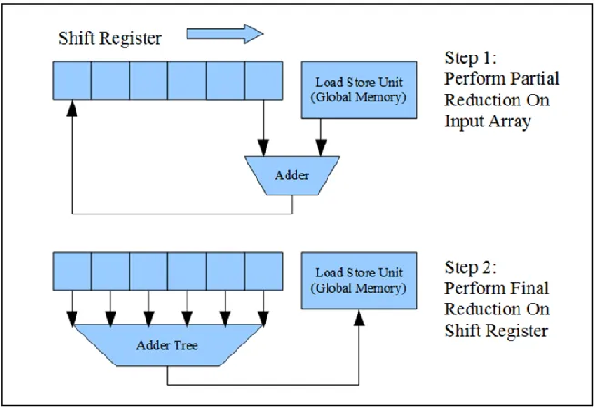
Altera SDK for OpenCL provides shift register inference feature that could relax some of
the data dependencies. The shift register inference is especially useful in applications
such as performing reduction operation on an array, or performing convolutions. In those
applications variables need to be constantly updated or read by different for loop
iterations. To utilize shift register inference in reduction sum for example, a shift register
array needs to be declared to hold the intermediate results from different iterations.
During each iteration of the loop, shift register shifts right, summation is performed on
the last element and the result is stored in the last element of the shift register. After all
the input data are used, a final reduction operation is performed on the shift register to get
26
Figure 9. AOCL Shift Register Inference
In many applications task parallelism may not be effective in realizing the full
potential of FPGA. In that case the multi-threaded NDRange kernels that are often seen
in CPU and GPU OpenCL programs are used. Similar to OpenCL implementation for
general purpose processors, in AOCL kernels vectorization could be applied to increase
throughput. The simplest way to vectorize is to utilize OpenCL vector data types such as
float4 or int8, although Altera OpenCL also supports SIMD style vectorization and
replication of Compute Units. Setting the attribute for number of SIMD work-items for a
kernel will allow AOC to replicate its datapath, and the resultant kernel will be able to
process multiple work-items in parallel. On the other hand, modifying the number of
Compute Units will allow the kernel to execute multiple work-groups concurrently.
Increasing the number of SIMD work-items is usually more efficient than increasing the
number of Compute Units, because SIMD vectorization generates less load store units for
27
To take the advantage of the flexibility of FPGA architecture, AOCL supports
compiler flag enabled floating point optimizations. In HDL design of floating point units,
normalization and rounding usually takes a lot of FPGA area. When multiple floating
point operations are performed in succession, --fpc compiler flag could be enabled to
allow AOC to eliminate the normalization and rounding in between the floating point
units, thus saving FPGA space and reduce latency. AOC could also reorder the floating
point operations to balance the operations and reduce number of stages in the pipeline
when --fp-relaxed flag is enabled.
AOCL also added a unique feature called channel extensions, which allows the
direct data transfer between different kernel without use of global memory or host
program. The channels are implemented using first in first out (FIFO) buffers inside
FPGA chip. Thus low latency high bandwidth memory transfer could be achieved
through use of channel. Due to the fact that Stratix V FPGAs has rather limited global
memory bandwidth comparing to GPUs, the use of channel extension could be essential
for AOCL applications that require large amount of global memory data transfer to
achieving high performance. However, kernel with channels could not utilize SIMD or
multi-Compute Unit vectorization. This tradeoff needs to be considered when developing
kernels using AOCL.
2.5 Detailed Analysis of AOCL
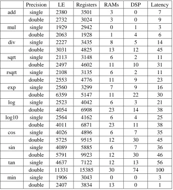
2.5.1 Cost of Floating Point and Integer Operations
In order to study the latency and hardware utilization for different types of
28
and the testing results was generated as shown in Table 1 and 2. The resource utilizations
of various types of operations are obtained by compiling identical NDRange vector
operation kernels and reading the resultant .area resource estimate file. The logic element
(LE), Register (Reg), Block RAM, and DSP counts are calculated by subtracting resource
utilized by load store unit (LSU) from the total kernel estimated utilization. Whereas the
latency is estimated by compiling task based kernels designed to repeatedly perform
operations in a data dependent loop, and reading the optimization report returned by the
compiler.
Table 1. Cost of Floating Point Operations in AOCL
Precision LE Registers RAMs DSP Latency
add single 2380 3501 3 0 7
double 2732 3024 3 0 9
mul single 1929 2942 0 1 3
double 2063 1928 1 4 6
div single 2227 3435 8 5 14
double 3031 4825 13 12 45
sqrt single 2113 3148 6 2 11
double 2497 4602 11 10 31
rsqrt single 2108 3135 6 2 11
double 2553 4776 11 9 23
exp single 2560 3299 7 9 16
double 6359 5147 11 22 30
log single 2523 4042 6 3 21
double 4054 6908 23 14 38
log10 single 2564 4162 6 4 25
double 4011 6871 23 11 38
cos single 4026 4896 6 7 35
double 5725 9515 12 30 45
sin single 4089 5885 6 7 36
double 5791 9923 12 30 46
tan single 4637 7122 12 13 56
double 11331 15385 30 74 100
min single 1906 3043 0 0 3
29
Table 2. Cost of Fixed Point Operations in AOCL
Precision LE Registers RAMs DSP Latency
add char 1751 2533 0 0 1
short 1779 2548 0 0 1
int 1835 2587 0 0 1
div char 2884 4541 18 4 32
short 2900 4548 18 4 32
int 2932 4571 18 4 32
min char 1751 2533 0 0 1
short 1772 2616 0 0 1
int 1803 2652 0 0 1
mul char 1749 2605 0 1 2
short 1773 2628 0 1 2
int 1822 2715 0 2 3
Note that the latency is measured in clock cycles. From the tables we can see that double
precision floating point operations cost a lot more than single precision operations both in
terms of FPGA area used and latency. Operations such as finding minimum and
multiplication are the least costly, whereas division, square root, logarithm, and
trigonometry operations cost the most FPGA area and time. Note that Stratix V A7
FPGA used in this research only has a total of 256 DSP units. High cost functions such as
double precision tangent should be avoided if possible.
2.5.2 Kernel Launch and Transfer Overhead
Other performance evaluations done on AOCL are summarized below. One of the
performance metrics that we are interested in is the speed of data transfer between kernel
and host. According to [27] the bandwidth of host to device data transfer for the GPU is
about 2.82 GB/s, with latency of 50~60 us whereas the bandwidth of device to host data
transfer is about 3.29 GB/s with latency of 140~150 us. The AOCL memory diagnostic
30
from device for Terasic DE5-net accelerator. The Nallatech 385 accelerator has slightly
higher global memory throughput of 2.46 GB/s host to device and 2.95 GB/s device to
host. There is no easy way to determine the latency, but FPGA should have comparable
latency to GPU. The throughput for data transfer between kernel and host is far lower
than the 25.6GB/s peak bandwidth of global memory, which means communication to
host should be minimized. The peak bandwidth of private and local memory is dependent
the kernel because FPGA does not have a fixed architecture, thus could not be accurately
determined.
Another important performance metric is the overhead of launching a kernel. The
test methodology used is to launch an empty kernel repeatedly, both with and without
synchronization between each kernel launch. For time keeping, the submitted and
execution time returned from OpenCL build-in profiler function as well as the wall clock
time recorded by the OS timer are both recorded and compared. The result is that when
launching a single kernel, the queued to submitted time is 0.004 ms and submit to start
time is 0.016 ms. When launching the kernel repeatedly for a large number of times and
synchronize after every kernel launch, although submit to start time increases linearly
with respect to the number kernel launches, the wall clock time increases very rapidly (20
s for 10000 launches). When the clFinish function used to synchronize the kernel
launches is replaced with clFlush function that issues the kernel launch command without
waiting for operations to finish, the wall clock time is reduced to more acceptable 7 s for
10000 launches. When launching kernels without synchronization, the wall clock time
31
launch should be minimized to reduce overhead. At the same time it is often more
effective to use multiple workgroups kernel, than launch the kernel multiple times.
2.5.1 Effective Reduction
Reduction is one of the common patterns in parallel computing. It reduces an
array of data into a single output by repeatedly performing some type of reduction
operation. The reduction operation could be summation, product, or finding min/max.
The computational complexity of reduction is O (N), and since the number of operations
performed is equal to data size, reduction speed is bounded by global memory bandwidth.
For the accelerator that we have, the theoretical maximum single precision reduction
throughput is 6.4 GFLOPS. This is calculated from dividing 25.6 GB/s maximum
bandwidth by 4 byte per floating point value.
Altera recommends [28] performing reduction by using a single threaded kernel.
If a simple for loop is used to perform reduction, one iteration could only start after the
pervious iteration is completed. This is due to memory dependency on the partial result.
Since most operations take multiple clock cycles to complete, the performance will suffer
greatly as a result. At the same time loop unrolling could not be effectively applied to
increase the throughput. Without any optimization the loop version of reduction could
only achieve 0.035 GFLOPS throughput. To relax data dependencies, Altera
recommends replicating the partial sum storage register and implementing a shift register
to perform reduction. The parallelism is extracted by unrolling the loop to ensure multiple
reduction operations are done concurrently. Test shows that the throughput for this
un-32
optimized version, but still far from maximum throughput because it could not saturate
the global memory bandwidth of the FPGA.
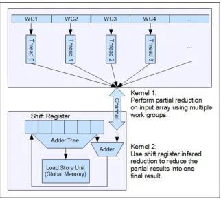
Inspired by multi-thread solutions introduced by GPU vendors, various test
kernels were developed. The most efficient way to implement reduction is determined to
be using two kernels. In this method, the input data is partitioned into equally sized
blocks. An NDRange kernel first processes different blocks of the input array
simultaneously, then a second task kernel reduces the partial sum into a single value. The
second kernel is implemented the same way as Altera programming guide recommended,
but it will only perform a small portion of computation, whereas the vast majority of the
calculation is done by the first kernel. The two kernels are connected via channel to avoid
wasting global memory bandwidth. There are a few different ways the first kernel could
be implemented. The simplest way is by launching single work-item work-groups, each
work-item loops through one block of data and computes the partial sum. The loop could
be unrolled to increase throughput effectively. Since in NDRange kernel each pipeline
stage processes a different work-item instead of loop iteration, there is no data
dependency. The block diagram for this implementation is shown in Figure 10. The
optimal block size is dependent on input data size. The first NDRange kernel is only
efficient when data block is large enough to fill the pipeline, and the number of blocks
has to be small enough so that the less efficient task kernel does not take too long to
finish. For example, when performing sum reduction on 1GB data, the best block size is
32, which will produce 3.70GFLOPS throughput on Terasic DE5-net accelerator or
4.03GFLOPS throughput on Nallatech 385 accelerator. Those throughput numbers
33
which is satisfactory. The full source code for reduction kernel with addition operations
can be found in Appendix A.
In an attempt to improve memory access efficiency, another NDRange kernel
with multi-threaded groups was also developed. The kernels use multiple
work-items to reduce each block instead of single work-item. In order to ensure coalesce
memory access, consecutive input data is accessed by successive work-items. This
version of the parallel reduction did not outperform the simple implementation during test
and thus was discarded.
Figure 10. Optimized Two Kernel Reduction Block Diagram
Very little hardware was needed to generate enough performance to saturate the
relatively small FPGA global memory bandwidth. On DE2-net accelerator the fully
34
blocks, and runs at 236.85 MHz. On Nallatech 385 accelerator, similar amount of FPGA
resources were used, but the kernel is clocked at slightly higher 260.89 MHz. The
knowledge gained from developing the reduction kernel here was also used in designing
the k-means kernels in chapter 4.
2.6 Brief Summary of Algorithms used in Acceleration
The algorithms explored in this thesis include k-means clustering, k-nearest
neighbor, N-body algorithms, and LU matrix decomposition. This thesis devotes one
chapter to each of the listed algorithms.
K-means clustering algorithm is one of the most popular data mining algorithms
used in image processing and machine learning. It is very time-consuming for large data
and cluster sizes. In this research, an optimized implementation of k-means clustering
algorithm on FPGA was developed using Altera SDK for OpenCL. Performance and
power consumption of FPGA implementation are measured and compared against CPU
and GPU implementations.
K-nearest neighbor (kNN) is another popular machine learning algorithm that
classifies the query points by compares their distance between training points. The
classification of a query point is determined by the classes of k training points closest to
the query point. It is commonly used in machine learning and data mining applications.
This research focused on implementation of brute force k-nearest neighbor algorithm
using AOCL and the results are compared with best published works.
N-body simulation simulates dynamic interaction of particles. It is often used in
35
this research is pair-wise method with time complexity of O (N2) for each iteration. The
results are compared with optimized CPU and GPU implementation.
LU decomposition factorizes a matrix into the product of a lower triangular
matrix and an upper triangular matrix, hence the name. This method is useful in solving
linear systems of equations and finding inverse, and has been implemented in many
computing libraries such as LAPACK, cuBLAS, MKL etc. This research tries to
determine if the blocked LU decomposition algorithm could be implemented on FPGA
using AOCL to achieve performance comparable with existing optimized CPU and GPU
implementations provided in numerical libraries.
For consistency, all OpenCL kernels developed and tested on FPGA in the
![Figure 1. Intel Nehalem Architecture [6]](https://thumb-us.123doks.com/thumbv2/123dok_us/1390300.1171729/24.612.166.481.71.387/figure-intel-nehalem-architecture.webp)
![Figure 2. NVIDIA Kepler Architecture [10]](https://thumb-us.123doks.com/thumbv2/123dok_us/1390300.1171729/27.612.161.486.219.566/figure-nvidia-kepler-architecture.webp)
![Figure 4. Stratix V FPGA Architecture [13]](https://thumb-us.123doks.com/thumbv2/123dok_us/1390300.1171729/31.612.106.544.221.477/figure-stratix-v-fpga-architecture.webp)
![Figure 5. Stratix V FPGA ALM Layout [14]](https://thumb-us.123doks.com/thumbv2/123dok_us/1390300.1171729/32.612.108.542.194.464/figure-stratix-v-fpga-alm-layout.webp)
![Figure 6. DE5-Net Accelerator Board Layout [18]](https://thumb-us.123doks.com/thumbv2/123dok_us/1390300.1171729/34.612.107.543.71.282/figure-de-net-accelerator-board-layout.webp)
![Figure 7. Altera OpenCL to FPGA Framework [23]](https://thumb-us.123doks.com/thumbv2/123dok_us/1390300.1171729/37.612.135.515.273.538/figure-altera-opencl-fpga-framework.webp)
![Figure 8. Example Hardware Architecture Synthesized by AOCL [25]](https://thumb-us.123doks.com/thumbv2/123dok_us/1390300.1171729/38.612.123.524.162.383/figure-example-hardware-architecture-synthesized-aocl.webp)