ABSTRACT
CHEN, YIFENG. Electron, Spin and Heat Transport in Nanoscale Systems and Devices.
(Under the direction of Marco Buongiorno Nardelli.)
This thesis focuses on the studies of electron, spin and heat transport through nanoscale
systems and devices from computational methods. Both tight binding and first principle den-sity functional theory (DFT) methods are employed. The coherent goal of this thesis is to
explore advanced applications of nanoscale structures such as graphenic systems and
magnet-ically bi–stable molecular complex systems. Fundamental properties of these systems need to be understood. Modifications and functionalizations are crucial for realistic device applications.
For graphenic systems, we studied thermal transport and thermoelectric properties from tight binding methods. Our main focus is on graphene nanoribbon (GNR) systems and derived
structures. Interface effects between ribbons of different widths are taken into account by
us-ing a general conductor case carrier transport Green’s function formalism within the Landauer regime. We found optimal thermoelectric properties of GNR superlattices and chevron-type
GNRs. The key is to substantially reduce thermal conductance of the system while at the same
time do not quench electronic conductance too much.
For magnetically bistable functional molecular complex systems, including Cobalt-based
va-lence tautomeric (VT) complexes and Fe(II) spin crossover (SCO) complexes, we are focusing on investigating their electronic structure, electron and spin transport properties from several
different configurations of these complexes. Here we employed first principle DFT methods for electronic structure calculations as implemented in the Quantum-ESPRESSO method. First
principle transport properties are calculated using the Wannier function transport method
WanT. Electronic structures of these molecular complexes upon magnetic transitions are all correctly predicted by our first principle DFT methods from local spin density approximations
(LSDA) and constrained magnetization methods. In Cobalt-based VT polymeric systems, we
found interesting current switching behaviors and exotic spin valve effects. In Fe(II) SCO molecular wire-like stacking structures, current switching behaviors of the LS and HS states are
also obvious. Our computational studies of Fe(II) SCO molecular dimer structures, together
with experimental observations of the bilayer coverage ultrathin films on Au(111) substrate, revealed novel magnetic behaviors of these systems under unconventional situations. Single
molecule physisorption of the Fe(II) SCO molecule on Au(111) is also briefly investigated. The
Finally, chemisorption of one kind of Cobalt-based VT systems on Au(111) substrate is in-vestigated. This is a first step toward realistic device utilizations of these functional molecular
complexes in real-life applications. A Au(111) cluster nanolead was subsequently constructed
to bridge with the molecule to form gold nanolead – molecule – gold nanolead device structures.
Our consistent efforts here throughout this thesis are converging towards scientific
investi-gations and realistic applications of these nanoscale systems and devices. A focus was put on transport properties. Our studies revealed very interesting behaviors of these systems and
sug-gested many different possibilities for their integration into potential important applications.
c
Copyright 2013 by Yifeng Chen
Electron, Spin and Heat Transport in Nanoscale Systems and Devices
by Yifeng Chen
A dissertation submitted to the Graduate Faculty of North Carolina State University
in partial fulfillment of the requirements for the Degree of
Doctor of Philosophy
Physics
Raleigh, North Carolina
2013
APPROVED BY:
Daniel Dougherty David A. Shultz
Wenchang Lu Marco Buongiorno Nardelli
DEDICATION
BIOGRAPHY
• Graduate Student Sep. 2008 - now
Graduate Research Assistant, Advisor: Prof. Marco Buongiorno Nardelli Research Topic: Quantum transport in nanoscale structures
Department of Physics, North Carolina State University, Raleigh, North Carolina, U.S.A.
• Bachelor’s Degree in Physics, Sep. 2004 - July 2008
Undergraduate Thesis Advisor: Prof. Hao Chen
Thesis Topic: Theoretical investigations of coherent transport properties of electrons in a
double-quantum-dot (DQD) system Fudan University, Shanghai, P.R. China
• High School Diploma Sep. 2001 - June 2004
ACKNOWLEDGEMENTS
I would like to thank my PhD advisor, Dr. Marco Buongiorno Nardelli, for his support of my
PhD work. He introduced me to this research field and provided me with numerous invaluable guidance and insights along the way towards this thesis.
I would like to thank Dr. Arrigo Calzolari for his patience and numerous technical helps to me in getting things running.
I would also like to thank my dissertation committee: Dr. Daniel Dougherty, Dr. David A. Schultz and Dr. Wenchang Lu, for their efforts with me to finally work out this thesis.
I would like to thank the molecular spintronics center collaborations for providing me a broad scope of view of what I was doing, otherwise unavailable by just working in my own field.
I would like to thank people from the Department of Physics for all the helps in facilitating my PhD studies in NC State. They include: graduate program director Dr. Harald Ade, graduate
program secretaries and department secretaries Megan Freeman, Rebecca Savage, and Inga
Wilson. And ChiPS center secretaries Cecillia Upchurch and Jennifer Outlaw.
During the work of this thesis, I have received numerous helps from a number of parallel super-computing facilities and the corresponding maintenance crew of those facilities. They include:
HPC Supercomputer at NC State University, Medusa at ChiPS, Jaguar Supercomputer (Now
upgraded to Titan) at Oak Ridge National Laboratory, Talon Supercomputer at UNT, and TACC Supercomputer at UT-Austin. These invaluable resources and helps made possible
al-most all the computations I have done for this thesis. Thanks very much!
I wanted to thank many people who I have interacted with in the ChiPS center for high
perfor-mance simulations. They include: Chengbo Han, Bikan Tan, Shi Guo, Shu Xu, Jeffery Mullen,
Thushari Jayasekara, Byoung-Don Kong, Xiaodong Li, Sujata Paul, Frisco Rose, Jie Jiang, Rui Dong, Rui Mao, Yan Li and Wanderla Scopel.
TABLE OF CONTENTS
List of Tables . . . vii
List of Figures . . . .viii
Chapter 1 Introduction . . . 1
1.1 Nanoscience and Nanotechnology . . . 1
1.2 Quantum Transport . . . 2
1.3 Organization of the Thesis . . . 4
Chapter 2 Graphene Derived Nanostructures . . . 6
2.1 Introduction and Motivations . . . 6
2.2 Methodologies of Green’s Function Transport within Linear Response Regime . . 9
2.2.1 The Landauer Formula and Green’s Function Formalism . . . 9
2.2.2 Tight-binding Models . . . 12
2.2.3 Various Integration Formulae . . . 14
2.3 Results and Discussions . . . 15
2.3.1 Phonon Dispersions and Phonon Transmissions of Pristine GNRs . . . 15
2.3.2 Thermoelectrics of Pristine AGNRs . . . 17
2.3.3 Thermal Transport and Thermoelectrics of GNR Junctions . . . 18
2.3.4 Thermoelectrics of GNR Superlattices . . . 24
Chapter 3 First Principle Methods and Localized Wavefunction Basis . . . 27
3.1 Density Functional Theory Methods . . . 28
3.2 Plane Wave Basis and the Quantum-ESPRESSO Implementation . . . 32
3.3 Localized Wavefunction Basis . . . 33
3.3.1 Wannier Basis . . . 34
3.3.2 Atomic Basis . . . 35
3.4 Other First Principle Methods . . . 36
Chapter 4 Cobalt-based Semiquinone Catecholate Valence Tautomeric Com-plexes . . . 38
4.1 Introduction . . . 38
4.2 Gas Phase Monomers . . . 42
4.2.1 Coordination VT Monomers . . . 42
4.2.2 Conjugation VT Monomers . . . 46
4.3 Valence Tautomeric Polymers . . . 50
4.3.1 Coordination VT Polymers . . . 50
4.3.2 Conjugation VT Polymers . . . 54
Chapter 5 Fe(II) Spin Crossover Complexes . . . 58
5.1 Introduction . . . 58
5.2 Isolated Molecules: Molecular and Electronic Structures . . . 59
5.2.1 Single Molecules . . . 59
5.2.2 Simple Molecular Wire-like Stackings . . . 63
5.3 Molecular Dimer Structures . . . 65
5.3.1 Molecular Dimers . . . 65
5.3.2 Molecular Wire-likeπ-Stackings . . . 69
5.4 Physisorption of Single Molecule on Au(111) Substrate . . . 72
5.5 Conclusions . . . 75
Chapter 6 Cobalt-based Coordination VT Molecule on Au(111) and Device Structures . . . 76
6.1 Chemisorption of Cobalt-based Coordination VT Molecule on Au(111) . . . 76
6.2 Cobalt-based Coordination VT Molecule Sandwitched between Two Au(111) Nanoleads . . . 80
6.3 Conclusions . . . 83
Chapter 7 Summary and Outlook . . . 85
7.1 Summary . . . 85
7.2 Future Perspectives . . . 87
References . . . 89
Appendices . . . .102
Appendix A Technical Details of First Principle DFT Implementations . . . 103
A.1 Pseudopotentials: Norm Conserving and Ultrasoft . . . 103
A.2 LDA, LSDA and GGA . . . 105
A.3 Types of Exchange-Correlation Functionals . . . 106
A.4 Hellman-Feynman Theorem, Force and Stress . . . 107
A.5 Van der Waals Forces . . . 108
A.6 Other Deficiencies of Conventional DFT Formalism . . . 108
A.7 Tersoff-Hamann Model for STM Image Simulations . . . 109
LIST OF TABLES
Table 2.1 Three highest ZT peak values and their corresponding chemical potential
for various AGNR superlattices. . . 22
Table 2.2 Three highest ZT peak values and their corresponding chemical potential
for various ZGNR superlattices. . . 23
Table 4.1 Comparison of Co-L bondlengths (˚A) and several properties of the
low-spin CoIII versus high-spin CoII coordination VT molecule:
COORDINA-TION ISOLATED MOLECULE. HS induced by constrained magnetization. 44
Table 4.2 Comparison of Co-L bondlengths (˚A) of the low-spin CoIII versus
high-spin CoII: CONJUGATION ISOLATED MOLECULE. . . 47
Table 4.3 Comparison of Co-L bondlengths (˚A) and several relevant parameters
of the low-spin CoIII versus high-spin CoII configuration from relaxed
two-monomer unit cell Cobalt-based VT coordination polymeric systems (ferromagnetic configuration). . . 51
Table 4.4 Comparison of Co-X bondlengths (˚A) and several relevant parameters
of the low-spin CoIII versus high-spin CoII configuration from relaxed
two-monomer unit cell Cobalt-based conjugation VT polymeric systems (ferromagnetic configuration). . . 54
Table 5.1 Comparison of Fe-L bondlengths (˚A) and several properties of the
low-spin Fe(II) SCO compound versus high-low-spin: ISOLATED MOLECULE. HS induced by constrained magnetization along the vertical direction. . . . 60
Table 6.1 Comparison of properties of chemisorbed structures of the low-spin CoIII
and high-spin CoII coordination VT molecule on Au(111) at both bridge
LIST OF FIGURES
Figure 1.1 Length scales from 1×10⁻¹¹ m to 10 m. . . 3
Figure 2.1 (a) The real space 2D hexagonal lattice of graphene, shaded region is one
unit cell of graphene. (b) The reciprocal space IBZ of graphene is shaded.
High symmetry points Γ, M, K, K0 are respectively marked. . . 7
Figure 2.2 Molecular structures for (a) 4-ZGNR and (b) 6-AGNR. Shaded regions
are one of their unit cells, respectively. . . 8
Figure 2.3 Principal layers and transfer matrices for a bulk-like conductance structure 9
Figure 2.4 Principal layers and interacting Hamiltonians for a general lead-conductor-lead case structure. . . 11
Figure 2.5 Concentric circles showing up to 4th nearest neighbors for both type A
(empty circles) and type B (filled circles) carbon atoms. From Ref.[1]. . . 12
Figure 2.6 4-NNFC models to construct the force constant matrices, shown here are
for 1st nearest neighbors. From Ref.[1]. . . 12
Figure 2.7 Phonon dispersion of graphene from the force constant parameters we
have adopted. . . 15
Figure 2.8 (a) Phonon dispersion and phononic transmission for a pristine 6-AGNR
from tight binding 4-NNFC model. (b) Phonon dispersion and phononic transmission for a pristine 4-ZGNR from tight binding 4-NNFC model (Black solid lines) and from first principle density functional perturbation theory (DFPT) [2] (Red dashed line)(Note that there are spurious modes in the first principle dispersion which are from carbon-hydrogen vibrations because in first principle calculations we have saturated the ZGNR edges with hydrogen atoms). . . 16
Figure 2.9 Normalized ZT factor, total thermal conductance, electronic conductance
and thermopower of a pristine 15-AGNR. . . 17 Figure 2.10 Tight binding energy gap (black, circles) and peak ZT (red, squares) as a
function of width in ideal AGNRs with indices N = 3, 4, 6, 7, 9, 10, 12, 13, 15, 16, 18, 19. ZT factors values are all evaluated at room temperature (T = 300 K). . . 18 Figure 2.11 Molecular structures of single interface semi-infinite 4-2 ZGNR junction
(a) and 6-3 AGNR junction (b). . . 19 Figure 2.12 Phonon transmissions of single interface 4-2 ZGNR semi-infinite junction
(a) and 6-3 AGNR semi-infinite junction (b). . . 19 Figure 2.13 Upper panel: thermal conductance of 12 AGNR (red dotted), 6-AGNR
Figure 2.14 Thermoelectric figure of merit ZT values of 4-2 ZGNR semi-infinite junc-tions with 5 (solid), 7 (dashed), 9 (dotted) and 11 (dasheddotted) inter-faces in the conductor region. The zero in the chemical potential is chosen as the center of the energy gap. . . 21 Figure 2.15 Highest ZT peaks for AGNR and ZGNR superlattice junctions: (left
panel) AGNR superlattice junctions with the narrow end fixed at 3-AGNR, 6-AGNR and 9-3-AGNR, respectively; (right panel) ZGNR super-lattice junctions with narrow end fixed at 2-ZGNR, 4-ZGNR and 8-ZGNR, respectively. . . 24 Figure 2.16 Continuous line shows the thermal conductance of a chevron-type GNR
(inset) and the dashed line shows the thermal conductance of the same-width straight 9-AGNR. . . 25 Figure 2.17 Electronic transmission (black, dashed) and thermoelectric figure of merit
ZT (red, solid) for a chevron-type GNR. The zero in the chemical poten-tial is chosen as the center of the energy gap. . . 26
Figure 3.1 The Kohn-Sham ansatz reformulation of the many body problem. . . 29
Figure 3.2 Flow chart for solving the Kohn-Sham equations self-consistently. In
general, two such loops are iterated simultaneously for spin up and spin down components, respectively. From Ref. [3] Section 9.1. . . 30
Figure 4.1 Structures of the Cobalt-based VT coordination complex, at both low
spin ls−CoIII(Cat)(SQ)(4-CNpy)
2 (left) and high spin hs−CoII(SQ)2
(4-CNpy)2 (right) states. SQ = dimethyl-o-semiquinone; Cat =
3,5-dimethyl-catechol; 4-CNpy = 4-cyanopyridine. Elements between square parentheses identify the repeated monomers in the corresponding poly-meric structures. . . 39
Figure 4.2 Molecular structure of the Co-based VT coordination polymer from two
different points of views. The polymerization direction is along the verti-cal z axis. . . 40
Figure 4.3 Structures of the Cobalt-based VT conjugation complex, at both low
spin ls−CoIII(Cat)(SQ) L (left) and high spin hs−CoII(SQ)
2 L (right) states, where L is a π-electron conjugation backbone, with a bi-pyridine (bpy) ligand in it to bond with the Cobalt atom. . . 40
Figure 4.4 (a) Molecular structures of the conjugation VT molecule in the LS state;
(b) The corresponding polymeric form with two monomers per unit cell. . 41 Figure 4.5 Charge density distribution (|ψ|2) of characteristic t
2g, eg and e∗g orbital
levels for the Cobalt-based coordination VT monomers. Insert: Spin
component occupations for the LS and HS states, respectively. . . 43
Figure 4.6 DOS (Black line) and LDOS (Red line) on Cobalt atoms of the
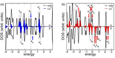
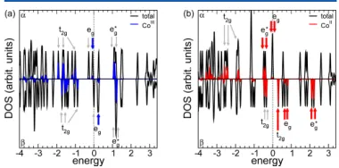
Figure 4.7 DOS (Black line) and LDOS (Red line) on Cobalt atoms of the coor-dination VT isolated molecule in the high spin state from constrained magnetization method. Black arrows are pointing to occupied orbitals, while red ones are unoccupied orbitals. The upper panel is for spin up, the down panel is for spin down. . . 45
Figure 4.8 DOS (Black line) and LDOS (Red line) on Cobalt atoms of the
coordina-tion VT isolated molecule in the high spin state from GGA+U method. The upper panel is for spin up, the down panel is for spin down. . . 46 Figure 4.9 Charge density distribution (|ψ|2) of characteristic t
2g, eg and e∗g orbital levels for the Cobalt-based conjugation VT monomers. Insert: Spin com-ponent occupations for the LS and HS states, respectively. . . 47 Figure 4.10 DOS (Black line) and LDOS (Red line) on Cobalt atoms of the
con-jugation VT molecule in the low spin state. Black labels are pointing to occupied orbitals, while red ones are unoccupied orbitals. The upper panel is for spin up, the down panel is for spin down. . . 48 Figure 4.11 DOS (Black line) and LDOS (Red line) on Cobalt atoms of the
conjuga-tion VT molecule in high spin state induced by the constrained magneti-zation method. Black labels are pointing to occupied orbitals, while red ones are unoccupied orbitals. The upper panel is for spin up, the down panel is for spin down. . . 49 Figure 4.12 DOS (Black line) and LDOS (Red line) on Cobalt atoms of the
conju-gation VT molecule in high spin state induced by the GGA+U method. The upper panel is for spin up, the down panel is for spin down. . . 49 Figure 4.13 The total energy of fully relaxed bipyridine bridged coordination polymer
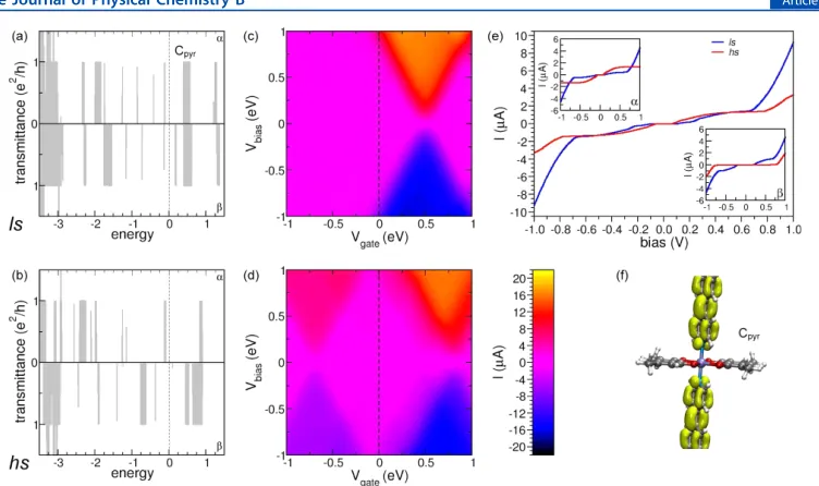
at different vertical cell dimension value. We have chosen celldm(3) = 0.806 · celldm(1) as our final optimal vertical cell dimension for the HS state. . . 51 Figure 4.14 (a) Spin resolved transmission spectra (Tel) for the coordination polymer
in the LS configuration, top panel for spin up (αspin channel in chemistry
literature) and bottom panel for spin down component (β spin channel in
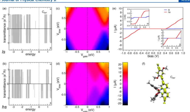
chemistry literature); (b) same as part (a) but for the HS configuration; (c) current as a function of both bias and gate voltage for LS; (d) same as part (c) but for HS; (e) current vs bias voltage at Vg = 0 eV, insets: spin resolved currents for the spin up and spin down components; (f) transport eigenchannel for one representative state labeled Cpyr in part (a). . . 52 Figure 4.15 (a) Spin resolved transmission spectra (Tel) for the conjugation polymer
Figure 5.1 Chemical formula (a) and molecular structure (b) of the isolated molecule in the relaxed low spin state. The vertical direction is along the z axis, while the bipyridine ligand is perpendicular to the vertical direction. Shown here is the δ-enatiomer of the molecule. . . 59 Figure 5.2 Charge density distribution (|ψ|2) of characteristic Fe d-shell t
2g and eg orbital levels for the Fe(II) spin crossover complexes in the isolated single molecular form. Insert: Spin component occupations for the LS and HS states, respectively. . . 61
Figure 5.3 Total DOS (Black) and Fe LDOS (Red) for the relaxed isolated Fe(II)
SCO single molecule in the low spin configuration. The upper panel is for spin up states, while the down panel is for spin down . . . 62
Figure 5.4 Total DOS (Black) and Fe LDOS (Red) for the relaxed isolated Fe(II)
SCO single molecule in the high spin configuration. The upper panel is
for spin up component, while the down panel is for spin down. . . 62
Figure 5.5 Vertical cell dimension optimization for the low spin (left) and high spin (right) states in the simple molecular wire-like stacking configurations with London dispersion forces taken into account. . . 63
Figure 5.6 Transport results for the simple wire-like stackings of the Fe(II) SCO
compound in both the low spin (blue dashed) and the high spin (red solid) states. . . 64
Figure 5.7 (a) High resolution STM image (12 nm×12 nm, V=-1 V, I=1 nA) of the
Fe(II) SCO molecular bilayer film on Au(111) substrate with molecular tiling overlaid Insert is a zoom in view of a depression.(b) Single point dI/dV scanning tunneling spectroscopy (STS) curves measured above ei-ther 3-lobed features (red dashed) or apparent depressions with isolated
lobes (blue solid) at 131 K. From Alex Pronschinske. . . 66
Figure 5.8 (a) Geometry of the DFT calculation ofπ-stacked Fe-bpy molecules in the
proposed bilayer geometry (Au substrate position is illustrated schemat-ically, not calculated); (b) Spin-averaged theoretical DOS for high-spin (HS, blue solid) and low-spin (LS, red dashed) configurations. Vertical lines indicate the electron energy spectrum of the system while the DOS curves are broadened with a Gaussian spreading of 0.02 Ry to mimic the experimental resolution. The zero of energy is taken as the mid-point of the HOMO- LUMO gap of the HS state, which agrees qualitatively with the experimental reference. (c),(d) Simulated STM images of low-spin and high-spin states with molecular dimer structure overlaid. . . 67
Figure 5.9 Molecular wire-like π-stacking structures of the Fe(II) SCO compound
for both the low spin (left) and the high spin (right) states. . . 69
Figure 5.10 Transport results for the π-stackings of the Fe(II) SCO compound in
both the low spin (red dashed) and the high spin (black solid) states. . . 70
Figure 5.11 Experimentally measured I-V curves of the Fe(II) SCO complex in dis-ordered films form in both the low spin (red) and the high spin (green)
Figure 5.12 Charge difference of single Fe(II) SCO molecule physisorbed on Au(111) substrate before and after the adsorption in two conformations (see text) from the constrained magnetization low spin state calculation. Red means charge lost after the physisorption, blue means charge gained after the physisorption. . . 73
Figure 6.1 Three layer FCC close-packing structure of the Au(111) surface. Several
adsorption sites on the top C layer are also shown. Bridge sites are
between pairs offcc hollow sites and hcp hollow sites. . . 77
Figure 6.2 Low spin chemisorbed structures of the coordination VT molecule on
Au(111) surface for (a) the bridge site , and (b)fcchollow site , respectively. 77
Figure 6.3 Low spin total DOS, Cobalt LDOS, SQ Cat summed PDOS of the
coor-dination VT molecule on Au(111) surface for (a) the bridge site , and (b)
fcc hollow site , respectively. . . 79
Figure 6.4 High spin total DOS, Cobalt LDOS, SQ Cat summed PDOS of the
co-ordination VT molecule on Au(111) surface for (a) the bridge site , and (b) fcc hollow site , respectively. . . 81
Figure 6.5 (a) CAB three layer repeating Au(111) cluster nanolead structure. (b)
Total DOS of the structure shown in (a). Fermi level is aligned at zero. (c) Electronic transmission through the horizontal periodic direction on the energetics spectrum. Fermi level is aligned at zero. (d) Integrated I-V curve. . . 82
Figure 6.6 A gold nanolead – molecule – gold nanolead device structure. . . 83
Figure A.1 (a) Norm conserving pseudopotential compared with all-electron
pottial for Oxygen 2s orbital. From http://th.physik.uni-frankfurt.de/ en-gel/ncpp.html (b) Ultrasoft pseudopotential, norm conserving pseudopo-tential compared with all-electron popseudopo-tential for Oxygen 2p orbital. From
David Vanderbilt, Phys. Rev. B 41, 78927895 (1990). . . 104
Chapter 1
Introduction
‘‘To see a World in a Grain of Sand And a Heaven in a Wild Flower, Hold Infinity in the palm of your hand And Eternity in an hour’’ -- William Blake
1.1
Nanoscience and Nanotechnology
The field of nanoscience and naontechnology emerged from several different perspectives, all
converged now in efforts to directly manipulate individual atoms or molecules, and make use out
of them, as par Richard P. Feynman’s famous lecture in 1959 titled There is Plenty of Room
at the Bottom. Experimentally, the invention of scanning probe microscopies such as Scan-ning Tunneling Microscopy (STM) and Atomic Force Microscopy (AFM) in the 1980s made it possible for the mankind to directly visualize and manipulate atoms individually for the
first time. High resolution microscopies such as Transmission Electron Microscopy(TEM),
to-gether with novel precise device fabrication methods, such as Molecular Beam Epitaxy (MBE), nanolithography, etc., make nanoscale device manipulation and characterization a fruitful task
for both scientific researches and industrial applications. The discovery of fullerenes, carbon
nanotubes, nanowires, and recently graphene, all offered new possibilities into the investiga-tions and utilizainvestiga-tions of nanoscience and nanotechnology. From the molecular side, functional
groups synthesized systems and molecular self-assembled structures offer bases for
molecu-lar scale electronics, not to mention the potentially even more valuable direction of utilizing nanoscale biological systems for medical applications. The advent of microelectronics is also
pushing the limits of conventional semiconductor industry into nanoscale devices. For example,
following Moore’s law. The technological achievements feed back to the underlying science
and investigations, and advancements of the underlying science and investigations continued to bring about new technological breakthroughs, thus forming a positive circle of science and
technology developments. Finally, from the computational science perspective, the
develop-ment of new and accurate quantum mechanics and quantum chemistry methods, facilitated by the dramatical increase of computational power available to the research community, made it
possible to investigate crucial properties of nanoscale systems from computational simulations
or to design and validate new materials from modeling, which is much cheaper and easier to do than in real life laboratories. Thus, computational simulations provide an invaluable tool for
nanoscience and nanotechnology.
Broadly speaking, nanoscience and nanotechnology refers to all kinds of phenomena that
occur in systems with nanometer (1 nanometer = 1×10⁻⁹ meter, usually abbreviated as 1 nm)
dimensions. 1 nm is essentially the smallest size of all phenomena occurring in regular chemistry,
materials science, and biology. Figure 1.1 shows the length scales from the nano-world to everyday lives. Usually, the most interesting systems to nanoscience and nanotechnology fall
into the lengthscale between 1 nm to 100 nm.
Many books [4, 5, 6, 7, 8, 9] sprout out of this field and continues to appear [10, 11], and a series of peer reviewed scientific journals are dedicated completely to the field such
as Nanotechnology by the Institute of Physics (IOP), UK, Nature Nanotechnology by Nature
Publishing Group, Nano Letters, ACS Nano by the American Chemical Society (ACS), etc.
Other research articles on the field regularly appear in general physics or chemistry journals
and beyond. In essence, nanoscience and nanotechnology is a highly interdisciplinary field that involves all those subjects such as physics, chemistry, biology, materials science, engineering,
etc, and promising in various kinds of important and ground-breaking applications.
1.2
Quantum Transport
One of the most crucial properties in the nanoscale is the carrier transport phenomenon.
How-ever, at length scales this small, quantum mechanical effects inevitable come into play.
Quan-tum transport studies constitute an essential and intellectually challenging part of nanoscience [12, 13, 14, 15]. Historically, the field of quantum transport descends from the field of
meso-scopic physics emerged in the early 1980s. Mesomeso-scopic physics deals with materials of sizes
between the size of an atom (i.e., around 1 nm) and sizes of about micrometers, which are the lower limit of the macroscopic scale. The most important difference of mesoscopic physics from
macroscopic physics is that the significance of quantum mechanical physics in mesoscopic scale has been much too large to be ignored. While on the other hand, mesoscopic systems still have
methods is yet practically possible. The need for an accurate and insightful description of
transport phenomena in the nanoscale brought great advancements in the field of mesoscopic physics, and later in the field of quantum transport.
In mesoscopic systems, electronic wave coherence and interference phenomena manifests
themselves surprisingly even with a substantial presence of disorders. These disorders are called static disorders because they do not destroy phase coherence and do not introduce irreversibility.
The electron phase coherent length,Lφ, denotes the length an electron travels before its initial phase is destroyed. Depending on material, temperature and other external conditions, phase coherent length can go up to as large as a few micrometers. This introduces fertile grounds in
mesoscopic scales in which quantum coherence effects can be taken into play.
For systems with size comparable or smaller than the electron mean free path Lm, we enter the ballistic transport regime. In the ballistic regime, the electrons will travel through systems
without any scattering mechanisms. The restrictions for electronic transport in these systems
are only the intrinsic constraint of the number of modes available and the topological structures of the systems. Ballistic transport is inherently coherent, and allows us to investigate transport
problems starting from the Schr¨odinger equation. The most important development of coherent
quantum transport theory is the famous Landauer-B¨uttiker formalism, in which Landauer first
proposed in ballistic systems electronic conductance is proportional to the average transmission
probability of electrons through the system. Usually this concept need to be applied within
the phase coherence regime where the scattering S-matrix can be defined. But later B¨uttiker
generalized the concept into multiple probes (i.e. leads) systems and proposed to
phenomeno-logically including phase-breaking mechanisms as conceptual floating probes. The Landauer-B¨uttiker formalism received great success in quantum transport modeling. Our Green’s function
transport scheme presented in this thesis rests within the Landauer-B¨uttiker formalism.
1.3
Organization of the Thesis
The following parts of this thesis are organized as follows:
In Chapter 2, we present the methodologies and results of tight-binding model studies of
graphene derived nanostructures. Both electronic and thermal transport properties of these systems are investigated, and they are combined together to give the thermoelectric properties
of the respective systems.
In Chapter 3, we introduce the methodologies of first principle density functional theory (DFT) methods and localized wave function basis sets, which sets the foundation for the studies
of the next several chapters to come. The rest parts of this thesis are mainly concerned about molecular complex studies from first principle DFT methods and towards molecular spintronic
In Chapter 4, we present the studies of electronic structural and electronic transport
prop-erties of Cobalt-based semiquinone catecholate valence tautomeric systems. The electronic transport properties across single-stranded valence tautomeric (VT) polymers are especially
interesting to investigate and exploit.
In Chapter 5, we present the studies of a kind of Fe(II) spin crossover (SCO) complex sys-tems. We compare our computational DFT studies with experimental STM studies and found
interesting novel behaviors of this system in bilayer coverage on Au(111) substrate. Electronic
transport studies are carried out on molecular wire-like stacking geometries. Physisorption of single Fe(II) SCO molecule on Au(111) substrate is investigated.
In Chapter 6, we study chemisorption of coordination VT molecules on Au(111) substrate
bridged by the thiol group. Subsequently, we investigated electronic transport through a
Au(111) cluster nanolead, and a gold nanolead-molecule-gold nanolead device structure was
constructed based on the chemisorption geometry we have obtained.
Chapter 7 concludes all of the thesis and presents future perspectives from this thesis. Ap-pendix A summarizes succinctly various technical details of first principle DFT implementations.
Chapter 2
Graphene Derived Nanostructures
In this chapter, we summarize the studies of thermal transport and thermoelectric proper-ties of graphene nanoribbons (GNR) and GNR derived nanostructures using Green’s function
formalisms from model tight-binding Hamiltonians and force constants.
2.1
Introduction and Motivations
With the experimental discovery of graphene: a single layer carbon sheet of graphite [16, 17, 18,
19, 20, 21, 22, 23], much research attention has been attracted by this ideal two-dimensional
elec-tron gas system from both fundamental science perspectives and possible device utilizations.On one hand, massless fermions around the Dirac cones of graphene offered new playgrounds for
quantum physics otherwise inconceivable in condensed matter systems. Intriguing phenomena
such as anomalous integer quantum Hall effects (IQHE) and fractional quantum Hall effects (FQHE), have all been observed experimentally in graphene [24, 25]. On the other hand,
ex-perimental measurements revealed high electronic conductivity, high mobility and high thermal conductivity [26] for graphene systems, which suggests potential applications such as novel
electronic devices and integrated circuits, fast switches, gas detectors, transparent conducting
electrodes, solar cells, etc.
Shown in Figure 2.1 is the hexagonal AB lattice of graphene and its corresponding reciprocal
space lattice with the irreducible Brillouin zone(IBZ) shaded. Each carbon atom has 4 valence
electrons available for bonding, among which 3 of them are sp2 bonded to neighboring carbon
atoms in plane, while the rest one valence electron is left to move freely in the out-of-plane pz
orbitals and across the whole lattice through π–bonding conjugations. This extra free-moving
valence pz electron is the microscopic origins of the various unique properties of graphene. However, pristine graphene is intrinsically gapless system. This fact makes it hard to
Figure 2.1: (a) The real space 2D hexagonal lattice of graphene, shaded region is one unit cell of graphene. (b) The reciprocal space IBZ of graphene is shaded. High symmetry points Γ, M, K, K0 are respectively marked.
are proposed as one possibility for realistic device applications of graphene [27, 28]. GNRs are
a kind of simple structural derivatives of graphene in which the carbon sheet is patterned into a
quasi-one-dimensional (1D) ribbon shape to confine the electronic transports within the 1D pe-riodic direction of the ribbon. Both experimental [29] and theoretical [30, 31, 32] investigations
have been conducted on GNRs and revealed the possibilities of their band gap engineering. As
shown in Figure 2.2 are the molecular structures of a 4-Zigzag-edged Graphene NanoRibbon (4-ZGNR) and a 6-Armchair-edged Graphene NanoRibbon (6-AGNR). Since these two chiral
directions of GNRs possess high symmetry [33] and most of the studies in the literature are concerned about them, we have also confined our studies within these two kinds of GNRs.
Nowadays the heat dissipation problem has become a major obstacle for traditional
silicon-based microelectronics to further improve device performances. More and more dense packing of device units on a single chip makes heat dissipation a big problem and occasional on-chip
hot spots reduce device reliabilities. Ingenious ways have been attempted to tackle the heat
dissipation challenge. Since graphene nanoribbons can be viewed as unfolded from single wall carbon nanotubes (SWCNT) [34], and it is well known that suspended SWCNTs have excellent
thermal conductivity performances, we would expect graphene nanoribbons to behave similarly.
In order to actually progress toward the potential nanoelectronics utilizations of graphene based devices that comes with optimal thermal conducting properties, it is of vital importance now
for researches to start investigating into the details of these systems and obtain solid
Figure 2.2: Molecular structures for (a) 4-ZGNR and (b) 6-AGNR. Shaded regions are one of their unit cells, respectively.
has thermal conductivity around 4840∼5300W/m·K [26, 35], which is extraordinarily high.
Subsequent measurements based on both suspended and substrated graphene all showed that
the thermal conductivity of graphene is impressive and promising [36, 37]. These results are not
in completely agreement with theoretically predicted values of around 2200W/m·K [38], but
the fact is well-established that graphenic systems are far more superior compared with silicon
systems which top around 150W/m·K. There are also great interests in the thermal transport
properties of graphene nanoribbon systems [39, 40, 41, 42, 43]. Hence we are motivated to carry
out more detailed computational studies of the thermal properties of graphenic systems. Thermoelectric performances of nanoscale systems are recently getting attentions in the
literature [44], due to its possible out-performance compared to conventional alloy
thermo-electric materials, hence revolutionize thermothermo-electric device applications. Furthermore, solid state refrigeration by thermoelectric materials can assist the ever-worsening on-chip thermal
management problem of current state-of-the-art microelectronics industry [45]. Quasi-1D
sil-icon nanowire (SiNW) systems are found to possess excellent thermoelectric performances
[46, 47, 48, 49], reaching a thermoelectric figure of merit ZT ∼ 1 at room temperature. It
is further believed that this thermoelectric performance enhancement in nanostructures is not
quasi-1D systems might be in play. Hence we are focusing our attention on thermoelectric properties
of GNRs and GNR derived structures.
2.2
Methodologies of Green’s Function Transport within Linear
Response Regime
2.2.1 The Landauer Formula and Green’s Function Formalism
As device sizes getting more and more smaller, traditional electronic conductance Ohm’s law
G = σW/L stops to hold since electronic conductance does not go to infinity. Landauer
first proposed [50, 51] that in mesoscopic or nanostructure systems electronic conduction can be viewed as a transmission problem. From this assumption, Landauer’s formula was easily
derived as [52, 12]:
G= 2e 2
h MT (2.1)
where M is the total number of modes available transmitting through the conductors and T
is the average transmission probability for one electron. Since then the Landauer formula and
subsequently developed Landauer-B¨uttiker formalism which is able to treat multiple contacts
systems and dissipative scatters have been particularly popular in computing quantum transport properties of mesoscopic and nanostructural systems.
Figure 2.3: Principal layers and transfer matrices for a bulk-like conductance structure
To computer the transmission, here we utilize a Green’s function formalism based on a fast
iterative method to compute the transfer matrices until convergence [53]. Our Green’s function formalism works as follows. First, we divide the system into principal layers (PL), and we
assume they only interact effectively with their nearest neighbors to simplify the evaluation
functions. In the bulk case, i.e., the conductor region equals a principal layer of the leads, this
reads:
(−H00)G00 = I+H01G10,
(−H00)G10 = H01† G00+H01G20,
· · · , (2.2)
(−H00)Gn0 = H01† Gn−1,0+H01Gn+1,0,
whereH00is the Hamiltonian of each principal layer interacting with itself,H01 is the Hamilto-nian of one principal layer interacting with its nearest neighbor, andGn,0’s are Green’s functions
matrix elements between principal layer n and 0. The total Green’s function G of the system
is defined from:
(−H)G=I (2.3)
This set of equations can be solved by expressing the Green’s function of an individual principal
layer into its preceding and following one iteratively until infinity and the principal layer Green’s
function transfer matrices T,T¯ are introduced such that G10=T G00, G00 = ¯T G10. Then, the transfer matrices are evaluated as (Figure 2.3):
T =t0+ ˜t0t1+ ˜t0˜t1t2+. . .+ ˜t0t˜1t˜1· · ·tn, (2.4) ¯
T = ˜t0+t0˜t1+t0t1t˜2+. . .+t0t1t2· · ·˜tn. (2.5)
whereti and ˜ti are defined recursively as:
ti = (I−ti−1˜ti−1−t˜i−1ti−1)−1t2i−1 (2.6) ˜
ti = (I−ti−1˜ti−1−˜ti−1ti−1)−1˜t2i−1 (2.7)
with t0, ˜t0 initialized as t0 = (−H00)−1H01† , ˜t0 = (−H00)−1H01. This iteration process is repeated untiltn,˜tn≤δ withδto be a very small cutoff value. After the transfer matricesT,T¯ are evaluated, the bulk Green’s functionG(E) is straightforwardly evaluated as:
G(E) = (−H00−H01T −H01† T¯)−1 (2.8)
with ΣL = H01† T¯ ( ΣR = H01T) corresponding to the self-energies of the left (right) leads interacting with the conductor region.
The Landauer formula can be generalized into systems with heterogeneous interfaces [54], we take the inhomogeneous region into account by treating it as a central conductor region, while
lead-Figure 2.4: Principal layers and interacting Hamiltonians for a general lead-conductor-lead case structure.
conductor-lead configuration (conductor case), we utilize the surface Green’s function matching
formalism as outlined in Ref.[55]. The seven interacting Hamiltonian matrices relevant for
evaluating the conductance of the general case are illustrated as in Figure 2.4. The Green’s function of the whole system is explicitly written as:
GC(E) = (−HC−ΣLC−ΣCR)−1 (2.9)
with the left and right leads’ self-energies computed from [56]:
ΣLC=H
†
LCGSurf.,LHLC, ΣCR =HCRGSurf.,RH
†
CR (2.10)
where the surface Green’s functions GSurf.,L, GSurf.,R are:
GSurf.,L = (−H00L −(H01L)†T¯L)−1
GSurf.,R = (−H00R −H01RTR)−1 (2.11)
Transfer matrices TR,T¯L for the leads are computed using the same iterative methods as de-scribed above for the bulk configuration case.
Once we have computed the Green’s function GC for the systems in either the bulk or the
conductor case, we are ready to compute the transmission coefficient through each system.
The coupling functions Γ{L,R} between the leads and the conductor region is straightforwardly
evaluated from the already computed self-energies, as:
and the transmission coefficientT is finally evaluated as [12] :
T = Tr(ΓLGrCΓRGaC). (2.13)
2.2.2 Tight-binding Models
Figure 2.5: Concentric circles showing up to 4th nearest neighbors for both type A (empty
circles) and type B (filled circles) carbon atoms. From Ref.[1].
Figure 2.6: 4-NNFC models to construct the force constant matrices, shown here are for 1st nearest neighbors. From Ref.[1].
Even before the discovery of single layer graphene (SLG) in 2004, TB methods have already
been employed to study graphene system and graphene nanoribbons[57, 30] theoretically. Here we used nearest neighbor (NN) TB Hamiltonians for the electronic properties calculations of
GNRs and derived systems, with NN ppπ orbital overlapping integral Vppπ = 3.0 eV (hopping
integrals ranging from 2.7 eV to 3.0 eV are considered optimum in the literature). For the
phononic properties calculation of the system, we used a fourth-nearest-neighbor force constant
(4-NNFC) TB model as described in Ref.[1]. From Newton’s second law, the force constants
(FC) K(i,j) for the unit cell of a lattice vibrational system is defined from the equations of motion as:
Miu¨ = X
j
K(i,j)(uj−ui) (i= 1, . . . , N) (2.14)
in another perspective, force constants K(i,j) can be viewed as the dynamical matrices at the gamma point, i.e.,q= (0,0,0).
Our 4-NNFC force constant parameterizations are from TABLE I of Ref.[58], which is
specifically optimized for graphene systems. A brief outline of the 4-NNFC model is in order here. Figure 2.5 shows the concentric circles of up to 4th nearest neighbors for carbon atoms
of both A and B types. The atomic distances between any two carbon atoms are computed
to determine which order of nearest neighbor they are, and the corresponding force constant parameters are applied. We assumed force constant matrices to be diagonal along thexdirection as shown in Figure 2.6, i.e.,
K(A,B1) =
φ(1)r 0 0
0 φ(1)ti 0
0 0 φ(1)to
(2.15)
For atom pairs that are connected with an angle with respect to the positivexaxis, an unitary rotation transformation is performed on the diagonalized force constant matrix to get their
respective FC matrices,
K(A,Bm) =Um−1K(A,B1)Um, (m= 2,3) (2.16)
where the unitary rotation matrixUm is :
Um =
cosθm sinθm 0
−sinθm cosθm 0
0 0 0
(2.17)
procedures are applied further to the 2nd, 3rd, and 4th nearest neighbors to get the total force
constant matrix of an unit cell. For the NN tight binding Hamiltonians, the on-site elements are assigned 0s which makes the energy reference point at the center of the band gap of the
system. While for the 4-NNFC force constants, an acoustic sum-rule has to be applied for the
on-site elements because of translational invariance:
X
j0
K(ij0)= 0 (j0 = 1, . . . , N) (2.18)
The Green’s function formalism discussed in the previous section for electronic transport
calculations of nanostructures can be straightforwardly generalized to treat the phonon trans-port problem [59]. We replace the Hamiltonian by the force constant matrix, replace system
energy by vibrational frequencies squared times mass following Ref.[60]:
Hc→Kc, EI→ω2M. (2.19)
then similar procedures are carried out to compute the phononic Green’s functions and the
phononic transmission Tph.
2.2.3 Various Integration Formulae
In the coherent transport regime within linear response, for the two terminal case, the electronic
conductance can be calculated from :
G= 2e 2
h
Z
dETel(E)
−∂f0(E, µ, T)
∂E
(2.20)
where f0(E, µ, T) is the equilibrium Fermi-Dirac distribution for the electrons in the system,
µ is the chemical potential of the leads, T is the temperature. Similarly for the phonons, the
phononic thermal conductance is calculated from the integral :
κph= 1
h
Z
d(¯hω)Tph(ω)¯hω
∂n(ω)
∂T
(2.21)
wheren(ω) is the equilibrium Bose-Einstein distribution for the phonons, andωis the vibration frequency.
Our thermoelectric theory follows from Ref.[61]. For the sake of notational conveniences, the electronic transport integralsLnare defined as:
Ln(µ, T) = 2
h
Z
dETel(E)(E−µ)n
−∂f0(E, µ, T)
∂E
Thus, the Seebeck’s coefficient (thermopower) can be evaluated as ,
S= 1
eT L1
L0
(2.23)
and the electronic contribution to the thermal conductance is,
κel= 1
T
L2−
L21 L0
(2.24)
Finally, we get the thermoelectric figure of merit ZT values of the system as:
ZT = S
2G
κel+κph
T. (2.25)
2.3
Results and Discussions
In this section we present the results and discussions of thermal transport and thermoelectric
property studies of GNRs and derived structures from our tight binding models.
2.3.1 Phonon Dispersions and Phonon Transmissions of Pristine GNRs
Figure 2.8: (a) Phonon dispersion and phononic transmission for a pristine 6-AGNR from tight binding 4-NNFC model. (b) Phonon dispersion and phononic transmission for a pristine 4-ZGNR from tight binding 4-NNFC model (Black solid lines) and from first principle density functional perturbation theory (DFPT) [2] (Red dashed line)(Note that there are spurious modes in the first principle dispersion which are from carbon-hydrogen vibrations because in first principle calculations we have saturated the ZGNR edges with hydrogen atoms).
After we have modeled the force constant matrices of graphenic systems from the 4-NNFC tight binding models, we are able to construct the dynamical matrix of these systems from the
formula:
D(ij)(q) =−X j00
K(ij00)δij + X
j0
K(ij0)eiq·(rj0−ri) (2.26)
wherei, jruns from all the atoms in one unit cell,j00is summing from all the neighboring sites, the first term on the right hand side is essentially the acoustic sum-rule for the on-site force
constant elements as counted in the dynamical matrix, and j0 is summing from all the sites
equivalent to the jth atom, in tight binding models, it sums up until a cut-off distance where no further interaction with the original unit cell is accounted any more. Then an eigenvalue
problem is solved to get the vibrational spectrum of the system across the reciprocal space,
D(q)el =Mω2lel. (2.27)
structure with two atoms in the unit cell as shown in Figure 2.7. Then, we calculated phonon
dispersion of pristine AGNRs and ZGNRs, for instance 6-ANGR and 4-ZGNR as plotted in Figure 2.8. The same set of force constants are inputted into Green’s function code to calculate
the phononic transmission behavior of those GNRs. In both GNRs, we see that the phononic
transmission counts the number of phonon modes at any particular vibrational frequency value very accurately. We also did first principle calculations on the 4-ZGNR in Figure 2.8(b) to
compare with our tight biding 4-NNFC model results, and they agree with each other fairy
well. Hence we are confident with our tight binding methods and proceed on working with more complex GNR derived structures.
2.3.2 Thermoelectrics of Pristine AGNRs
Figure 2.9: Normalized ZT factor, total thermal conductance, electronic conductance and
thermopower of a pristine 15-AGNR.
Once the electronic transmission and the phononic transmission of GNRs are calculated,
we are ready to utilize formulae from Section 2.2.3 to compute the thermoelectrics of pristine
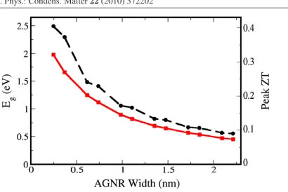
Figure 2.10: Tight binding energy gap (black, circles) and peak ZT (red, squares) as a function of width in ideal AGNRs with indices N = 3, 4, 6, 7, 9, 10, 12, 13, 15, 16, 18, 19. ZT factors values are all evaluated at room temperature (T = 300 K).
of them with AGNR indices N ∼= 0, or 1 (mod 3) are semiconducting, so we evaluated their
thermoelectric properties. Our results reveal that for these semiconducting AGNRs, their
ther-moelectric figure of merit ZT exhibit peaks at the subband edges. In Figure 2.9 shown is a
typical normalized properties plot of the pristine 15-AGNR in the chemical potential range from 0 to 0.5 eVs at room temperature[62]. We then studied a series of semiconducting AGNRs with
different widths and found that their peak ZT positions move towards the center of the energy gap as the widths of the ribbons are increased, while peak ZT values are decreased since wider
ribbons have higher thermal conductance. And similar to the inverse proportionality behavior
of the energy band gap of AGNRs with respect to their widths, we have also identified an approximate inverse proportionality behavior of these peak ZT values with respect to ribbon
widths, as shown in Figure 2.10.
2.3.3 Thermal Transport and Thermoelectrics of GNR Junctions
Graphene nanoribbon junctions and superlattices are very promising candidates for potential nanoelectronic applications [63, 64, 65, 66]. In this subsection, we investigated the thermal
transport and thermoelectrics of GNR semi-infinite junctions utilizing formalisms presented in
Section 2.2.1 and corresponding thermal transport methods in the conductor case scenario. For single interface 4-2 ZGNR and 6-3 AGNR semi-infinite junctions (geometric structures shown in
Figure 2.11: Molecular structures of single interface semi-infinite 4-2 ZGNR junction (a) and 6-3 AGNR junction (b).
as in Figure 2.12. As we can see from these plots that, compared to the ideal bulk
transmis-sion case, the phonon transmistransmis-sion of semi-infinite junctions are quenched everywhere in the whole frequency range due to interface modes mismatches. We also found that the junctional
transmission is not direction-dependent, which is in accordance with the Landauer formalism
within the two-terminal configurations. We calculated phonon transmissions for several GNR semi-infinite junctions, and used Equation 2.21 to calculate their phononic thermal conductance
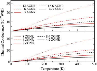
as plotted in Figure 2.13. We can see from the plot that the junction thermal conductance is
always smaller than the narrower part of its components, representing a percentage from 66% to 77% of the narrower components.
Figure 2.13: Upper panel: thermal conductance of 12 AGNR (red dotted), 6-AGNR (red
dashed), 3-AGNR (red solid), 12-6 AGNR semi-infinite junction (black dashed) and 6-3 AGNR semi-infinite junction (black solid). Lower panel: thermal conductance of 8-ZGNR (red dotted), 4-ZGNR (red dashed), 2-ZGNR (red solid), 8-4 ZGNR semi-infinite junction (black dashed) and 4-2 ZGNR semi-infinite junction (black solid).
Thermoelectric properties followed similarly as for the pristine AGNRs case, the only dif-ference is that now both the electronic and phonon transport are calculated using the general
conductor case formalism. Single interface semi-infinite ZGNR junctions do not exhibit any
Figure 2.14: Thermoelectric figure of merit ZT values of 4-2 ZGNR semi-infinite junctions with 5 (solid), 7 (dashed), 9 (dotted) and 11 (dasheddotted) interfaces in the conductor region. The zero in the chemical potential is chosen as the center of the energy gap.
if we increase the number of interfaces in the region between semi-infinite leads, we observe a substantial enhancement of ZT. Figure 2.14 shows ZT for several 4-2 ZGNR semi-infinite
junc-tions with different numbers of interfaces between the leads: the trend in Figure 2.14 shows a
transition from metallic to insulating behaviors simply by adding more interfaces to the central conductor region until saturating at 11 interfaces, a precursor of the behavior observed in GNR
superlattices. On the other hand, most of the semi-infinite AGNR junctions are intrinsically
insulating, provided that at least one end of the junction is insulating. The calculations for the 9-3 AGNR single interface semi-infinite junction give a peak ZT value of 0.2355 at room
temperature. It is important to note that, in such small junctions, the geometry of the bonding itself has a great influence on the ZT value. By making the interface less symmetric (i.e. moving
the narrower end ribbon 3-AGNR more towards the edge of the junction) we observe a drop of
one order of magnitude in the ZT value, a demonstration of the strong geometrical dependence of the thermoelectric behavior in these extremely small GNR junctions. However, if we increase
the widths of the GNRs comprising this interface by three times (27-9 AGNR) we obtain a ZT
Table 2.1: Three highest ZT peak values and their corresponding chemical potential for various AGNR superlattices.
First highest Second highest Third highest
peak peak peak
Superlattice
junction type ZT at µ(eV) ZT at µ(eV) ZT atµ(eV)
6-3 AGNR 0.4777 (1.598) 0.4770 (1.958)
9-3 AGNR 0.5860 (1.430)
12-3 AGNR 0.5979 (1.562) 0.5282 (0.816) 0.5278 (0.974)
15-3 AGNR 0.5520 (0.826) 0.5516 (1.030) 0.3684 (1.784)
18-3 AGNR 0.5906 (1.462) 0.3912 (0.372) 0.3912 (0.510)
21-3 AGNR 0.6144 (1.722) 0.6121 (1.338) 0.5990 (1.524)
24-3 AGNR 0.6005 (1.728) 0.5700 (1.362) 0.5595 (1.530)
27-3 AGNR 0.5516 (1.592) 0.4448 (0.904) 0.4444 (1.054)
30-3 AGNR 0.5842 (1.328) 0.5643 (1.538) 0.3184 (0.596)
12-6 AGNR 0.3902 (0.448) 0.3892 (1.268) 0.3747 (0.772)
18-6 AGNR 0.4044 (0.168) 0.4040 (0.822) 0.4012 (0.450)
24-6 AGNR 0.5542 (1.404) 0.4109 (1.104) 0.4098 (0.756)
30-6 AGNR 0.3710 (0.886) 0.3631 (0.664) 0.3402 (0.478)
36-6 AGNR 0.4079 (1.092) 0.3935 (0.822) 0.3821 (0.478)
42-6 ANGR 0.3503 (0.920) 0.3397 (0.764) 0.2988 (1.316)
48-6 AGNR 0.4425 (1.714) 0.3876 (1.090) 0.3514 (0.604)
54-6 AGNR 0.2772 (1.386) 0.2738 (0.946) 0.2586 (0.826)
60-6 AGNR 0.3620 (1.082) 0.3186 (0.686) 0.3075 (0.902)
18-9 AGNR 0.2576 (0.496) 0.1535 (1.040) 0.1489 (1.142)
27-9 AGNR 0.2548 (0.288) 0.2256 (0.870) 0.2194 (0.498)
36-9 AGNR 0.2378 (0.466) 0.1348 (0.712) 0.1057 (0.898)
45-9 AGNR 0.2982 (1.518) 0.2183 (0.700) 0.2121 (0.322)
54-9 AGNR 0.2875 (1.232) 0.2411 (0.840) 0.1686 (0.434)
63-9 AGNR 0.2163 (0.626) 0.1824 (1.202) 0.1741 (0.320)
72-9 AGNR 0.3452 (1.524) 0.2212 (1.230) 0.2003 (0.690)
81-9 AGNR 0.2471 (1.592) 0.2299 (0.850) 0.1665 (0.574)
Table 2.2: Three highest ZT peak values and their corresponding chemical potential for various ZGNR superlattices.
First highest Second highest Third highest
peak peak peak
Superlattice
junction type ZT at µ(eV) ZT at µ(eV) ZT atµ(eV)
4-2 ZGNR 0.3514 (1.132) 0.1775 (1.540) 0.1748 (1.444)
6-2 ZGNR 0.4360 (1.674) 0.2678 (1.090) 0.0726 (1.204)
8-2 ZGNR 0.7523 (1.098) 0.4592 (1.584) 0.0746 (1.914)
10-2 ZGNR 0.4495 (1.044) 0.4472 (1.446) 0.4451 (1.668)
12-2 ZGNR 0.4562 (1.032) 0.4254 (1.404) 0.4157 (1.566)
14-2 ZGNR 0.4849 (1.016) 0.3579 (1.346) 0.3538 (1.466)
16-2 ZGNR 0.4910 (1.014) 0.4456 (1.794) 0.2678 (1.308)
18-2 ZGNR 0.5061 (1.008) 0.4435 (1.708) 0.1862 (1.278)
20-2 ZGNR 0.4968 (1.008) 0.3694 (1.746) 0.3655 (1.620)
8-4 ZGNR 0.2596 (0.474) 0.2545 (1.886) 0.2444 (1.514)
12-4 ZGNR 0.3734 (1.916) 0.2615 (0.474) 0.2027 (1.358)
16-4 ZGNR 0.2691 (1.952) 0.2619 (0.474) 0.1348 (1.278)
20-4 ZGNR 0.2708 (1.946) 0.2622 (0.474) 0.1684 (1.808)
24-4 ZGNR 0.2853 (1.928) 0.2685 (0.474) 0.0998 (1.490)
28-4 ZGNR 0.2726 (0.474) 0.1478 (1.844) 0.1416 (1.946)
32-4 ZGNR 0.3271 (0.474) 0.2142 (1.858) 0.0717 (1.348)
36-4 ZGNR 0.3269 (0.474) 0.1942 (1.868) 0.0650 (1.132)
40-4 ZGNR 0.3256 (0.474) 0.1542 (1.940) 0.0806 (1.808)
16-8 ZGNR 0.1355 (0.114) 0.0492 (1.662) 0.0238 (0.844)
24-8 ZGNR 0.1381 (0.114) 0.0679 (1.628) 0.0652 (1.790)
32-8 ZGNR 0.1510 (0.114) 0.0689 (1.732) 0.0521 (1.852)
40-8 ZGNR 0.1505 (0.114) 0.0561 (1.816) 0.0535 (1.672)
48-8 ZGNR 0.1503 (0.114) 0.0428 (1.642) 0.0386 (1.738)
56-8 ZGNR 0.1505 (0.114) 0.0338 (1.616) 0.0276 (1.790)
64-8 ZGNR 0.1508 (0.114) 0.0255 (0.838) 0.0231 (1.598)
72-8 ZGNR 0.1515 (0.114) 0.0255 (0.838) 0.0202 (1.432)
Figure 2.15: Highest ZT peaks for AGNR and ZGNR superlattice junctions: (left panel) AGNR superlattice junctions with the narrow end fixed at 3-AGNR, 6-AGNR and 9-AGNR, respectively; (right panel) ZGNR superlattice junctions with narrow end fixed at 2-ZGNR, 4-ZGNR and 8-ZGNR, respectively.
2.3.4 Thermoelectrics of GNR Superlattices
Then we proceed on to calculate the ZT values for a series of AGNR and ZGNR superlattice
junctions using the bulk case formalism with a superlattice periodicity m = 4, which means that there are four hexagons across the longitudinal direction of the smallest repeating unit of GNR
superlattices. Here the thermoelectric figure of merit ZT peaks are still observed in the vicinity
of subband edges of the superlattice electronic band structure. However, the electronic subbands are greatly altered compared with ideal GNRs because of the periodic interfaces present in the
systems. In Tables 2.1 and 2.2 we list the three highest ZT peak values for all the AGNR and
ZGNR superlattices we have investigated. We report only the peak values of ZT and their corresponding chemical potentials µ in the range 0 ∼2.0 eV relative to the reference energy. From these data we can see that peak ZT values of these systems are largely determined by
the index of the smaller end GNRs in the superlattice. An increase in the width of the smaller end decreases the superlattice ZT values. The highest ZT values usually observed are in AGNR
superlattice junctions with the narrowest small end widths. For example, the highest ZT peak
value of 21-3 AGNR is 0.6144 at a chemical potentialµ= 1.722 eV. In Figure 2.15, we plotted the first highest peak ZT values of all these GNR superlattices. Tables 2.1, 2.2 and Figure 2.15
how to determine at which chemical potential the highest peak is achieved even in junctions
with the same small ends. In fact, the change of width ratios changes the electronic subband structure of the superlattice, and thus changes the ZT peak values, which are determined by the
interplay between electronic conductance, Seebecks coefficient and total thermal conductance.
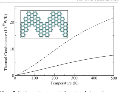
Figure 2.16: Continuous line shows the thermal conductance of a chevron-type GNR (inset) and the dashed line shows the thermal conductance of the same-width straight 9-AGNR.
Finally, we have investigated thermal transport and thermoelectric properties of
chevron-type GNRs as synthesized with an atomically precise bottom-up approach [67]. In Figure 2.16,
we show the thermal conductance of the chevron-type GNR with periodicity 1.7 nm and a pure armchair edge structure, as reported in [67] (see the inset of Figure 2.16). The thermal
conductance of an ideal (straight) 9-AGNR, which is of the same width as the chevron-type
GNR, is plotted for comparison. At room temperature, the thermal conductance of the chevron-type AGNR is reduced to 36% (i.e., a 64% reduction) of that of its straight counterpart. This
reduction is very significant since a lowered thermal conductance associated with good electronic
conductance is a necessary condition for enhanced thermoelectric properties. In comparison, in a 6-3 AGNR semi-infinite junction (see Figure 2.13) the reduction in thermal conductance
induced by the interface was only 34% of the original value for the narrower end. Figure 2.17
Figure 2.17: Electronic transmission (black, dashed) and thermoelectric figure of merit ZT (red, solid) for a chevron-type GNR. The zero in the chemical potential is chosen as the center of the energy gap.
9-AGNR, has a peak ZT value of only 0.145. It is clear that chevron-type GNRs demonstrate a great potential for optimal design of graphene nanostructures with superior thermoelectric
Chapter 3
First Principle Methods and
Localized Wavefunction Basis
In the previous chapter, we have carried out our calculations using model Hamiltonians and
force constant tensors from tight binding methods. There is another major group of methods in
computational science which is known as first principle methods (also calledab initio methods,
usually, we use these two terms synonymously, but there is a tendency that ab initio usually
refers to wavefunction based methods, while first principle refers to density based methods.), which starts from basic principles and does not require fitting parameters. Compared with tight
binding , empirical or semi-empirical methods, first principle methods have several advantages:
• First principle methods do not require fitting (usually to experimental data) , which
increases generality and transferability of the methods.
• First principle methods start from universal physical constants and established basic laws,
there are no a priori assumptions, hence they tend to be very accurate.
• Specific formalisms in carrying out the first principle methods determine the accuracy and applicability of the methods in use, improvements on existing first principle procedures
apply to the underlying formalisms and do not depend on any specific problems in hand.
However, there is one obvious disadvantage of first principle methods compared with tight bind-ing and empirical models. That is, first principle methods are usually much more demandbind-ing in
computational costs than the latter methods. But with the rapid increasing of computational
powers available to researchers today, first principle calculations are becoming more and more affordable. In this chapter and the chapters followed, we investigate and apply the
methods in calculating the electronic structures of molecular or polymeric systems and device
structures. Electronic transport calculations based on first principle electronic structures are also carried out to investigate carrier transport properties through these systems. Our electronic
structure calculations are all considered in the time-independent static Schr¨odinger equation
case under the Born-Oppenheimer (adiabatic) approximation.
3.1
Density Functional Theory Methods
The use of electronic densities as the primary variables to solve quantum mechanical many body problems dated back as early as the 1920s, right after Schr¨odinger’s wavefunction equation was
proposed and is known nowadays as the Thomas-Fermi model. In this model, the kinetic energy
of the electron system is approximated as an explicit functional of the density following idealized models of non-interacting homogeneous electron gas with density equal to the local density at
any given point. Later, Dirac added a local exchange term into the model, hence known as the
Thomas-Fermi-Dirac approximation, and the total energy functional under this approximation is written as [3]:
ET F =T +Vext+VX+VHartree
=C1 Z
d3rn(r)5/3+ Z
d3rVext(r)n(r) +C2 Z
d3rn(r)4/3+1 2
Z
d3rd3r0n(r)n(r 0)
|r−r0| , (3.1)
WhereT is the kinetic energy,Vextis the external potential energy,VXis the Dirac exchange en-ergy, andVHartreeis the classical electrostatic Coulomb energy, with constantsC1= 3/10(3π2)2/3 and C2 =−3/4(3/π)1/3. This model is a precursor of modern density functional theory. The appealing aspect of formulating the quantum mechanical many body problem into one equation
of the electron density functional is that the resulting equation is much more easier to solve than the full Schr¨odinger wavefunction equation which involves the astronomical 3N (∼1023)
degrees of freedom forNelectrons in the system. However, the Thomas-Fermi model has serious
drawbacks, the approximations are too crude to be useful in molecular and solids applications, both the kinetic energy and the Dirac exchange energy terms are not accurate enough, and
many–electron correlation effects are not considered.
The breakthrough came in the 1960s when Hohenberg and Kohn [69] proposed an exact theory of determining all the information of the many body electron system in terms of the
ground state electron density n0(r), and subsequently Kohn and Sham [70, 71] formulated
an ansatz to solve the many body equations approximately. The validations and usefulness of the Kohn-Sham ansatz rests largely on its tremendous success in predicting properties in
atoms, molecules and condensed matter systems. The problem which the Hohenberg and Kohn
Figure 3.1: The Kohn-Sham ansatz reformulation of the many body problem.
Vext(r). In the problems of interacting electrons and fixed nuclei, the electronic Hohenberg-Kohn Hamiltonian can be written as:
ˆ
HHK =− ¯
h2
2me X
i ∇2
i + X
i
Vext(ri) + 1 2
X
i6=j
e2
|ri−rj|
, (3.2)
And the Hohenberg-Kohn (HK) theorems are stated as follows[3],
Theorem 1 For any system of electrons in an external potential Vext(r), that potential is
de-termined uniquely, except for a constant, by the ground state density n0(r).
Theorem 2 A universal functional for the energy E[n] in terms of the density n(r) can be
defined, valid for any external potential Vext(r). For any particular Vext(r), the exact ground
state energy of the system is the global minimum value of this functional, and the density n(r)
that minimizes the functional is the exact ground state density n0(r).
Theorem 1 establishes the uniqueness of the external potential corresponding to a specific
ground state density n0(r), up to an additive constant. With the external potential Vext(r) uniquely determined, the Hohenberg-Kohn Hamiltonian is completely determined, and therefore all the properties of the system for all states (ground and excited) are completely determined
given only the ground state density n0(r). Theorem 2 establishes the existence of a universal total energy functionalE[n] valid for any external potentialVext(r), and by minimizing this total energy functionalE[n] ,the exact ground state energy E0 and densityn0(r) can be completely determined. Proofs of these two theorems are elegant and straightforward by contradictions