Article
Quantitative Imaging of the Stress/Strain Fields and Generation of
Macroscopic Cracks from Indents in Silicon
Brian K. Tanner
1, David Allen
2, Jochen Wittge
3, Andreas N. Danilewsky
4, Jorge Garago
r
ri
5,
Eider Gorostegui-Colinas
6, Reyes M. Elizalde
7and Patrick J. McNally
8*1 Department of Physics, Durham University, South Road, Durham DH1 3LE, U.K.; [email protected] 2 School of Electronic Engineering, Dublin City University, Dublin 9, Ireland. Now at Department of Aerospace,
Mechanical and Electronic Engineering, I.T. Carlow, Ireland; [email protected]
3 University of Freiburg, Kristallographie, Institut für Geo- und Umweltnaturwissenschaften, Freiburg, Germany. Now at Testo SE & Co. KGaA, Lenzkirch Germany; [email protected]
4 University of Freiburg, Kristallographie, Institut für Geo- und Umweltnaturwissenschaften, Freiburg, Germany; [email protected]
5 CEIT and Tecnun (University of Navarra), Paseo de Manuel Lardizabal 15, 20018 San Sebastián, Spain; [email protected]
6 CEIT and Tecnun (University of Navarra), Paseo de Manuel Lardizabal 15, 20018 San Sebastián, Spain. Now at: Lortek, Arranomendi kalea 4A, 20240 Ordizia, Spain ; [email protected]
7 CEIT and Tecnun (University of Navarra), Paseo de Manuel Lardizabal 15, 20018 San Sebastián, Spain.; [email protected]
8 School of Electronic Engineering, Dublin City University, Dublin 9, Ireland; [email protected]
* Correspondence: [email protected]; Tel.: +353 1 7005119
Abstract: The crack geometry and associated strainfield around Berkovich and Vickers indents on silicon have been studied by X-ray diffraction imaging and micro-Raman spectroscopy scanning. The techniques are complementary, the Raman data coming from within a few micrometers of the indentation, whereas the X-ray image probes the strain field at a distance of typically tens of micrometers. For example, Raman data provides an explanation for the central contrast feature in the X-ray images of an indent. Strain relaxation from breakout and high temperature annealing are examined and it is demonstrated that millimeter length cracks, similar to those produced by mechanical damage from misaligned handling tools, can be generated in a controlled fashion by indentation within 75 micrometers of the bevel edge of 200mm diameter wafers.
Keywords: X-ray diffraction imaging; Raman spectroscopy; indentation geometry; plastic deformation; crack generation; plastic deformation strain imaging
1. Introduction
The work described in this paper arose from a detailed study of cracks associated with robotic handling damage in silicon wafers. Catastrophic wafer fracture [1-2] during high temperature processing is a major problem in semiconductor manufacturing with multi-million dollar associated costs on a single production line [3]. At the beginning of our research programme, it was believed that the fracture was associated with cracks introduced by mechanical damage but the location of such damage was not clear. Subsequently the origin of such failure has been shown to be cracks produced at the wafer bevel edge [4-5] due to handling tool misalignment. These cracks can be millimeters in length. Some result in high temperature wafer shattering, while some are benign. As an outcome of our project, commercial X-ray diffraction imaging tools are now available, together with associated analytical software to predict the probability of failure and hence make appropriate decisions relating to the manufacturing process.
As part of the research programme, we used nano-indentation at room temperature to generate cracks in a controlled manner and determine whether such artificially induced cracks could lead to wafer fracture during rapid thermal annealing (RTA). We used scanning electron microscopy (SEM), X-ray Diffraction Imaging (XRDI), also known as X-ray topography, and micro-Raman spectroscopy to study the detailed crack geometry and associated strain fields around Berkovich and Vickers indents. The crack geometry and associated strain fields were studied as a function of indenter load, using a Berkovich tip from 100mN to 600mN and a Vickers tip from there up to 5N. As will become apparent from the results presented below, the cracks generated had high symmetry and in no case were we able to induce wafer fracture during RTA from indents generated away from the wafer edge. Only when the indentation was with a high load and within
approximately 75μm of the bevel edge could millimeter length cracks, such as those now known to induce
catastrophic fracture during processing, be produced. Such indentation-generated cracks sometimes initiated catastrophic fracture during RTA. In this paper we present results of the study of the strain fields around various indentations and explain how the low symmetry bevel edge cracks are generated.
2. Results
In all of the indentation experiments, both with Berkovich and Vickers tips, median surface-breaking cracks were observed to originate at the indenter apices (fig. 1), as was the case in the experiments of Yan et al. [6] for Vickers indents of typically 300-500mN load on InP. Unlike the indentation of InP, however, the crack projections on the surface did not correspond to the intersection of the low surface energy planes which are {111} or {110} in the case of silicon [7]. Rotation of the Bervovich indenter apices with respect to the in-plane crystallographic directions had almost no effect on the crack geometry, the median cracks still emerging almost parallel to the projection of the indenter apices on the surface. For constant indenter load of less than 200mN, the total crack length in the surface remained constant as the indenter was rotated.
Despite the crack extension being only a few microns beyond the indenter impression, the X-ray diffraction images (topographs) [8] were often over a 100μm in extent (fig 2a), demonstrating that the strain field from the defective region is long range. In transmission, the images consisted of two half lobes, with the line of no contrast perpendicular to the projection of the diffraction vector, and a dark central region. The contrast differs from that in the reflection (Bragg) geometry, in which the images consist of a light central region with a complete dark circle at the edge of the contrast area [9]. Although the three images of fig. 2a are all from the same 600mN indenter load, the image length varies significantly for the three images from 139 to 96μm. Such a large dispersion in image size is not observed for loads below about 200mN. On rotation of the indenter tip about the [100] axis, no change in average image dimension was observed (fig 2b). (Note that because of the superposition of the three-fold symmetry of the indenter and the four-fold symmetry of the crystal structure, only a limited range of angle is required to cover all possible angles of rotation.)
Figure 1. Scanning electron microscope image of surface-breaking cracks and associated directions from a 150mN Berkovich indent with the indenter apex parallel to[011].
(a)
(b)
Figure 2. (a)X-ray diffraction image taken in white beam mode of 600mN indents with the indenter tip rotated by 6° with respect to the [011] direction. (b) Extent of the X-ray diffraction contrast for 100mN indents as a function of rotation of the Berkovich tip apex from the [011] direction.
Figure 3. Two dimensional maps of the stress as a function of position around (a) a 600mN and (b) a 400mN indent measured by micro-Raman spectroscopy profiling.The Raman spectroscopy map covers a region whose extent is 30 µm (X) by 50 µm (Y). The red and blue arrows indicate whether the stress is compressive (C) or tensile (T). The highest compressive stress is indicated by the yellow regions, while the greatest tensile strain is indicated by the black/blue regions.
40 60
-10 -5 0 5 10 15
Angle of indenter edge to <011> (degrees)
Image length (
μ
m)
Figure 4. Micro-Raman maps of the stress around the indents shown in fig 3 after annealing for 30 minutes at 1000°C.The Raman spectroscopy maps covers regions whose extent is 30 µm (X) by 50 µm (Y) for fig. 4a and 30 µm (X) by 32 µm (Y) for fig 4b. The red and blue arrows indicate whether the stress is compressive (C) or tensile (T). The highest compressive stress is indicated by the yellow regions, while the greatest tensile strain is indicated by the black/blue regions.
The origin of the loss, in the micro-Raman image maps, of three-fold symmetry, seen in the surface-breaking crack geometry, lies in the presence of breakout above 200mN indent load. An example of such breakout around a 500mN indent is shown in fig. 5. There are two areas of breakout around the three edges of the indenter footprint, as is also the case for the 600mN imprint shown in fig. 3a.
Figure 5. SEM micrograph of a 500 mN Berkovich indent, showing chipping flaws at the edges of the imprint.
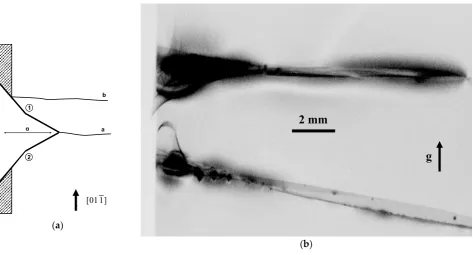
X-ray topograph of fig 6b, long cracks, which again did not propagate on the low surface energy surfaces could be generated by such an indentation technique. Macroscopic crack generation was achieved at a typically 50% success level, it being sensitive to the exact distance of the indent from the bevel edge. These cracks were similar to those generated by repetitive mechanical damage from misaligned wafer handling tools.
(a)
(b)
Figure 6. (a) Schematic diagram of the macroscopic cracks generated by Vickers indentation within 75μm of the bevel edge (b) White beam X-ray topograph of a pair of such cracks. 022 reflection.
3. Discussion
As was evident from a systematic series of experiments with increasing indenter loads, it proved impossible to generate macroscopic cracks in silicon when the indent was far from the wafer edge. In all cases, the crack lengths were limited to several micrometers, the median surface breaking cracks always being initiated at the indenter apex. Unlike conical indents [10,11], where it was found that {110} cracks were mainly introduced from the indent, indicating that fracture occurs most easily along the {110} planes among the crystallographic planes of the <001> zone, with Berkovich indents we found no association of the crack geometry with the low surface energy planes. Indeed, ultra-fast X-ray diffraction imaging of fracture in silicon has recently shown that even when cracks are apparently following low energy {110} surfaces, there is a continual jumping between {110} and {111} planes [12].
The limit on the length of crack is primarily determined by breakout associated with lateral cracks intersecting the surface. When breakout occurs, the strain is relaxed and further crack propagation does not occur. We have noted elsewhere that there is strong asterism in X-ray topographs when breakout is about to
occur [9].Lateral cracks were always found to be present even at low indenter loads when breakout did not
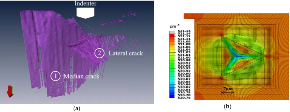
occur. An example is shown in fig. 7a in the case of a 120mN load indent where breakout did not occur. This is a three-dimensional reconstruction from a sequence of images taken during focused ion beam milling of the sample. We have shown that finite element (FE) modelling reproduces the shape of the main median crack rather well [9] when cohesive elements are included to represent the relaxation from cracking. The presence of varying length lateral cracks, explains the breaking of the symmetry in Raman strain maps of low load indents even when breakout does not occur. Without the stochastic nature of the lateral cracking process, the FE simulations always show three-fold symmetry, even to the highest loads. An example is shown in fig 7b, which is a simulation that does not include cohesive elements. We note, however, that the simulation shows stress concentration at the tips of the indenter, which is where the median cracks are initiated and, as in the experimental images of fig. 3, a tensile strain is predicted directly below the indenter apex.
[110] a α
β
1
2
b
] 1 01 [
(a) (b)
Figure 7. (a) 3D reconstruction of subsurface cracks corresponding to a 120 mN Berkovich indent, showing one of the three median cracks (1) and a lateral crack (2). (b) Simulation of the shift of the Raman TO phonon line for a 750mN indent.
Due to the high strain sensitivity of X-ray diffraction imaging, the localized symmetry breaking is not reflected in the geometry of the X-ray images of the strain fields around the indents. The X-ray images form at typically 30μm distance from the indent where the strain level is relatively low and the long range strain field is still nearly symmetric. When breakout occurs, the long range strain field falls in magnitude and the X-ray contrast begins to occur at a smaller distance from the indent. It does not, however, significantly change its symmetry (fig 2a). The line of zero contrast, perpendicular to the diffraction vector direction, arises because the contrast only arises from displacement components in the diffraction vector direction. Along the horizontal line through the center of the indent, the strain field is entirely in the horizontal direction; there is no component in the diffraction vector direction. There is thus no contrast along this line, giving rise to the two lobes in the image. The difference between the image widths parallel and perpendicular to the diffraction vector arises from a diffraction contrast effect. The diffraction vector lies in the incidence plane, which also includes the entrance and exit beams. So-called ‘direct’ or ‘kinematical’ contrast [13], such as seen here, forms at a point when the effective misorientation of the deformed lattice exceeds the perfect crystal diffraction, or Darwin, width. For deformation greater than this, the region selects a slightly different wavelength which diffracts kinematically and additional intensity appears locally in the image. However, the X-ray beams from this region have a different Bragg angle and the diffracted wave therefore travels in a different direction in space. Due to the large distance, typically 300-400mm, between the sample and detector the image is spread out as the propagation distance increases. No such magnification takes place in the direction perpendicular to the incidence plane (or diffraction vector) and hence there is a difference in the width in the two directions. The absence of change in the dimensions of the image as the indenter orientation is changed confirms the symmetry of this long range strain field.
As was pointed out by Tang et al. [14], discontinuity in the unloading curve referred to as pop-out, does not signify the appearance of cracks and the 3D reconstructions from all samples studied showed the presence of lateral as well as median cracks (fig. 7a). During the loading stage, below the indenter, normal diamond cubic structure Si-I phase material is transformed to the metallic β-Sn phase Si-II. On subsequent unloading, the transformation of the Si-II phase to body center cubic (bc8) Si-III and rhombohedral (r8) Si-XII phases is associated with the pop-out phenomenon, though the size and position of the discontinuity is related to the maximum load and the unloading rate [15]. In all indents at and above 150mN load, below which the stress level was apparently not sufficient to transform Si-I to Si-II on loading, micro-Raman spectra taken after indentation reveal lines attributable to the Si-III and Si-XII phases. Our loading/unloading data is entirely consistent with previous work [16-17]. Further, in all samples thinned and studied by scanning transmission electron microscopy, we have observed a region of plastic deformation below the indent [9] such as has been associated [18-19] with the pop-in discontinuities which we also observed during loading.
The factor of four reduction in the maximum compressive stress and the loss of the tensile stress below the indenter point, following high temperature annealing, is associated with nucleation of dislocation loops from the indentation site at temperatures where Si is ductile [20]. As illustrated in the X-ray section topograph of fig. 8a, taken with a 15μm wide entrance slit, the dislocation loops lie on the inclined {111} slip planes and propagate right through the 750μm thick wafer. Depending on the profile of the temperature gradients within the annealing furnace, the loops propagate in one or both of the two orthogonal <011> directions in the wafer plane. The loops subsequently thicken into slip bands by a process of cross-slip, the early stages of which are illustrated in fig. 8b. Dislocation nucleation and propagation relieves the short range stress around the indent, imaged in the micro-Raman profiles.
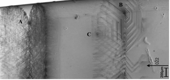
An example of how very quickly the individual X-ray diffraction images of dislocations become indistinguishable during the process of slip band development is given in fig. 9. This shows two indents of the
same load of 500mN, close to the bevel edge, following an anneal for 60 seconds at 1000°C. (The varying
thickness on the bevel gives rise to the almost horizontal thickness fringes at the top of the image, this being a well-known dynamical X-ray diffraction effect.) The indent A on the left, probably having experienced a stronger temperature gradient, has a well-developed slip band within which, although some dislocations can still just be resolved, most dislocation images cannot be individually distinguished. In contrast, the slip band development in the right hand image B is much less developed and the operation of a source of dislocation loops can be identified. As the loop expands, driven by the stress around the indent and the thermal gradient in the furnace, the 60° segment parallel to the interface glides out of the crystal and the screw and other 60° segments glide on the inclined {111} slip planes. The dislocation images are narrow where the dislocation intersects the exit surface of the wafer with respect to the X-ray beam and the elegant interference fringes that decorate the broadening image of the dislocation towards the X-ray entrance surface constitute the so-called intermediary image. This is a dynamical diffraction effect sometimes seen under conditions of moderate absorption, such as here. The dislocation loop originating from C, and interfering with the development of the slip band from indent B, arises from handling damage on the wafer surface. It has very similar characteristics to the effect of the indents, generating its own loop system that is developing into a slip band.
quantitative measure of the back stress which counters the opening and propagation of a crack [4]. A narrow
image width D indicates a small back stress, potentially leading to an unstable crack. Using the Griffith
criterion, it is straightforward to show that when κ exceeds a critical value κc , i.e. when
κ = L/D > κc (1)
the crack will propagate during processing at high temperatures. Whether a particular crack is, or is not, benign depends on the temperature profile of the specific furnace and calibration is necessary to determine relevant κc in order to use the model predictively.
The upper crack shown in Fig 6(b) was similarly benign due to its low κ value, but the lower and longer of the two cracks resulted in wafer fracture. Although not shown here, the image of the tip of the lower crack is very narrow and as the crack is long, the κ value is high. Under the particular annealing conditions, κ > κcand the wafer fractured.
(a)
(b)
Figure 8. (a) X-ray section topograph of slip dislocations generated on {111} glide planes from surface indentations upon annealing. (b) X-ray diffraction image of the early stages of cross slip leading to thickening of the dislocation loops into a slip band and nucleation of the orthogonal slip systems.
Figure 9. X-ray diffraction image of early stage slip band generation from two adjacent indents close to the bevel edge of the wafer.
A
B
C
]
2
02
[
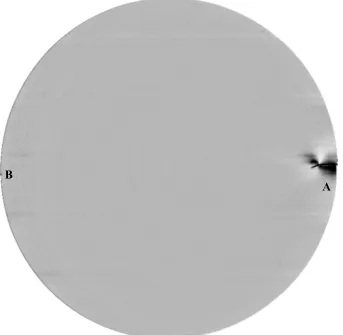
Figure 10. X-ray diffraction image, taken on a prototype of the Bruker/Jordan Valley QCTT wafer imaging tool, of two edge indents, one (A) of which generated a macroscopic crack in the 200mm diameter wafer (right) and one (B) which did not nucleate such a crack (left).
4. Materials and Methods
All experiments were performed on (100) oriented, integrated circuit quality, dislocation-free, 200mm diameter silicon wafers purchased from Y Mart Inc, Palm Beach Gardens, Florida, USA. Wafers were within 0.2° of (100) orientation. The nominally defect-free, double side polished, p-type wafers had resistivity below 10 ohm mm, and were of thickness 725 (±25) μm. No edge defects were visible either under optical inspection or in X-ray diffraction images of the as-received wafers, which had been packed and shipped in standard cassettes.
Two pieces of indentation equipment were used to generate controlled damage on silicon. The first was a
Nanoindenter® II from Agilent (formerly Nano Instruments Inc., USA), used to indent at low loads (100mN to
600mN), and the second was a Mitutoyo AVK-C2 hardness tester, used for application of heavier loads from
500mN up to 50N. A Berkovich tip, was used with the Nanoindenter® II. It was a three-sided diamond
pyramid with each face making an angle of 65.35° with the indenter axis, with a total included angle of 142.3°. The Mitutoyo AVK-C2 had a Vickers tip which was a four sided diamond pyramid, with a total included angle of 136º, but the same projected area-to-depth as the Berkovich indenter. All indents were performed at room temperature. Scanning electron microscopy was performed on a field emission electron microscope (LEO 1525) with an in-lens secondary electron backscattering detector.
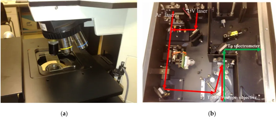
Micro-Raman spectroscopy was used to measure the strain and crystalline damage as well as high pressure phase transformations produced by the nano-indentation. The system used in this study was a
Jobin-Yvon Horiba HR800® system running LabSpec 5 software and integrated with a microscope coupled
confocally to an 800mm focal length spectrometer (fig. 11a). Samples were mounted on a high precision table capable of x-y and z translation. A diffraction grating of 1800 groves per millimetre was used to split the
Raman signal into individual wavelengths, which were then directed onto a CCD detector. The HR800 uses two different CCD detectors; an air cooled Synapse CCD system and a liquid nitrogen cooled CCD3000 system used for acquisition times of greater than 120 s. Three lasers are connected to the Raman system
through a periscope: a Uniphase 2014 488nm Argon ion (Ar+) visible laser with a maximum output power of
20mW, a Spectra-Physics Stablite 2017 364nm Ar+ UV laser with a max. output power of 100mW and a
Kimmon Koha IK3201IR-F 325nm Helium Cadmium (He-Cd) ultraviolet (UV) laser with a max. output power of 22.4mW.
For the μRS measurements a backscattering geometry was used. In this configuration a microscope
objective is used to focus the beam onto the sample surface and the system is equipped with a number of lenses allowing different optical magnifications and can produce spot sizes as small as 1-3 µm in diameter (fig. 11a). Scattered light is collected through the same objective and passes through a beam splitter and is focused on to the entrance slit of the spectrometer which disperses the light onto one of the CCD detectors (fig. 11b). The use of a flip mirror enables the specimen under the microscope objective to be visualised using a small camera, which is particularly useful for precise positioning of the laser beam onto the area of interest.
(a) (b)
Figure 11. (a) Microscope lenses attached to the LabRam® HR800 System. The sample under test typically sits on a glass microscope slide below the objective lens. (b) Internal light paths for LabRam® HR800 System. The red line shows the path of the laser beam, while the green line shows the path of the Raman scattered beam.
The spectrometer was centred on the Raman line of the TO Raman phonon peak shift for unstrained silicon at 520.07 cm-1 [21]. Assuming the strain in the indented silicon to be biaxial, the stress components σxx
and σyy are equal and related to the spectral line shift by
GPa yy
xx 04 1
ω ω σ
σ = = − (2)
where
ω
0 is the wavenumber (in cm-1) of the unstrained Raman spectral line of the Si–Si transverseoptical (TO) phonon and
ω
1 is that of the measured Raman spectral line of the sample. Long scans requiredfor 2D Raman maps can take from a number of hours to a number of days to complete. In order to compensate for temperature and laser stability the plasma lines of the laser were recorded as fidiucal markers over the entire duration of the scan. The laser plasma lines are Rayleigh scattered and thus are insensitive to any strain in the sample [21]
of ~0.025 cm-1/K), erroneously implying the presence of a tensile strain. However, this shift [22]is smaller than
the resolution of the spectrometer used in this study.
X-ray diffraction imaging was performed in white beam mode at the TOPO-TOMO beamline at the ANKA synchrotron radiation source at Karlsruhe, Germany and at beamline B16 of the Diamond Light Source at Didcot, Oxford, U.K. At ANKA, transmission images were recorded on a CCD camera optically coupled to a macroscope and with a Lu3Al5O12 scintillator. The effective pixel size of the detection system was
2.5 × 2.5 μm. At the Diamond Light Source, transmission images were recorded with a CCD camera
manufactured by PCO.Imaging GmbH, which has 4008 × 2672 pixels and a 14 bit dynamic range. Scintillators
and objective lenses were chosen such that the pixel size effective (binned) pixel size was 2μm. Data
acquisition times were between 10 and 40 s. All transmission diffraction images were taken with the 022 reflection, oriented such that there was a principal wavelength of 0.0506 nm. Further details of the ANKA instrumentation can be found in reference [23].
Scanning electron microscopy (SEM) was performed on a field emission electron microscope (LEO 1525) with an in-lens secondary electron backscattering detector. A Quanta 3D dual beam FIB from FEI, which incorporates FEGSEM (field emission gun scanning electron microscopy) and FIB (focused ion beam) cannons, was used to make microscopic observations of cracks around indents as the specimen was FIB
milled down. The electron and ion beam cannons form an angle of 52° to each other. The instrument
incorporated SE (secondary electron), BS (backscattered electron) and STEM (scanning transmission). From the FIB cross sections, three-dimensional reconstruction of the cracks was achieved using Amira reconstruction software. Simulation of the crack geometry was performed using the commercial software ABAQUS (version 6.8-3). The code incorporates a cohesive zone model and a simple triangular relation between stress and crack face separation was used.
5. Conclusions
Micro-Raman and X-ray diffraction imaging both provide maps of the strain field around indentations but on substantially different length scales. In particular, the symmetry associated with the indenter profile is lost in the X-ray images whereas the micro-Raman maps reveal in detail not only the magnitude and sense of the strain field but also its detailed symmetry. This is particularly revealing when breakout occurs. On annealing, the strain field maximum moves away from the site of the indent due to the formation of a series of dislocation loops, which are the precursors of slip bands. By exploiting the symmetry breaking of the beveled edge of the wafer, i.e. by indentation close to the wafer edge, we have been able to generate macroscopic cracks in 200mm wafer in a controlled, though not always predictable, manner.
Acknowledgments: Financial support was provided through the European Community FP7 STREP project SIDAM (Grant No. FP7-ICT-216382). Technical support from Kawal Sawhney, Igor Dolbnya and Andrew Malandain at beamline B16 of the Diamond Light Source and P. Vagovic, T. dos Santos Rolo and H. Schade at ANKA (Angströmquelle Karlsruhe) is gratefully acknowledged. Thanks are extended to Keith Bowen for valuable discussions and initially conceiving the SIDAM project. Financial support was provided through the European Community FP7 STREP project SIDAM (Grant No.216382). Funds for open access publication came from Dublin City University.
Author Contributions: BKT, RME, PJM and AND collaboratively conceived and supervised the experiments within the research programme framework, which was coordinated by BKT; JG performed most of the indentations; CE undertook SEM observations and analysis; DA undertook micro-Raman analysis; EGC made finite element simulations of the strain fields; BKT, PJM, AND, DA, JS and JG undertook X-ray diffraction imaging experiments; BKT wrote the first draft of the paper
References
[1] Chen, P.Y., Tsai, M.H., Yeh, W.K., Jing M.H. and Chang, Y., Investigation of the relationship between whole-wafer strength and control of its edge engineering, Japan. J. Appl. Phys.2009 48, 126503
[2] Chen, P.Y., Tsai, M.H., Yeh, W.K., Jing M.H. and Chang, Y. Relationship between wafer edge design and its ultimate mechanical strength Microelectronic Eng.2010 87, 2065-2070
[3] Atrash, F., Meshi, I., Krokhmal, A., Ryan P., Wormington, M. and Sherman, D., Crystalline damage in silicon wafers and 'rare event' failure introduced by low-energy mechanical impact, Mater. Sci.in Semicond. Processing201763 40–44 [4] Tanner, B. K., Fossati, M. C., Garagorri, J., Elizalde, M. R., Allen, D., McNally, P. J., Jacques, D., Wittge, J. and Danilewsky A. N., Prediction of the propagation probability of individual cracks in brittle single crystal materials, Appl. Phys. Lett.2012101 041903
[5] Tanner, B. K., Garagorri, J., Gorostegui-Colinas, E., Elizalde, M. R., Bytheway, R., McNally, P. J. and Danilewsky A. N., The Geometry of Catastrophic Fracture during High Temperature Processing of Silicon, Int. J. Fracture2015195 79-85. [6] Yan, J., Tamaki, J., Zhao H.W. and Kuriyagawa, T. Surface and subsurface damages in nanoindentation tests of compound semiconductor InP, J. Micromech. Microeng. 2008 18 105018
[7] Tanaka, M., Higashida, K., Nakashima, H., Takagi, H. and Fujiwara, M.Orientation dependence of fracture toughness measured by indentation methods and its relation to surface energy in single crystal silicon Int. J. Fracture2006139 383– 394.
[8] Bowen, D. K. and Tanner, B. K., X-ray Metrology in Semiconductor Manufacturing, CRC Taylor and Francis, Boca Raton 2006 pp 279 +xi
[9] Tanner, B. K., Garagorri, J., Gorostegui-Colinas, E., Elizalde, M. R., Allen, D., McNally, P. J., Wittge, J., Ehlers, C. and Danilewsky, A. N., X-ray Asterism and the Structure of Cracks from Indentations in Silicon, J. Appl. Cryst. 201649 250-259 [10] Tanaka, M., Higashida, K., Nakashima, H., Takagi, H. and Fujiwara, M. Fracture toughness evaluated by indentation methods and its relation to surface energy in silicon single crystals, Mater. Trans. 2003 44 681-684
[11] Tanaka, M., Higashida, K., Nakashima, H., Takagi, H. and Fujiwara, M. Orientation dependence of fracture toughness and its relation to surface energy in Si crystals J. Japan. Inst. Metals2004 68 787-791
[12] Rack, A., Scheel, M. and Danilewsky, A. N. Real-time direct and diffraction X-ray imaging of irregular silicon wafer breakage IUCrJ2016 3, 108–114.
[13] Bowen, D. K. and Tanner, B. K., High Resolution X-ray Diffraction and Topography, Taylor and Francis, London 1998
pp 252 + x
[14] Tang, Y., Yonezu, A., Ogasawara, N., Chiba, N. and Chen, X ., On radial crack and half-penny crack induced by Vickers indentation, Proc. Roy. Soc. Lond. A 2008 464, 2967-2984
[15]Chang, L. and Zhang, L. C., Deformation mechanisms at pop-out in monocrystalline silicon under nanoindentation, Acta Mater. 2009 57, 2148-2153
[16] Bradby, J. E., Williams, J. S. and Wong-Leung, J., Transmission Electron Microscopy Observation of Deformation Microstructure under Spherical Indentation in Silicon, Appl. Phys. Lett.2000 77, 3749-3751
[17] Gerbig, Y.B., Stranick, S.J., Morris, D.J., Vaudin, M.D. and Cook, R.F., Effect Of Crystallographic Orientation On Phase Transformations During Indentation Of Silicon, J. Mater. Res. 2009 24, 1172-1183.
[18] Bradby, J. E., Williams, J. S., Wong-Leung, J., Swain, M. V. and Munroe, P., Mechanical deformation in Silicon by micro-indentation, J. Mater. Res. 2001 16, 1500-1507
[19] Bradby, J.E., Williams, J.S. and Swain, M.V. In situ electrical characterization of phase transformations in Si during indentation, Phys. Rev. B2003 67, 085205
[20] Wittge, J., . Danilewsky, A. N, Allen, D., McNally, P., Li, Z., Baumbach, T., Gorostegui–Colinas, E., Garagorri,J., Elizalde, M. R., Jacques,D., Fossati, M. C., Bowen, D. K. and Tanner, B. K., Dislocation sources and slip band nucleation from indents on silicon wafers, J Appl Cryst2010 43, 1036-1039
[21] De Wolf, I. Micro-Raman spectroscopy to study local mechanical stress in silicon integrated circuits Semicond. Sci. Technol. 199611, 139-154
[22] DombrowskiK.F., PhD thesis Micro-Raman investigation of mechanical stress in Si device structures and phonons in SiGe, Brandenburg University of Technology, Cottbus-Senftenburg, 2000
![Figure 2. (a)by 6 X-ray diffraction image taken in white beam mode of 600mN indents with the indenter tip rotated ° with respect to the [011] direction](https://thumb-us.123doks.com/thumbv2/123dok_us/8030762.1336320/3.595.63.543.295.473/figure-diffraction-image-indents-indenter-rotated-respect-direction.webp)