ISSN(Online): 2319-8753 ISSN (Print): 2347-6710
International Journal of Innovative Research in Science,
Engineering and Technology
(An ISO 3297: 2007 Certified Organization)
Website: www.ijirset.com
Vol. 6, Issue 6, June 2017
Performance Analysis of a Low Voltage Power
Efficient Dynamic Comparator
Sweta Snehi 1, Ashwani Kumar 2
P.G. Student, Department of Electronics and Communication Engineering, IGDTUW, Kashmere Gate, Delhi, India1
Professor, Department of Electronics and Communication Engineering, IGDTUW, Kashmere Gate, Delhi, India2
ABSTRACT: Analog to Digital Converters are essential for recovering digital signals from analog signals as processing of digital signals is found to be much easier and safe for transmission of information. This makes an ADC essential for applications such as wireless communication and signal processing. In today’s semiconductor industry, priority is laid upon designing low-power circuits that can work at lower supply voltages. For this many low power techniques have been investigated. Used as a fundamental block in most ADC architectures, comparators with low-power and reduced delay are essential for faster operation of ADCS. In this paper, a dynamic comparator has been proposed that meets the requirement of high-speed and low-power without any added complexity. A comparative analysis has been presented in terms of various parameters that include power, delay, energy, power-delay product and kickback noise. The simulation is carried out in 0.18um CMOS technology at 0.8V supply using Cadence Virtuoso design environment.
KEYWORDS: Conventional dynamic comparator, Double tail dynamic comparator, High-speed ADCs, Low power, Kickback noise.
I. INTRODUCTION
In today’s VLSI industry, millions of transistors are placed on a single chip. This leads to increased power dissipation producing unwanted heat in the circuits. For cooling down of the chip, extra circuits must be incorporated that makes it expensive and denser. The most crucial task in today’s VLSI industry is to reduce this power consumption and design circuits for higher speed of operations. To meet the requirement of power and speed, supply voltage is scaled down with each technology. This requires that the threshold voltage be scaled down with the same pace. But this is not achieved and a limitation is put on scaling down the supply voltage. Analog to Digital Converters (ADCs) employ comparators as their basic building blocks. Thus designing a comparator that meets the requirement of low-power and high-speed and can work at the lower supply voltages has become essential. For high speed operation of ADCs like Flash ADC, comparators with lower power consumption and working at higher speed is required. For this purpose dynamic comparators or clocked comparators are utilized. Positive feedback or latch regeneration process enhances the performances of comparator in terms of power and operation speed and are widely used in designing high-speed ADCs [2].
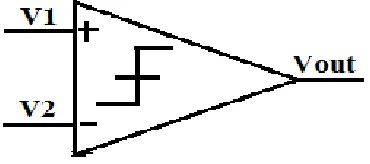
Comparator is an electronic device with two input terminals. Either voltage or current is provided at its input terminals. It compares the voltage or current values present at its input terminals and produces an output indicating which one among the two inputs is greater. The comparator that compares currents at its input is a current comparator and the one that compares voltages is a voltage comparator. In an ADC, the comparator is fed with sampled signal which then gives the equivalent digital output of the corresponding sampled signal.
ISSN(Online): 2319-8753 ISSN (Print): 2347-6710
International Journal of Innovative Research in Science,
Engineering and Technology
(An ISO 3297: 2007 Certified Organization)
Website: www.ijirset.com
Vol. 6, Issue 6, June 2017
Fig. 1. Symbol of a comparator
CMOS dynamic regenerative comparators are widely known for their fast-speed, low power, high input impedance and rail to rail output swing. They use positive feedback mechanism with one pair of back-to-back cross coupled inverters (latch) in order to convert a small input-voltage difference to a full-scale digital level in a short time [2].
In this paper a dynamic comparator with much reduced power consumption and higher speed is proposed. The simulation is done using Cadence Virtuoso tool in GPDK 180nm technology. The kickback noise of the comparator is also calculated and it is found that the value is reduced for the proposed comparator.
The rest of this paper is arranged as follows. Section II presents schematic and operation of dynamic regenerative comparators. The proposed comparator is presented in section III. Section IV describes the Kickback noise and its schematic for calculation. Simulations and results are presented in section V. Section VI addresses the conclusion.
II. DYNAMICREGENERATIVECOMPARATORS
The latch regeneration due to the cross-coupled inverters generates positive feedback forcing fast decision making in the circuit. A clock regenerative comparator is a circuit which brings out decision according to the input signal which is either high or low at every clock cycle [1].
A. Conventional Dynamic Comparator (Single Tail Comparator):
The schematic of conventional dynamic comparator is shown in fig. 3 [9]. The advantage of this structure is rail to rail output swing, no static power consumption, high input impedance and less affected by noise [4]. The drawback of this circuit is requirement of larger number of transistors due to several stacked transistors makes the circuit larger.. This also causes larger delay. A larger tail current is required for fast regeneration in the latch [3].
The operation of conventional dynamic comparator can be divided into two phases, reset phase and decision-making phase. In reset phase, when CLK=0, the tail transistor, NM0 turns off and reset transistors, PM0 and PM3 turn on. The output nodes Outn and Outp are then charged to VDD. A valid logic level is thus obtained during reset phase defining a start condition.In decision-making phase (comparison phase), when CLK=VDD, the tail transistor, NM0 turns on and reset transistors PM0 and PM3 turn off. The output nodes that have been already charged to a definite value equivalent to logic 1 begin to discharge with different rate of discharge. The rate of discharge depends upon the corresponding input voltages, INN and INP. If VINN > VINP, outp discharges quicker than outn. When the voltage at Outp reaches to a value equal to VDD-|Vthp| before Outn, the corresponding pMOS transistor PM turns on. This will charge the output
node, Outn to VDD which will in turn make the transistor NM4 to turn on and thus discharge the output node Outp to ground. This process is the latch regeneration process caused by the back-to-back connected inverters (PM1, NM3 and PM2, NM4) [4].
ISSN(Online): 2319-8753 ISSN (Print): 2347-6710
International Journal of Innovative Research in Science,
Engineering and Technology
(An ISO 3297: 2007 Certified Organization)
Website: www.ijirset.com
Vol. 6, Issue 6, June 2017
Fig. 3. Schematic of dynamic conventional comparator.
B. Conventional Double Tail Comparator
The schematic for conventional double tail comparator is shown in fig 4 [9].
ISSN(Online): 2319-8753 ISSN (Print): 2347-6710
International Journal of Innovative Research in Science,
Engineering and Technology
(An ISO 3297: 2007 Certified Organization)
Website: www.ijirset.com
Vol. 6, Issue 6, June 2017
The difference between conventional dynamic comparator and conventional double tail dynamic comparator is that the double tail comparator can operate at lower supply voltage as compared as compared to conventional dynamic comparator [3]. The schematic for conventional double tail comparator is shown in fig. 4 [7].
The operation of this comparator is executed in two phases. In reset phase (CLK=0), tail transistors (PM4 and NM8) are off. Transistors PM2 and PM3 charge the nodes fn and fp at the drain terminals of these transistors to VDD. As a result of this charging event the intermediate stage transistors, NM11 and NM12 turn on discharging the output nodes (Outn and Outp) to ground.
During comparison phase when CLK=VDD, tail transistors, PM4 and NM8 turn on. PM2 and PM3 transistors are cut-off . The voltages at fn and fp nodes begin to drop at different discharge rates. This voltage drop depends mainly on the drain current of tail transistor (NM8) and the load capacitance value at fn and fp nodes. As in conventional dynamic comparator, the delay of this comparator comprises charging capacitive delay and latch regeneration delay. The disadvantage of this circuit is that it consumes more power. The proposed circuit overcomes this drawback.
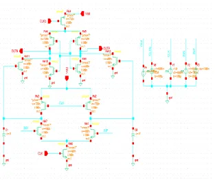
C. Modified Double Tail Comparator [1]:
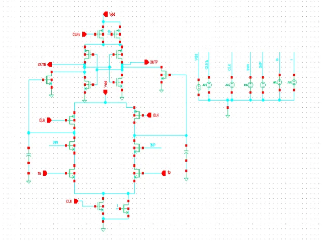
The circuit proposed in [1] as shown in fig. 5 is a modified version of conventional double tail comparator. In this paper, this modified version has been further modified for high speed and low-power. The proposed circuit is shown in fig. 6. The kickback noise calculation is also done for both these circuits and it is calculated to be lower for the proposed circuit.
Fig. 5. Schematic of double tail comparator as proposed in [1].
The working of the comparator shown in fig. 5 is described as follows. During RESET phase (CLK=0) tail transistors turn off. The voltages at nodes fn and fp are both pulled up to VDD. Intermediated stage transistors reset both output nodes outn and outp toVDD.
During decision-making phase (CLK=VDD), tail transistors turn on. The voltages at nodes fn and fp begin to fall in
ISSN(Online): 2319-8753 ISSN (Print): 2347-6710
International Journal of Innovative Research in Science,
Engineering and Technology
(An ISO 3297: 2007 Certified Organization)
Website: www.ijirset.com
Vol. 6, Issue 6, June 2017
The modification was done by inserting two control transistors for faster latch regeneration. Although the circuit is improved in terms of operation speed and thus energy per conversion, the kickback noise is increased in comparison to conventional double tail comparator [1]. The proposed comparator in this paper will improve the circuit in fig. 5 in terms of power, speed, energy and even kickback noise.
III.PROPOSED COMPARATOR
The schematic of proposed double tail comparator is shown in fig. 6. In the proposed circuit, the control transistor as was added in the proposed circuit of [1], is removed and two extra transistors are added parallel to the two tail transistors connected between the power rail and the rest of the circuit.
The main idea behind the proposed comparator is to reduce the time period for which the circuit is on. For this two transistors are added as can be seen in fig. 6. The inputs provided to these transistors are pulse voltages which have reduced on time period. This leads to reduction in power and enhances the speed of the proposed circuit.
Fig. 6. Schematic of proposed double tail comparator.
IV.KICKBACKNOISE
ISSN(Online): 2319-8753 ISSN (Print): 2347-6710
International Journal of Innovative Research in Science,
Engineering and Technology
(An ISO 3297: 2007 Certified Organization)
Website: www.ijirset.com
Vol. 6, Issue 6, June 2017
Fig. 7. Circuit to evaluate kickback noise.
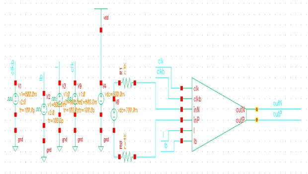
The circuit used for evaluation of kickback noise is shown in fig. 7 [12]. The preceding stage is modelled as Thevenin equivalent circuit. In this paper, the value of RTH is taken to be 8KΩ for simulations
Fig. 7. Kickback noise calculation for circuit shown in fig. 5.
. A circuit has been implemented to calculate the kickback noise of the comparators, shown in fig.7 and fig. 8.
ISSN(Online): 2319-8753 ISSN (Print): 2347-6710
International Journal of Innovative Research in Science,
Engineering and Technology
(An ISO 3297: 2007 Certified Organization)
Website: www.ijirset.com
Vol. 6, Issue 6, June 2017
V. SIMULATIONSANDRESULTS
Fig. 9. Transient response of conventional dynamic comparator.
For the efficient comparison of proposed comparator with the comparator proposed in [1] as shown in fig. 5, all the circuits are simulated in 180nm CMOS technology at power supply voltage of 0.8V and clock frequency of 50MHZ.
ISSN(Online): 2319-8753 ISSN (Print): 2347-6710
International Journal of Innovative Research in Science,
Engineering and Technology
(An ISO 3297: 2007 Certified Organization)
Website: www.ijirset.com
Vol. 6, Issue 6, June 2017
Fig. 11. Transient response for the comparator in fig. 5.
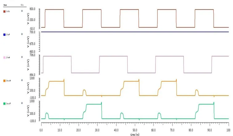
The transient response of the comparator as proposed in [1] and the transient response of the modified comparator is shown in fig. 11 and fig. 12 respectively. The value of capacitance for both the simulations is kept at 1fF.
Fig. 12. Transient response for proposed comparator.
ISSN(Online): 2319-8753 ISSN (Print): 2347-6710
International Journal of Innovative Research in Science,
Engineering and Technology
(An ISO 3297: 2007 Certified Organization)
Website: www.ijirset.com
Vol. 6, Issue 6, June 2017
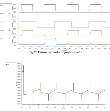
The output waveform corresponding to the calculation of kickback noise is shown in fig. 13 and fig. 14. The spikes in the output waveform are the kickback noise voltage levels. The difference between the initial point and the final point of the spikes is calculated as the kickback noise voltage. As can be seen from the voltage waveform, the kickback noise in the proposed comparator is found to be reduced. The RTH value is 8KΩ and the Thevenin voltage is 700mV.
Fig. 14. Waveform for kickback noise calculation of fig. 8.
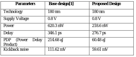
Different parameters like power, delay PDP and kickback noise has been calculated and tabulated below.
TABLE I. RESULT COMPARISON
Parameters Base design[1] Proposed Design
Technology 180 nm 180 nm
Supply Voltage 0.8 V 0.8 V
Power 620.3 nW 218.6 nW
Delay 346.1 ps 276.7 ps
PDP (Power Delay Product)
214.68 aJ 60.48 aJ
Kickback noise 111.62 mV 59.61 mV
VI. CONCLUSION
In this paper, a modification of dynamic comparator has been presented. The designed circuit has been verified using 0.18um CMOS technology at VDD=0.8V. Analysis of the parameters like power, delay, power-delay product and kickback noise .A circuit topology for calculating kickback noise has also been presented. The proposed comparator is found to be faster and dissipating lesser power with reduced kickback noise value.
REFERENCES
[1] S. Babayan-Mashhadi and R. Lotfi, "Analysis and Design of a Low-Voltage Low-Power Double-Tail Comparator," in IEEE Transactions on Very Large Scale Integration (VLSI) Systems, vol. 22, no. 2, pp. 343-352, Feb. 2014.
[1] A. Rabiei, A. Najafizadeh, A. Khalafi and S. M. Ahmadi, "A new ultra low power high speed dynamic comparator," 2015 23rd Iranian Conference on Electrical Engineering, Tehran, pp. 1266-1270, 2015.
[2] S. S. Chiwande and S. P. Akarte, "Performance analysis of low voltage, low power dynamic double tail comparator for data convertor application," 2016 World Conference on Futuristic Trends in Research and Innovation for Social Welfare (Startup Conclave), Coimbatore, pp. 1-4, 2016.
ISSN(Online): 2319-8753 ISSN (Print): 2347-6710
International Journal of Innovative Research in Science,
Engineering and Technology
(An ISO 3297: 2007 Certified Organization)
Website: www.ijirset.com
Vol. 6, Issue 6, June 2017
[4] Lahariya, Aparna, and Anshu Gupta. "Design of Low power and high speed dynamic latch comparator using 180 nm technology." Signal Processing, Computing and Control (ISPCC), 2015 International Conference on. IEEE, 2015.
[5] S. B. Gawhare and A. Gaikwad, "Area and power efficient high speed voltage comparator," 2016 International Conference on Automatic Control and Dynamic Optimization Techniques (ICACDOT), Pune, 2016, .
[6] D. Schinkel, E. Mensink, E. Klumperink, E. van Tuijl and B. Nauta, "A Double-Tail Latch-Type Voltage Sense Amplifier with 18ps Setup+Hold Time,"IEEE International Solid-State Circuits Conference. Digest of Technical Papers, San Francisco, CA, 2007, pp. 314-605,2007.
[7] Majumder, Alak, et al. "Design of low noise high speed novel dynamic Analog Comparator in 65nm technology." Radioelektronika (RADIOELEKTRONIKA), 2016 26th International Conference. IEEE, 2016.B. Goll and H. Zimmermann, "A Comparator With Reduced Delay Time in 65-nm CMOS for Supply Voltages Down to 0.65 V," inIEEE Transactions on Circuits and Systems II: Express Briefs, vol. 56, no. 11, pp. 810-814, Nov. 2009.
[8] H. Patil and M. Raghavendra, "Low power dynamic comparator for 4 — bit Flash ADC," IEEE International Conference on Computational Intelligence and Computing Research (ICCIC), Chennai, India, 2016, pp. 1-4, 2014.
[9] M. P. Dev, D. Baghel, B. Pandey, M. Pattanaik and A. Shukla, "Clock gated low power sequential circuit design,"2013 IEEE Conference on Information & Communication Technologies, JeJu Island, pp. 440-444, 2013.
[10] P. M. Figueiredo and J. C. Vital, "Kickback noise reduction techniques for CMOS latched comparators," inIEEE Transactions on Circuits and Systems II: Express Briefs, vol. 53, no. 7, pp. 541-545, July 2006.
[11] A. Majumder, M. Das, B. Nath, A. J. Mondal and B. K. Bhattacharyya, "Design of low noise high speed novel dynamic Analog Comparator in 65nm technology," 2016 26th International Conference Radioelektronika (RADIOELEKTRONIKA), Kosice, pp. 115-120, 2016.
![Fig. 5. Schematic of double tail comparator as proposed in [1].](https://thumb-us.123doks.com/thumbv2/123dok_us/1602461.1198050/4.595.131.473.401.660/fig-schematic-double-tail-comparator-proposed.webp)