Abstract
AMSINCK, CHRISTIAN JOHANNES. Molecular Electronic Memories. (Under the direction of Paul Damian Franzon.)
The feasibility of building large memories using molecular electronic devices with bistable conductance-state memory has been investigated. A novel fabrication method for two-terminal molecular memory devices that is integrateable into large-scale arrays while avoiding top-contact evaporation on a molecular monolayer has been developed. A sacrificial layer underneath the top contact metal is wet-etched to create free-standing cantilevers in aqueous solution and a self-assembled monolayer is formed on the underside of the cantilever. Subsequent atmospheric drying causes the freestanding structure to become permanently adhered to the substrate, resulting in a two-terminal molecular structure. This device has been investigated with alkanethiol monolayers as a proof-of-concept, and the expected decrease in current with increasing chain length is observed. The measured current density in control devices without molecules is also consistent with models of loaded cantilevers. Previously characterized molecules exhibiting memory behavior were also investigated and demonstrated bistable memory effects similar to earlier observations.
The scalability of such bistable molecular memory devices was analyzed from a circuits perspective, and the impact of different system parameters was quantified. It is necessary to build large arrays with at least several hundred molecular memory cells along each
dimension, in order to prevent peripheral circuitry from dominating the area. It is quantitatively shown how this requirement constrains the minimum allowable
Molecular Electronic Memories
by
Christian Johannes Amsinck
A dissertation submitted to the Graduate Faculty of North Carolina State University
in partial fulfillment of the requirements for the Degree of
Doctor of Philosophy
Electrical Engineering
Raleigh 2006
APPROVED BY
______________________________ ______________________________
Biography
Christian Johannes Amsinck, son of Reinhard and Gabriela Amsinck, was born in Bamberg, Germany on June 4, 1980. Raised partly in the vicinity of Bamberg and later Aschaffenburg in Germany, he moved to Montreal, Canada in 1995 and graduated from the Alexander von Humboldt German School high school in 1997. After attending
Acknowledgements
First of all, I praise and give thanks to God who gave me the strength, endurance and courage to keep going many times throughout my life as a Ph.D. student through various personal and professional crises. Allowing me the opportunity to obtain the highest degree is both an incredible privilege and gift, as well as a responsibility in a world where so many people never learn to read and write. I hope I will live up to His purpose. He also
surrounded me with many people in my life who in various ways made this possible for me. My parents and my sister – without your steadfast support and encouragement, this would simply not have been possible. Letting me vent when an experiment didn’t work or
cheering when I finished writing a chapter, I could always count on you being there for me through thick and thin – although you probably wonder when the “thin” was…
Paul Franzon – who probably spoiled me as a boss for life, giving me freedom to explore so long as I made progress, offering a helping hand whenever anything stagnated, and even giving me free flying lessons!
Veena Misra, John Muth and Greg Parsons – whose advice and help was invaluable to me in staying focused on the important and on the feasible.
Neil Di Spigna – besides meticulously proofreading and improving just about anything I ever wrote, you were always willing to make time to discuss the latest failed experiment and/or play devil’s advocate to help me find solutions. I hope you never decide to go to law school…
David Nackashi – you first helped me get my feet under myself and make progress up the learning curve when I started in this area and smoothed out the paths as the first in our moletronics triumvirate.
Sachin Sonkusale – who had a knack for helping me make progress by asking me those insightful (and often annoyingly inconveninent) questions.
The folks at NRL, particularly Jason Lazorcik, Ratna, Shash, Amy Blum, Jim Kushmerick, Steve Pollack and Marty Moore – thank you for your insights, encouragement,
understanding and help during the Viral NanoBlock project. I really enjoyed those trips going up to NRL, I learned so much every time, and you all showed a lot of patience with a computer engineer who was clueless about why his proposed circuits might be a slight bit challenging to build.
Jim Tour, Bo Chen, Jianli He and Jacob Ciszek – for letting me wreak havoc in your lab and helping me, especially with the stiction experiments.
Within Paul’s research group, John Damiano, Steve Lipa, Steven Mick, John Wilson, Dave Winick – all of you contributed in various ways.
At the Analytical Instrumentation Facility – Rich Fiore, Dale Batchelor and Mike Salmon – for helping me learn SEM and AFM.
Michele Joyner – who was my secret weapon on the fourth floor and beyond many times.
Table of Contents
List of Tables ...viii
List of Figures...ix
1 Introduction...1
Historical Overview...1
Dissertation Outline...2
2 Literature Review...4
Chemistry ...6
Theoretical Physics...8
Experimental Physics ... 15
Mechanically Controlled Break Junctions... 15
Structures with evaporated top contact on SAM... 17
Scanning Probe Microscopy ... 20
Crosswire Testbed... 22
Proximal Probes... 23
Architecture... 24
Conclusion ... 27
3 Stiction Testbed ...29
Motivation ... 29
Stiction Process... 31
Processing Steps ... 31
Choice of Substrate ... 34
Thermal Oxidation ... 34
First-level Photo (Liftoff Stack) ... 34
Electron-beam Metal Evaporation... 35
Liftoff ... 35
Second-level Photo... 36
Undercut Etch ... 36
Transfer Under Immersion... 37
Photoresist Strip ... 38
Molecular Self-Assembly ... 39
Drying... 40
Characterization... 42
Optical ... 42
Electrical... 44
Substrate Contact Resistance... 44
Yield... 46
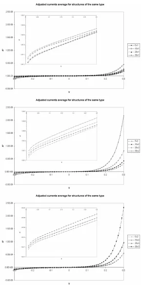
Current-Voltage Measurements... 50
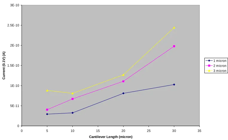
Control Samples without molecules – correlation with cantilever geometry... 50
Experimental Results... 50
Theoretical Evaluation of the Physical Structure ... 54
Defining the Correct Conditions for Sticking of Single-clamped Cantilevers... 55
Calculating Real Contact Area ... 57
Current Density Analysis ... 70
Theoretical Description of Current Transport ... 73
Alkanethiol Samples – correlation with molecular character (chain length) ... 75
Experimental Results... 77
Theoretical Description of Current Transport ... 79
Molecular Barrier Height/Width... 79
Bipyridyl-dinitro samples – Molecular Memory Effects... 83
Experimental Results... 85
Current Density Comparison... 88
Repeatability ... 89
Longevity... 94
Burn-In and Multiple State Behavior... 95
Integration ... 98
Conclusion ... 99
4 Molecular Memory Scalability ...102
Motivation ... 102
Outline ... 104
Molecular Memory Model... 105
Crossbar Architecture... 109
Operation... 113
Write Operations ... 114
Reset ... 114
Write1 ... 115
Read Operation ... 116
Readout Margin Definition ... 117
Optimal Load Resistor Derivation ... 118
HSPICE Netlist Generation Methodology... 119
Finding the worst-case ... 121
Reset ... 122
Write1... 127
Read ... 129
Evaluation in terms of the readout margin... 132
Senseamp Sensitivity... 134
Noise ... 134
Device variation ... 135
Read scalability... 138
Scalability Argument... 142
Theoretical analysis of large-scale arrays ... 144
Ladder circuit approximation ... 144
Inductive ∆-Y bounding ... 147
Circuit model... 150
Scalability arguments using the circuit model ... 151
Negligible interconnect impedance... 152
Derivation of readout margin... 152
Conclusion ... 158
5 Conclusion ...161
Novel Claims and Future Work ... 161
Stiction vs. Top-Contact Evaporation ... 161
Demonstration of Memory Effect ... 161
Stiction Integration into Crossbar Arrays ... 161
Scalability of Molecular Crossbar Memory Arrays ... 162
6 References...163
Appendices ...173
Appendix A: HSPICE Model of Molecular Memory Element ... 174
List of Tables
Table 3-1: Processing steps (traveler) for the stiction structure ...32
Table 3-2: Yield versus geometry of the cantilever for a sample experimental run of 19 total structures of each type measured (228 structures total) ...49
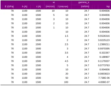
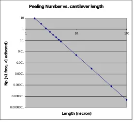
Table 3-3: Peeling bounds for various cantilevers ...56
Table 3-4: Equilibrium average surface distance d0 and corresponding normalized contact area A*...66
Table 3-5: Measured current densities vs. expectation from theory...72
Table 3-6: Calculated barriers for alkanethiol structures...82
Table 3-7: Molecular assembly step for BPDN molecule...84
Table 3-8: Measured Current Density Values from [Blum2] compared to experimental results ...89
Table 3-9: Switching characteristics across different devices...92
Table 3-10: Switching behavior of a single device over 40 cycles ...95
Table 4-1: Peripheral circuitry area overhead as a function of memory array size (µm2) .104 Table 4-2: Crossbar memory parameter definitions ...112
Table 4-3: Default parameters for crossbar memory ...113
Table 4-4: Summary of reset, write and read operations ...114
Table 4-5: Equivalent resistances of molecular device during reset operation ...115
Table 4-6: Equivalent resistances of molecular device during write1 operation ...115
Table 4-7: Equivalent resistances of molecular device during read operation...117
List of Figures
Figure 3-5: Image of a down cantilever using interference microscopy. The stuck-down part has a different color (red in this case) than the probe pad (grey-green) due to the height difference ...43 Figure 3-6: Substrate contact using alligator clips showing repeatability ...45 Figure 3-7: Pedestal technique used to probe shards with alligator clips grounding the substrate...46 Figure 3-8: Different cantilever types: (A) L type, (B) S type ...46 Figure 3-9: A part of the probe pad that is difficult to control is stuck down on S Type cantilevers. The images are taken on different samples from the same experiment, the right sample shows a much larger portion of the probe pad stuck down than the left...47 Figure 3-10: Rapid undercut of the cantilever in the etchant ...47 Figure 3-11: Bent cantilever resulting from large currents during blow-dry step...48 Figure 3-12: Pinhole defects cause large areas of the probe pad to stick down, affecting the device yield...48 Figure 3-13: Correlation of zero-bias conductivity with cantilever geometry. The three curves show data for 1, 2, and 3 micron wide cantilevers, respectively...51 Figure 3-14: Correlation of current with cantilever geometry. The three curves show data for 1, 2, and 3 micron wide cantilevers, respectively ...51 Figure 3-15: Current-voltage characteristics for different cantilever geometries ...53 Figure 3-16: Cartoon of the types of forces acting on a cantilever in the process of sticking down...54 Figure 3-17: Peeling number vs. Cantilever length ...57 Figure 3-18: Capillary condensation threshold for Au-Si system ...62 Figure 3-19: Equilibrium average surface distance d0 and corresponding normalized contact
Figure 3-21: Force (per unit area) balance between the attractive (van-der-Waals, capillary) and repulsive (microhardness) forces. Equilibrium is reached when the repulsive force (red) equals the attractive forces (green). ...69 Figure 3-22: Real contact area as a function of equilibrium distance d0. For the calculated d0
of 55Å, the real contact area A* is 4.7% of the apparent contact area. ...69 Figure 3-23: Current density vs. voltage for Au-Si for different substrate doping
(reproduced from [Chang1])...70 Figure 3-24: Currents at 0.1V for 1 micron wide cantilevers of various lengths and linear fitting of the data to give linear current density...71 Figure 3-25: Experiment 16-May-05 data and linear fit ...73 Figure 3-26: Rectifying current-voltage characteristics observed for the stiction structures for control, C10 and C16 samples (inset: log scale) ...77 Figure 3-27: Trends of the current level with respect to cantilever geometry and molecular chain length ...78 Figure 3-28: Forward-bias current-voltage characteristics on a log scale for a C16 sample 80 Figure 3-29: Γ calculated from the exponential fits of the I-V characteristics ...81 Figure 3-30: Inconsistent I(0) as a basis for barrier calculation, comparing three
experimental runs. Top: May 16, Middle: June 7, Bottom: August 31 ...83 Figure 3-31: Dithiol BPDN molecule ...83 Figure 3-32: BPDN switching characteristics. The I-V traces exhibit a jump in conductivity on the increasing-voltage sweep at a larger voltage, and a drop during the
Figure 3-37: Longevity testing of a memory device for 40 cycles. The first cycle is at the bottom, the 10th cycle second from bottom, 20th cycle third, 30th cycle second from top and 40th cycle on top...94 Figure 3-38: Voltage stressing - "burn-in" - of the structure could be used in most cases to successfully created a memory device if the initial behavior was erratic. The bottom curve shows the first trace, subsequent traces result in the stable memory device shown in the top four traces ...96 Figure 3-39: An apparent three-state device ...97 Figure 3-40: Crossbar concept using stuck-down cantilever array (top left: before sacrificial layer etching, top right: after etching, molecular assembly and stick-down, bottom: crossbar array of stuck-down cantilevers over orthogonal wires)...98 Figure 4-1: Limitation of functional density by the peripheral circuitry in arrays of
insufficient scale ...103 Figure 4-2: Model of bistable molecular memory device featuring two conductivity states in the forward bias region...106 Figure 4-3: Current-voltage sweep of the parameterizable molecular memory device model
...107 Figure 4-4: Internal circuit of the molecular memory device model...108 Figure 4-5: Example fabrication process for molecular crossbar memory: (1) fabrication of wire array, (2) molecular assembly on wires, (3) fabrication of crosswire array, (4)
passivation ...110 Figure 4-6: Molecular memory crossbar structure (4x4 shown) ...111 Figure 4-7: Beneficial effect of resetting devices on resets further along the wordline ....123 Figure 4-8: Impact of resistance values (normalized to their default values given in Table 4-3) on Reset...124 Figure 4-9: Effect of interconnect impedance and array size on %VM vs. (a) the number of wordlines [n] (b) the number of bitlines [m] ...125 Figure 4-10: %VM during Reset in a square RAM (m=n) for different interconnect
Figure 4-11: Impact of resistance values (normalized to their default values given in Table 4-3) on Write1 operation ...128 Figure 4-12: %VM during Write1 in a square RAM (m=n) for different interconnect
impedances ...129 Figure 4-13: VOUT for different memory state scenarios as a fraction of VWA-VBA – the
accessed cell being closest to the drivers on the top 4 rows, and farthest from the drivers on the bottom 4 rows ...132 Figure 4-14: Readout margin defines noise immunity, specifications of senseamp
sensitivity and tolerance on device variability of molecular devices ...133 Figure 4-15: Effect of readout margin RM and the variability parameter β on the
probability of an error during the worst-case read operation ...137 Figure 4-16: The probability of incorrect operation of a worst-case read as a function of quality factor β...138 Figure 4-17: Impact of resistance values (normalized to their default values given in Table 4-3) on Read operation...139 Figure 4-18: Effect of interconnect impedance and array size on %RM vs. (a) the number of wordlines [n] (b) the number of bitlines [m]...141 Figure 4-19: %RM during Read in a square RAM (m=n) for different interconnect
impedances ...142 Figure 4-20: Crossbar memory array ...143 Figure 4-21: Transformation of a wordline to the resistive ladder approximation...146 Figure 4-22: Iterative transform of the line through repeated use of the ∆-Y transformation
Figure 4-27: Required on/off ratio as a function of the number of words in the memory (different curves are labeled by the corresponding %RM) ...155 Figure 4-28: Lack of scalability for symmetric memory devices (different curves are
1
Introduction
Historical Overview
Since Richard Feynman’s famous challenge that “there’s plenty of room at the bottom” on December 29th, 1959, nanotechnology has come a long way. Scientists and engineers have made tremendous progress towards fabricating ever smaller features, as well as inventing tools to probe and image the world at scales approaching atomic size.
In the mid 1990’s, a research program aiming to investigate the electronic conduction properties of a single molecule was founded, culminating in several landmark papers showing not only electrical conduction through a molecule, but all manner of interesting properties ranging from molecular rectification to negative differential resistance and even bistable memory [Chen2, Reed2]. These results generated a great amount of excitement in the scientific community, and a tremendous research effort was set into motion to utilize these newly discovered molecular-scale effects for building a molecular computer as an exercise to scale computing beyond the eventual limits of complementary metal-oxide-semiconductor transistors.
Simultaneously with the groundbreaking experimental work, theoretical physicists attempted to model these effects such as negative differential resistance and two-state behavior. However, while the basic principles of molecular conduction were coming to be understood, the methodology and assumptions used in theoretical models of the more interesting NDR and memory/switching effects remained both difficult as well as
controversial. Nevertheless, continued efforts to wire up a molecular computer resulted in small circuits being honored as Science’s “Breakthrough of the Year” [Service1]
[Service2]. From this critical review, however, promising smaller-scale results emerged as scientists refocused on understanding the underlying principles completely before
launching ambitious system-building efforts. Exhaustive studies showed that at least some molecule-based conductivity switching exists in certain molecules [Blum2], as thorough studies on simpler molecules [Wang1] were performed to examine the detailed conduction mechanisms present in these molecular junctions.
Dissertation Outline
In chapter 2, a literature review puts this work into context with the current state of the art of molecular electronics. The core field of molecular electronics are examined, including chemistry (both synthetic and surface chemistry), theoretical physics and current transport modeling, experimental physics and molecular electronic characterization and finally computing architectures using molecular electronic components. Roughly half of the novel claim of this thesis largely pertains to test and characterization within molecular electronics and an overview of the existing methods to characterize molecular electronic conduction. The other half pertain to integration of molecular electronic memories into large systems, and the available physical and logical architectures are also treated in detail.
In chapter 3, the stiction test and integration structure is described in detail. The motivation stemming from the need for an integrateable molecular two-terminal device structure is explained, followed by a detailed description of the concept and physical structure of the stiction structure. The molecule-less experiments used to validate the candidacy of this structure as a molecular testbed are described and compared to a mechanical analysis of the forces in the system to verify that the behavior of the structure is well-understood.
Experimental results with alkanethiol monolayers assembled in the molecular junction are analyzed, showing the stiction concept is a valid approach to building a molecular
electronics device. A molecule of great practical interest showing memory effects in various other test structures is inserted into the structure, and memory effects are observed and described.
molecular memories with insignificant peripheral circuitry overhead, the need for large-scale integration is quantified. After exploring the detailed operation of such a conductivity-based molecular memory and the worst-case conditions under which the performance parameters need to be examined, a detailed scalability analysis based on the readout margin is performed. This analysis yields both the device and integration structure characteristics that will be necessary to build a large-scale array of molecular memory elements efficiently and reliably.
2
Literature Review
Back in the mid 1970’s, when integrated silicon technology was still in its relative infancy, a farsighted paper by Aviram and Ratner [Aviram1] proposed that certain kinds of
molecules, if subjected to an electrical field along their axis, would not allow current to pass equally well in one direction as in the other, and exhibit a nonlinear, rectifying
behavior. For the next 25 years, constant development on the processing techniques used to manufacture ever denser and faster transistors on silicon made smaller and smaller feature sizes accessible. Moore’s law, the trend of transistor density doubling every 18 months, has led to reduced gate lengths of integrated transistors to around 0.1µm today [Maruccio1, Kagan1]. Laboratory experiments and special techniques are capable of producing even smaller features. Also, microscopy technology has been developed to allow resolving features on the single-molecule size domain with the invention of the scanning-tunneling microscope [Binning1] in 1981, and later, the atomic force microscope.
The advent of these technologies has renewed interest in the original Aviram and Ratner paper, since early attempts to study the electrical properties of organic molecules
[Henisch1, Potember1, Aviram2] were hindered by the sheer difficulty of accessing the single-nm domain necessary to investigate them. In addition, predictions by the silicon manufacturing industry [Sematech1] indicate that several fundamental physical limitations will impose an end on the continued shrinking of the MOSFET structure. Contrary to roadblocks encountered in the past, these are not merely technological difficulties that can be circumvented by introducing new processing technologies such as dopant implant or shorter-wavelength lithography. Fundamental physical limits threaten to put an end to the continuation of Moore’s law. Thermodynamics dictates that the energy needed to write a bit must exceed several kT to prevent bit errors (thermal limit), the Heisenberg uncertainty principle limits the product of bit energy and read/write frequency (quantum limit), and the economical cooling of the heat dissipated during operation is only feasible up to a certain point (power dissipation limit) [Maruccio1].
of the device characteristics on the location of individual dopant atoms become dominant [Ghosh1]. In addition, leading edge semiconductor manufacturing already requires fabrication plants costing tens of billions of dollars, and this cost is forecast to vastly increase with further downscaling of feature sizes, presenting an economical barrier to further scaling as well. All this implies that there exists a minimum size for a functional MOS transistor that the silicon community is forecast to reach at some time between 2010 and 2016 [Sematech1]. Therefore, it is important to study the conduction behavior of molecules and small clusters, and to search for a device in which quantum mechanical effects are the operational principle instead of a detrimental side effect, motivating the field of molecular-scale electronics [Reed3].
Due to the mesoscopic nature of the research, it has been suggested [Marrucio1] that research teams had best take a very multidisciplinary approach. Thus, this effort has been led by teams using a remarkably collaborative approach between theoretical and
Figure 2-1: Structure of relationships in the collaborative research effort in molecular electronics In the following sections, the results and relevance of each of these subunits in the overall context of molecular electronics research will be discussed.
Chemistry
In a sense, the versatility of the carbon atom is the foundation of molecular electronics. The rich variety of molecules that can be synthesized using organic chemistry relatively quickly and inexpensively [Kagan1] is a major reason for the interest in the field. In fact, synthetic chemists have already succeeded at fabricating molecules intended to be the functional equivalent of insulators, wires, rectifiers, switches of various types, even transistors, memory elements and sensors [Kagan1, Ghosh1, Joachim1, Tour2]. Large oligomers featuring extended π-conjugation of precise length and constitution have been synthesized for applications as molecular wires, including oligo(phenylene-ethynylene)s and
substituting the hydrogens with amino and nitro moieties, in order to obtain redox-active molecules expected to have nonlinear current-voltage characteristics [Tour2]. Molecules with a donor-bridge-acceptor complex (similar to the original Aviram-Ratner concept) attached to a long alkyl chain were synthesized, and rectifying characteristics were observed on Langmuir-Blodgett mono- and multilayers [Metzger1, Metzger2]. With the hope of observing conductivity switching effects, rotaxane molecules with bistable configurations were synthesized [Balzani1] and assembled in a tunnel junction [Luo1, Collier1]. Chiropticene [Parakka1] and metal complex [Dei1] chemistry were also
employed toward the endeavor of obtaining a molecular memory/sensor device. In theory, by controlling the electronic structure of the molecular core, whether by sidegroup
functionalization, modulation of chemical bonding, or other means, it is possible to control the through-molecule transport, and build different devices with the same alligator clip moiety [Xue1]. This also allows the “design” of molecules with specific features for hypothesis testing [Weber1], for example, to test for/against the presence of specific conduction/switching mechanisms [Price1, Seminario2].
Despite the ability to tailor molecules, it still remains difficult to envision synthesizing large and complex organic molecules such as envisioned by Ellenbogen et al. [Ellenbogen1] that aim to integrate the electronic functionality of an entire logic block, like a binary adder. Self-assembly, especially hierarchical self-assembly of small building blocks is a more feasible strategy towards obtaining molecular electronic building blocks [Wu1]. To a large degree, the discovery of self-assembly by surface chemists, especially sulfur-based assembly chemistry on noble metals [Nuzzo1, Bain1] has inspired the bottom-up approach underlying molecular electronics. Instead of fabricating structures by reducing larger structures to the nanoscale (e.g. thin-film processing), it is envisioned that
hierarchical self-assembly will be a much cheaper and accessible route to manufacture mesoscale objects [Ellenbogen1, Stan1, Wu1]. The most common system used is the thiol “alligator clip” binding the organic molecules to gold [Schreiber1], with the hydrogen released upon chemisorption [Whitesides1], the most energetically favorable configuration binding the sulfur at the center of 3 close-spaced gold atoms on the Au-111 surface
combinations has been investigated using density-functional theory and [Seminario3] and it was found that the highest conductivity should be achieved using Pd instead of Au, and that using isocyanide [Chen2] or selenol [Vuillaume1] instead of thiol alligator clips may be advantageous depending on the molecule [Seminario3, Kushmerick4]. Thiol-Au is used mainly for historical reasons, but is likely a suboptimal material combination due to the nonideal coupling and somewhat uncertain contact geometry [Kagan1, Yaliraki1]. The ability of the thiol endgroup to bind to many different metals [Schreiber1] presents a challenge as well, making it difficult to force a specific orientation of an asymmetric molecule in a given system. Even though most molecular devices have only two termini due to the enormous difficulty of fabricating three or more contacts separated by distances on the molecular scale [Xue1, Stan1], attachment specificity would still be required to prevent mirror images of the desired geometry. Careful design of the assembly conditions is also required in each case to achieve the desired structure [Stapleton1].
In summary, chemists have succeeded at synthesizing a host of candidate molecules for molecular electronics and developed attachment chemistries and self-assembly strategies suitable for integration into molecular devices. While chemists develop the necessary synthesis approaches, the electronic structure of the devices are generally designed in collaboration with quantum physicists according to their theoretical predictions of interesting effects due to specific features of the electronic structure of the molecule.
Theoretical Physics
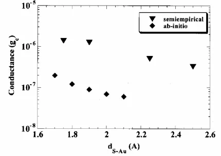
used by most researchers is to describe the nonequilibrium transport through a Green’s function technique (non-equilibrium Green’s function NEGF), and to combine this with a formal treatment of the molecular energy states through extended Hückel modeling, density functional theory (DFT) or other formalisms and solving for a self-consistent solution [Ghosh1]. This approach has been widely used to investigate the conduction mechanism through molecular “wires”, although there is some debate about the methods that should be employed for the molecular description. Ratner et al. show that the semi-empirical extended Hückel (EH) modeling approach gives results for molecular conductivity which are
significantly different from their own ab-initio calculations on the Hartree-Fock level of theory (see Figure 2-2: Conductance dependence of the α-α' xylyl dithiol system on molecule-electrode separation. Reprinted from [Yaliraki1]. Copyright (1999), American Institute of Physics.), for both a benzene-1,4-dithiol and α,α’ xylyl dithiol molecule chemisorbed between two gold contacts [Yaliraki1].
Thus it is not clear how reliable the EH method is for predicting conductivities, although it may be useful in correctly predicting trends [Yaliraki1, Tian1].
Nevertheless, density functional theory (DFT) has also been scrutinized with regards to the appropriateness of applying it to molecular electronics calculations. The Hartree-Fock level of theory commonly used in DFT calculations usually predicts a too-large HOMO-LUMO gap as it includes the gas-phase, isolated-molecule one-electron charging energy that may not be appropriate for structures closely coupled to the metal electrodes [Tian1]. Also, Reimers et al. found [Reimers1] that modern DFT breaks down systematically in four separate areas related to long-range electron correlation: dispersion, charge transfer, extended π-conjugation and bond cleavage. Most commonly used modern density functionals underpredict HOMO-LUMO bandgaps, are unreliable in predicting the
evaluation of the HOMO to the Fermi level as well as in predicting the screening of applied fields, and may calculate the system geometry incorrectly when dispersive forces are
atoms at either end) and the tight-binding method for the contacts, they calculate the
electronic structure lining up as shown in Figure 2-3: Energy level diagram and band lineup of benzene-1,4-dithiol on Au. Reprinted from [Xue1].
Figure 2-3: Energy level diagram and band lineup of benzene-1,4-dithiol on Au. Reprinted from [Xue1]. Copyright (2001), American Institute of Physics.
Figure 2-4: Electrostatic potential distribution in a molecular junction. Reprinted from [Tian1]. Copyright (1998), American Institute of Physics.
While for small biases and small molecules, it may be appropriate to consider the molecule as a constant potential with the entire potential drop occurring across the contacts [Tian1], longer molecules and larger biases require a more detailed investigation of the electrostatic profile. Here also, as well as in the Fermi level lineup, the metal contacts to the molecule have a large impact on the behavior of the modeled device [Adams1, Vuillaume1], even qualitatively: Introducing an asymmetry factor η, Tian et al. showed that asymmetric coupling to the contacts produces strongly asymmetric characteristics even for symmetric molecules [Tian1]. The stronger the molecule is coupled to the contacts – a prerequisite for high current densities and reliable devices – the greater the intermixing of molecular orbitals and metal states [Adams1]. In this way, the study of molecules to a certain extent will always be limited to being somewhat “system-level” tests, since molecular
characteristics are not independent of the contacts.
the alligator-clip region, suggesting that molecular functionality can be developed somewhat independent of the choice of metal/alligator clip [Xue1].
With the evolving understanding of molecular transport, different conduction mechanisms have been identified to produce the rectifying behavior initially proposed by Aviram and Ratner [Aviram1]. One is based on the idea of superexchange, a coherent tunneling process, which has exponential dependence on the separation distance, where the tunneling occurs through the molecular orbitals, mediated by virtual oxidized/reduced states of the donor-bridge-acceptor complex [Adams1].
The second mechanism is based on the idea of hopping conduction, where the charge carrier actually resides on the bridge, possibly completely delocalized, and the D+B–A or DB+A– states are real [Adams1]. In chemical reactions in solution both electron transfer mechanisms are, in general, present simultaneously, but even in a metal-molecule-metal junction, it is necessary to differentiate between the tunneling and ballistic transport mechanisms, as well as other, parasitic mechanism like thermionic emission and impurity conduction. This can be accomplished by performing temperature-dependent measurements [Adams1]. Scientists at Yale led by Mark Reed measured the conduction through
dodecanethiol between 80K and 300K, and were able to confirm that direct tunneling conduction is the dominant transport mechanism in their system [Wang1, Lee1], as would be suggested by the lack of delocalized orbitals in the alkanethiol molecule.
In the same study, the exponential decrease of the conductivity with distance in the
tunneling regime was analyzed [Wang1], by using different-length alkanethiols with 8, 12 and 16 carbon atoms, respectively. A theoretical study for different-length linear
In addition to the rectifying and conductive/isolating behaviors that can be described on this level of theory, several mechanisms have also been put forward in an attempt to account for the switching behavior and negative differential resistance (NDR) observed experimentally [Joachim1, Chen1, Bozano1, Reed2, Bandyopadhyay1, Rawlett1].
Proposals for explaining experimental observations of NDR have included a two-step reduction process, where the mono-anion has enhanced conductivity compared to the neutral molecule, which it loses upon further reduction with a second electron under
increased bias [Chen1, Seminario1]. Very similar molecules in a different testbed, however, have shown to exhibit statistical conductivity switching behavior that was attributed to conformational changes [Donhauser1]. In a different experiment, memory effects and NDR was observed as well, and explained by a mechanism involving the filling of
charge-trapping levels setting up a space charge which opposes the applied field and reduces current [Bozano1, Chen2].
A mechanism based on the mechano-chemical circumrotation of two interlocked circular molecules when one of the two is oxidized has been put forth to explain the reversible switching observed in rotaxanes [Collier1, Collier2]. However, control experiments performed in a similar structure show the switching behavior to be qualitatively independent of the type of molecule [Stewart1]. These results have cast doubt on the circumrotation mechanism as the origin of the switching effect, and the formation of nanoscale filaments has been suspected to be the source of a great deal of confusion in this area [Bozano1, Stewart1]. Nevertheless, theoretical studies [Kornilovitch1, Kornilovitch2] have shown that conformational mechanisms do hold promise for building bistable
molecular switching elements.
lineup and improved numerical methods, it is necessary to build testbeds with both known as well as reproducible configurations, so that different effects can be isolated from each other as much as possible. Experiments need to be devised that allow theoreticians to gain insight into all the different and mutually interacting factors impacting molecular transport separately, before they can construct a comprehensive model with full explanatory and predictive power.
Experimental Physics
The major bottleneck to progress in molecular electronics remains in the area of
characterization [Kushmerick4]. Due to the small scale, it has proven difficult to not only create structures that allow for measuring the current through a single molecule or at least a small number of molecules [Zhou1], but even more importantly, it has been difficult to find clear interpretations of the results [Kagan1, Blum1]. Recently, it has been revealed that at least some of the switching effects thought to be molecular in origin, are in fact based on a completely different mechanism [Stewart1]. Nevertheless, many creative experiments have been performed that aim to establish two or more nanometer-spaced contacts with
molecules bridging them. Reproducible experiments are the key to sorting out the open issues, and obtaining a better understanding of transport at molecular length scales [Ghosh1], an understanding which will lead to improved molecular devices. Several such characterization structures have been devised to investigate molecular transport, and are reviewed below.
Mechanically Controlled Break Junctions
SAMs between gold contacts, as shown in Figure 2-5: Mechanically Controlled Break Junction measurement of benzene-1,4-dithiol. Reprinted from [Reed1].
Figure 2-5: Mechanically Controlled Break Junction measurement of benzene-1,4-dithiol. Reprinted from [Reed1]. Copyright (1997), AAAS.
While breaking the gold wires, they had the system immersed in a 1mM THF solution, resulting in a monolayer forming on the freshly cleaved gold surfaces. After removing the solution and bringing the two terminals into contact, they obtained highly reproducible I-V characteristics at room temperature. Conductivity was in the tens of µS range, and the current-voltage characteristics showed a distinct jump in conductivity around 0.7V, possibly indicative of a Coulomb staircase. They also observed a single measurement with approximately twice as much conductivity, leading them to speculate that they had
observed a single molecule before.
observed the current as the contacts were brought together again, and observed a jump from unstable to stable behavior that was interpreted as a single molecule forming a bridge that is covalently bonded on either side. In general, asymmetric molecules always showed an asymmetric current-voltage behavior, while symmetric molecules could be observed with both symmetric and slightly asymmetric characteristics. As the break junction was adjusted by about 5% of the length of the molecule, the characteristic changed several times. This, the authors suggest, shows the impact of the geometry of the bond to the contact of a single molecule [Reichert1], as observed elsewhere as well [Kergueris1]. As the geometry
changes on one end, the observed behavior changes due to differences in coupling and electronic structure [Weber2]. In fact, roughly half of the observed junctions showed symmetric behavior for the symmetric molecule, leading them to suggest a very stable covalent bond had formed. Moreover, even though the observed I-V changes shape, it proved to be relatively stable, the conductance did not change by large amounts within often several angstroms of displacement, leading the investigators to believe that the stiff molecule used in the experiment positioned on the relatively soft gold surface allows strain relaxation [Weber2].
Despite the drawback of the uncertainty of the contact geometry, mechanically controlled break junctions have proven to be an important vehicle in characterizing organic molecules due to their ability to measure a single or very few molecules covalently bound to both contacts in a tightly controllable gap. It is, however, just a testbed, and cannot be integrated into a device geometry [Kagan1].
Structures with evaporated top contact on SAM
A different way of obtaining two contacts to molecules is to use a self-assembled
monolayer assembled on one electrode as the spacer and evaporate the second contact on top of the SAM. Different processes and test structures have been developed on this principle.
Figure 2-6: Nanopore device fabrication process. Reprinted from [Chen2]. Copyright (2002) New York Academy of Sciences
When the Au electrode (in the pore) is biased positively, thermionic emission dominated the conduction, with a 0.22eV barrier, while hopping conduction dominated in the negative bias region with a 0.19eV barrier, possibly related to defects in the SAM.
The same structure was used to investigate oligo-phenylene-ethynylene derivates that included redox-active sidegroups (nitro and amine) [Chen1]. The experimental technique was developed to evaporate a straight Au top contact at 77K, leaving out the Ti adhesion layer, which was shown to react with the carbons in the monolayer and changing the chemical makeup of the SAM [Walker1, DeBoer1]. Also, the thioacetyl moiety was deprotected using NH4OH, to ensure higher monolayer quality [Tour1]. Strong, repeatable
negative differential resistance was observed at low temperatures (<150K). This was tentatively explained by a two-step reduction process of the molecule.
Nevertheless, further work on the top-contact evaporation step was necessary to prevent damage to the SAM and penetration through the organic layer [Chen2]. Again using nitro and nitroamine-functionalized OPE monolayers at low temperature, a nonvolatile memory effect was observed [Chen2, Reed2]. For the nitroamine device, a controllable and
repeatable switching between low to high and high to low conductivity states in the junction could be accomplished via voltage pulses of positive or negative 2 volts, respectively. The mechanism by which this switching occurs has not been successfully explained, however, and the experiment has proven difficult to reproduce, leading researchers to revisit
investigating fundamentally simpler and better understood structures.
Recently, this structure was used to probe the fundamental physics underlying transport through alkanethiol SAMs [Wang1, Lee1]. Using temperature dependent conductance spectroscopy (I-V-T), direct tunneling was proved to be the conduction mechanism through alkanethiols, which was expected due to the Fermi level lying within the very large
HOMO-LUMO gap of these molecules. Using a nonlinear least-square fitting on a Simmons model, they extracted a tunneling barrier height of approximately 1.4eV in
Both NDR and switching were also observed in structures manufactured in a planar process suitable for integration [Chen2], even at room temperature, although these devices quickly shorted after a few dozen cycles. Investigation of alkanethiols in this planar structure showed that this fabrication method yielded unreliable metal-molecule contacts and extremely low yield (<1%) completely unacceptable for large-scale integration [Lee2], which is a general concern for metal evaporation on SAMs [Kagan1, Li1, Kushmerick4]. This suggests that top-contact evaporation on top of self-assembled monolayers is difficult to envision as a reliable fabrication step for integrated structures.
Scanning Probe Microscopy
Scanning probe technology, including both STM and conductive probe AFM, has been an invaluable tool in the characterization of molecular electronic properties. One of the earliest experiments was performed by Aviram et al., observing both rectification and switching for hemiquinones on gold [Aviram2]. Similar switching effects were observed in a later study [Donhauser1] of unfunctionalized and nitro and nitro-amino functionalized OPEs inserted into a host monolayer of dodecanethiol on Au. A proposed mechanism involving
conformational changes in the molecules was used to explain the stochastic switching of the conductivity of the inserted molecules that was observed over a period of 8 hours. They further observed that the quality of the surrounding matrix of dodecanethiol had a profound impact on the switching frequency, further substantiating the conformational change theory [Donhauser1]. Repeated switching between an on- and off-state could be observed as “blinking” in the bright spots on the STM image characteristic of the inserted OPEs, as the conductivity of these OPE molecules had been shown to be much greater than that of the surrounding dodecanethiol [Bumm1]. In general, fundamental studies of the conductivity of molecular wires confirmed that π-conjugated molecules exhibit much larger conductivity than σ-bonded alkanethiols [Blum1]. Ishida et al. [Ishida1] observed that AFM topographic images of [1,1’:4’,1’’-terphenyl]-4-methanethiol inserted into dodecanethiol SAMs showed a flat surface consistent with the almost identical thicknesses of the terphenyl and
dithiolated molecule, bithiolterthiophene [Kergueris2] inserted in dodecanethiol also shows the same effect, as shown in Figure 2-7: STM image of thiophene wires (bright spots) inserted in dodecanethiol SAM. Reprinted from [Patrone1] Copyright (2002) , Elsevier.
Figure 2-7: STM image of thiophene wires (bright spots) inserted in dodecanethiol SAM. Reprinted from [Patrone1] Copyright (2002) , Elsevier.
To investigate the conduction properties of single molecules without a surrounding host matrix, alkanedithiols were trapped between a gold STM tip and a gold substrate in a recent study [Haiss1]. They found that the conduction through a molecule trapped between the tip and substrate was independent of the tip-substrate separation, which would be consistent with a primary coherent tunneling conduction path [Wold1] along the molecular chain, and observed exponential dropoff in the current with the number of carbons in the alkanethiol. Their results were in reasonable agreement with results obtained for single molecules inserted in a matrix [Haiss1], and confirmed earlier work on mercury-drop junctions, where exponential decrease of the current density with molecular length was observed as well [Holmlin1].
Scanning probe microscopy was used to investigate the ideal “alligator clip” as well,
The contact effects associated with scanning probe measurements, especially those performed on monothiolated molecules, have been addressed in several experiments. An elegant technique was pioneered at Arizona State University uses gold nanoparticles to “cap” dithiol alkanethiols inserted in a monothiol matrix [Cui1]. They found that they could obtain a neat single fundamental curve by dividing their over 4000 I-V traces by a small integer (mostly between 1 and 5), ascribing the small integer to the number of dithiolated molecules that support the gold particle. They also observed that measurements on these capped dithiols yielded conductivity values much closer to theoretical predictions, and two to three orders greater than when contacting unbound dithiolated molecules (without a capping particle), such as performed by other groups [Lee2, Rawlett1].
Their ability to isolate very few molecules [Bumm2] makes scanned probe microscopy techniques very useful in molecular characterization. However, the physical structure of the SPM-molecule-substrate setup is rather different than either vertically or horizontally integrated MMM structures, and SPM test structures themselves are inherently single junctions, not integrateable devices. Thus, although scanning probe microscopy provides an excellent framework for characterization, a clear path from a single tested device to an integrated circuit of thousands of devices is not evident for these types of molecular junctions.
Crosswire Testbed
An interesting technique was developed by Gregory [Gregory1] that involved bringing two crossed wires into contact with precise control over that contact, and used by a group at the Naval Research Laboratories in molecular characterization [Kushmerick1, Kushmerick2, Kushmerick3, Kushmerick4], as shown in Figure 2-8: Crossed-wire test structure.
Figure 2-8: Crossed-wire test structure. Reprinted from [Kushmerick2]. Copyright (2003) American Chemical Society
An applied magnetic field causes a deflection due to the Lorentz force on a wire carrying a small DC current perpendicular to the field, onto which a molecular monolayer has been self-assembled. By bringing this deflected Au wire into contact with another Au wire, it was possible to measure current-voltage characteristics of only a few thousand molecules in parallel and perform inelastic electron tunneling spectroscopy (IETS). It was found that the contact properties are critical in determining the shape of the junction characteristics [Kushmerick1], and that bond-length alternation may play a significant role in determining the conductivity of molecular wires [Kushmerick3, Kushmerick5], explaining the higher conductivity of OPV vs. OPE. Using this structure, it was also confirmed that molecules in a self-assembled monolayer acted as individual, independent conduction channels
[Kushmerick2]. Similar to the MCB and SPM-based structures, this test structure does not have a clear pathway towards integation either.
Proximal Probes
probes. Several groups have demonstrated techniques that use electrodeposition or electroless deposition to shrink proximal probe gap sizes from the initially manufactured micron scale to below 10 nm[Kashimura1, Morpurgo1]. Another trick that has been successfully employed in fabricating nanometer-spaced electrodes is shadow evaporation over a step edge [Altmeyer1, Langheinrich1, Philipp1]. Nanoimprinting, a technique where the resist is molded instead of undergoing photochemistry has also been developed, and is currently capable of producing single-level sub-20 nm features wafer-scale [Austin1]. Thus, using these advanced lithographic and deposition techniques, it is starting to become
possible to make lateral MMM junctions by using relatively large molecules. Another clever trick resulting in two series MMM junctions is to trap a colloidal metal particle through electrophoresis or other means, which then bridges the proximal probes onto which the molecule of interest has been previously assembled (e.g. [Amlani1]).
Regardless of the characterization method, testing the molecule’s current-voltage response is quite a different problem from using a molecule as a device in a large-scale integrated system.
Architecture
The suitability of using the different test structures as a basis for a physical architecture depends on whether they can be easily integrated into a devices that allow large-scale fabrication as a complete molecular electronics system. The density of this type of
junction size.
Figure 2-9: Qualitative Comparison of different testbeds with respect to integrateability and junction size
As shown on the diagram, many alternative pathways exist to investigate the electrical properties of single or small numbers of molecules in specific environments. However, none of the test structures employed to investigate the properties of just a single or very few molecules are easy to scale to an integrated system of many structures, presenting an
In addition to fabrication challenges associated with nanoscale processing for the physical architecture, molecular self-assembly requires novel paradigms for logical architectures as well [Joachim1]. For any architecture employing molecular self-assembly, a high density of defects is expected [Luo1, Collier2, Han1], and integration of the molecular devices
presents a major challenge: the nature of the devices, the need for fault tolerance as well as interconnect and fanout requirements are all rather different from CMOS technology. Various proposals [Ziegler1, Chen3, Heath1] that make use of crossbars for implementing logic and memory functionality have been put forward , taking advantage of the defect tolerance of the crossbar architecture (e.g. HP’s Teramac supercomputer architecture [Heath1]) and the fact that repeating motifs are relatively less challenging to create at the nanoscale [Luo1].
Crossbar architectures can be made tolerant to static defects with relative ease by introducing spare rows and columns [Lee3], a practice often used in CMOS memory
circuits. Simulations also support that a molecular memory in a crossbar architecture can be scaled to 1011 bits/cm2 [Ziegler2], and that logic functions can be mapped into large arrays with acceptable performance, even though wiring impedance presents a concern when arrays get very large [Ziegler3].
A variety of techniques have been demonstrated to fabricate repeating line-space patterns or nanowire arrays for crossbar architectures at the nanoscale, making use e.g. of imprint lithography [Chou1, Chen4], optical focusing of particle beams [Celotta1] or fluidic assembly of nanowires, [Huang1]. Heath et al. created a template on a wafer edge by selectively etching alternating thin-film layers previously deposited by molecular beam epitaxy, which was used to stamp metal lines resulting from angled deposition on this edge topography onto a second wafer [Melosh1].
Another conceptual approach to the problem of defect-riddled self-assembled structures is to allow a certain degree of randomness and disorder in the fabricated structures.
Neuromorphic architectures have been proposed to program pattern-recognition
from even the order imposed by the regularity of the crossbar structure, Tour et al.
demonstrated memory behavior for a disordered network structure, in which functionality is discovered and programmed post-fabrication [Husband1, Tour3]. This idea presents a departure from traditional fabrication, in that the problem of creating the complex and precise functionality is split into two steps, first creating complexity then functionality. Regardless of which, if any, test structure will serve as the basis of integration into a
molecular computer, it is clear that a molecular architecture will have to cheaply integrate a staggering number of partially defective devices into a functional computing or memory system.
Conclusion
The field of molecular electronics still has a long way to go before a mature technology will be developed, nevertheless, several conclusions can be drawn as research moves forward in this area.
1. Organic synthetic chemistry and surface chemistry are versatile tools that allow scientists to build a wide variety of molecular systems with vastly different electronic structures and properties. Pending reliable characterization results, the chemistry should allow for the fabrication of tailored materials and structures. 2. The theory of molecular transport has evolved to the point where basic conduction
through organic molecules is understood. This allows “designing” molecular
systems, which can be used to both refine and expand the theoretical understanding, as well as validate experimental interpretations.
3. A plethora of experiments show interesting molecular behavior under applied electric fields and currents. This is encouraging as it foreshadows the development of molecular devices leading to ultradense computing and memory architectures. 4. Fault-tolerant architectures based on two-terminal molecular devices present the
most promising road towards integrating molecular devices.
1. The bottleneck of molecular electronics research remains in the area of characterization. Developing reliable and well-understood characterization structures is essential in furthering the understanding of molecular transport. In particular, the area of molecular conductance switching remains inadequately understood, owing to the likely presence of several different mechanisms in different environments, which complicates a comprehensive analysis.
2. The severity of the impact that the metal contacts have on the characteristics of the molecular system make it difficult to compare experimental results between different testbeds. This also implies the design process of building a
well-understood molecular device is difficult to accomplish without experimental data from a testbed closely resembling the device structure.
3. Going from single molecular devices towards an integrated system of millions of devices implies developing convincing interconnect architectures, both between the molecular devices and to the macroworld. In particular, fault-tolerant architectures and interconnect schemes are required to build integrated systems using bottom-up fabrication strategies with economical yields.
3
Stiction Testbed
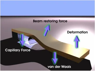
Motivation
Several unresolved problems remain a challenge to continuing the development of
molecular electronics, as outlined above. In particular, this work aims to alleviate the core issues of
1. incomplete understanding of electrical characteristics of a molecular junction 2. lacking strategy for integrating characterization structures into a molecular devices. The first challenge arises primarily due to several key factors
a) lack of control over and sometimes observability of the physical structure of characterization testbeds at the molecular scale
b) effects due to metallic or semimetallic contacts may dominate over effects originating from the sandwiched molecule under investigation
The second challenge arises mostly due to two reasons
a) shortage of testbeds fabricated using standard lithographic techniques amenable to large-scale integration
b) difficulty of translating data obtained in a given experimental testbed setup to a different device structure, which is due to effects introduced by the nature of the contacts
Several lithographically defined test structures have been built using physical vapor deposition onto a self-assembled monolayer of the molecule of interest [Lee1, Zhou1, Chen1, Chen2, Walker1, DeBoer1]. While this technique would allow for the fabrication of integrated devices, it has proven difficult to prevent shorting of the devices due to the impact of high-energy metal particles on a molecular monolayer [Lee2, Kagan1, Li1, Kushmerick4].
[Blum1, Cui1], mechanical break junctions [Reed1, Weber1], liquid metal contacts [Li2, Rampi1], bending wires [Kushmerick1], colloidal trapping, etc.
The aim of this research is to build a testbed that employs lithographically patternable contacts for device integratability, yet avoids the physical-vapor deposition step in favor of a gentler approach for obtaining the second contact.
Figure 3-1: Stiction Test Structure Concept
A useful side-effect of the prefabricated nature of the “stiction” approach is that the molecular self-assembly step is a back-end processing step due to the reversed process order, relieving restrictions normally associated with post-assembly thermal budgets. In the following sections, the details of the necessary processing steps will be described, as well as the characterization of the physical structure and electronic behavior.
Stiction Process
Processing Steps
Table 3-1: Processing steps (traveler) for the stiction structure
Process Traveler: Stiction Testbed - Stepper Step Substep Description
1 Unpack and Scribe Wafers
1.1 Unpack wafers from case and inspect - 4" n++ type - 0.005-0.020 Ohm-cm 1.2 Scribe wafers with unique ID off-angle from major flat
1.3 N2 gun - remove dust
2 JTB-111 Clean
2.1 Clean using JTB-111 solution (prepare fresh if >1 day old) 965ml JTB-111
212ml H2O2
4823ml of DI water 10 minute soak 2.2 N2 gun - blow dry
3 Thermal oxidation of wafers - FOX
3.1 Insert FOX monitor
3.2 Wet oxidation of wafers (1200A) using the std. recipe on the furnace Boat out w/ N2 high
Load wafers
1000C Steam, 2% HCl oxidation N2 Idle: 800sccm, N2 Run: 7200sccm O2 low: 72sccm, O2 high: 1250sccm HCl: 61sccm
3.3 Nanometrics measurement of oxide thickness
4 Metal1 Photolithography
4.1 Solvent clean using DI water rinse
spin wafer and do not let acetone dry before covering in MeOH 4.2 N2 blow dry and Dehydration bake, 5 min 115C
NO HMDS!!!
4.3 Manual dispense and Headway spin of LOR5A spin rate 3000rpm, time 40s, slow start 4.4 10 minute bake at 150C, cool
4.5 Manual dispense and Headway spin of AZ510A PR spin rate 4000rpm, time 40s
4.6 1 minute bake at 90C, cool
4.7 Expose "NanocellStepper_Metal2!!!" mask (DF) using GCA Stepper Exposure: Focus:
4.8 1 minute post-exposure bake at 90C, cool
4.9 Develop wafers using MF319 for 80s (fresh solution in dishes, longer if old) gently swirl solution/rock back-and-forth once every 2 seconds 4.10 9-cycle rinse and N2 dry
5 E-beam evaporation
5.1 Load samples, QCM and Au, Ti targets into E-beam evaporation tool 5.2 Deposit 150A of Ti, then 1400A of Au
use e-beam worksheet
6 Liftoff of Metal1
6.1 Submerge/spray wafers - n-methyl-pyrrolidinone in evaporation dishes - 30 min 6.2 Agitate, move into clean dishes (use filter paper for liftoff waste)
Table 3–1 (continued)
Step Substep Description
7 Contact Photolithography
7.1 Solvent clean using acetone/MeOH rinse
spin wafer and do not let acetone dry before covering in MeOH 7.2 N2 blow dry and Dehydration bake, 5 min 115C
7.3 Manual dispense and Headway spin of HMDS spin rate 4000rpm, time 40s
7.4 Manual dispense and Headway spin of AZ510A PR spin rate 4000rpm, time 40s
7.5 1 minute bake at 115C, cool
7.6 Expose "Nanocell_StepperContact" mask (DF) using GCA Stepper Align to Metal2 mask
Exposure: Focus: 7.7 1 minute post-exposure bake at 90C, cool 7.8 Develop wafers using MF319 for 45s
gently swirl solution/rock back-and-forth once every 2 seconds 7.9 9-cycle rinse and N2 dry
8 Hardbake
8.1 5 minute bake at 115C, cool
9 Dice into samples
9.1 Dice into individual samples prior to release
10 BOE Etch
10.1 Etch samples into BOE using teflon (evaporation) dishes, 30-40 min ~every minute, agitate and release shard if stuck to dish floor 10.2 Transfer to DI dish
Use fluid transfer technique with spoon to keep wet during transfer Thoroughly swirl sample in bath
11 Strip Photoresist
11.1 Transfer to n-methyl-pyrrolidinone dish
Use fluid transfer technique with spoon to keep wet during transfer Gently swirl sample, 5 min strip
11.2 Transfer to DI dish
Use fluid transfer technique with spoon to keep wet during transfer Thoroughly swirl sample in bath
12 Self-Assembly
12.1 Transfer to EtOH dish
Use fluid transfer technique with spoon to keep wet during transfer Thoroughly swirl sample in bath
12.2 Prepare molecular solution of approximately 1-10mM concentration Best if existing solution is diluted in EtOH - avoid precipitation 12.3 Transfer to self-assembly dish
Use fluid transfer technique with spoon to keep wet during transfer 12.4 SAM formation
Soak in molecular solution for appropriate time (24 h) 12.5 Rinse sample in EtOH (2x)
Use fluid transfer technique with spoon to keep wet during transfer Thoroughly swirl sample in dish - remove remaining thiols
13 Rinse and Dry
13.3 Transfer to DI dish - only keep immersed for seconds
Use fluid transfer technique with spoon to keep wet during transfer Immediately dry after a short(!!!) rinse (30s or less)
C
HOICE OFS
UBSTRATEFirst, a highly doped substrate (n++ Si) was chosen to minimize the Schottky effect at the metal-substrate junction. The substrates are specified as 0.001-0.005Ω-cm resistivity, As-doped. Four point probe measurement results on sample wafers showed resistivities of 0.008-0.012Ω-cm, corresponding to 1-5*1018cm-3 doping concentration [Sze1].
T
HERMALO
XIDATIONThe substrates were oxidized 1200A in a wet thermal oxidation process at 1050°C with 4% HCl to minimize defects and ions in the oxide.
F
IRST-
LEVELP
HOTO(L
IFTOFFS
TACK)
A LOR5A liftoff photoresist manufactured by MicroChem was then spun on. We avoided using HMDS adhesion promoter to prevent modifying the SiO2 surface in unforeseeable
E
LECTRON-
BEAMM
ETALE
VAPORATIONThrough electron beam deposition, a 100 Å thick layer of Ti and then a 1500 Å thick layer of Au were put down, and patterned via liftoff to produce the cantilever and pad structures, with minimum feature sizes of 1 micron. The Ti layer is put down at a very slow rate (0.1-0.3Å/s), as are the initial 100Å of Au to give a good quality film. Ti was chosen as the adhesion layer for its extremely fast etch rate in hydrofluoric based etchants (roughly 100 times faster than SiO2) [Williams1], thus by utilizing the Ti underlayer, a much quicker
lateral undercut rate can be achieved in the subsequent release step, as the Ti is etched out much quicker under the cantilever than just SiO2 would be.
L
IFTOFFThe metal patterning is performed by dissolution of the photoresist stack in either
S
ECOND-
LEVELP
HOTOAfter the liftoff, a second level photostep is performed, so that the photoresist protects the structures everywhere except where the cantilever that is to be undercut. The PR used here was a single layer of AZ 510A photoresist, which is subsequently hardbaked at 115°C for 5 to 6 minutes.

![Figure 2-3: Energy level diagram and band lineup of benzene-1,4-dithiol on Au. Reprinted from [Xue1]](https://thumb-us.123doks.com/thumbv2/123dok_us/1588964.1195845/27.612.178.459.138.509/figure-energy-level-diagram-lineup-benzene-dithiol-reprinted.webp)
![Figure 2-4: Electrostatic potential distribution in a molecular junction. Reprinted from [Tian1]](https://thumb-us.123doks.com/thumbv2/123dok_us/1588964.1195845/28.612.100.528.73.294/figure-electrostatic-potential-distribution-molecular-junction-reprinted-tian.webp)