ABSTRACT
BISHOP, SEANN MICHAEL GERWITZ. Polytype Stability, Microstructural Evolution, and Impurities at the Interface of Homoepitaxial 4H-SiC(1120) Thin Films Grown via Hot-Wall Chemical Vapor Deposition. (Under the direction of Dr. Robert Davis).
The electronic properties of 4H-SiC make it a leading semiconductor material for high-power applications. Despite advances in SiC crystal growth, devices fabricated in 4H-SiC(0001) continue to be limited by defects like micropipes, dislocations and stacking faults. Investigations performed here on non-basal SiC have demonstrated micropipe-free, 4H-SiC(1120) films comparable with conventional 4H-SiC(0001). Improved device performance has been achieved for p-i-n rectifiers fabricated in 4H-SiC(1120).
POLYTYPE STABILITY, MICROSTRUCTURAL
EVOLUTION, AND IMPURITIIES AT THE INTERFACE
OF HOMOEPITAXIAL 4H-SiC(
11
2
0
) THIN FILMS GROWN
VIA HOT-WALL CHEMICAL VAPOR DEPOSITION
By
SEANN M. G. BISHOP
A dissertation submitted to the Graduate Faculty of North Carolina State University
in partial fulfillment of the requirements for the Degree of
Doctor of Philosophy
MATERIALS SCIENCE AND ENGINEERING
Raleigh, NC
2006
APPROVED BY:
Dr. Robert F. Davis Dr. C. Lewis Reynolds, Jr. Chair of Advisory Committee
BIOGRAPHY
ACKNOWLEDGEMENTS
TABLE OF CONTENTS
LIST OF TABLES... viii
LIST OF FIGURES ... x
1. Introduction... 1
1.1 Brief History ... 2
1.2 SiC Crystallography and Polytypism... 2
1.3 Theories of Polytypism in SiC... 3
1.4 Properties of SiC ... 4
1.5 SiC Crystal Growth – Chemical Vapor Deposition... 6
1.5.1 Cold Wall Chemical Vapor Deposition ... 7
1.5.2 Hot Wall Chemical Vapor Deposition... 7
1.5.3 High Temperature Chemical Vapor Deposition ... 8
1.5.4 Commercial SiC Chemical Vapor Deposition Systems... 9
1.6 Defects in SiC – Stacking Faults ... 10
1.6.1 Perfect Dislocation Dissociation... 10
1.6.2 Partial Dislocation Characteristics... 11
1.6.3 Classification and Formation of Stacking Faults in 4H-SiC... 11
1.6.4 Stacking Fault Development in 4H-SiC ... 12
1.6.5 Stacking Fault Formation and Growth in 4H-SiC p-i-n Devices. 13 1.6.5.1 Stacking Fault Formation... 14
1.6.5.2 Stacking Faults – Electrically Active Defects ... 15
1.6.5.3 Stacking Fault Growth and the Driving Force... 15
1.7 Dissertation Overview ... 16
1.8 References... 17
1.9 Tables... 25
1.10 Figures... 26
2. Sublimation Growth of an In-Situ Deposited Buffer Layer in SiC Chemical Vapor Deposition on 4H-SiC(1120) Substrates... 34
2.1 Abstract... 35
2.2 Introduction... 36
2.3 Experimental Procedure... 39
2.4 Results and Discussion ... 40
2.4.1 Identification and Growth of In-Situ Deposited SiC... 40
2.4.2 Kinetic Factors in SiC Epitaxial Growth ... 42
2.4.2.1 Epitaxial Growth without Precursors (PR2) ... 42
2.4.2.2 Epitaxial Growth with Precursors (PR1) ... 44
2.4.3 Microstructural Characterization of In-Situ Deposited SiC... 46
2.5 Conclusions... 48
2.6 Acknowledgements... 48
2.7 References... 49
3. Epitaxial Growth of 4H-(1120) and 6H-(0001) SiC: the Role of an In-Situ
Deposited Buffer Layer ... 63
3.1 Abstract... 64
3.2 Introduction... 65
3.3 Experimental Procedure... 66
3.4 Results... 67
3.4.1 In-Situ Layer Identification... 67
3.4.2 Polytype Distribution... 68
3.4.3 Surface Microstructure... 70
3.4.4 Defect Microstructure ... 70
3.5 Discussion... 71
3.6 Summary ... 73
3.7 Acknowledgements... 74
3.8 References... 75
3.9 Tables... 78
3.10 Figures... 79
4. On the Origin of Aluminum-Related Emissions and Impurities at the Interface of Sublimation Grown 4H-SiC(1120) Thin Films ... 88
4.1 Abstract... 89
4.2 Introduction... 90
4.3 Experimental Procedure... 91
4.4 Results and Discussion ... 92
4.4.1 Evolution of Cathodoluminescence Emissions... 92
4.4.2 Model for Site-Competition in SiC Sublimation Growth... 95
4.4.2.1 SiC Decomposition ... 96
4.4.2.2 Film Thickness: Temperature-Dependence ... 97
4.4.2.3 Aluminum Concentration: Temperature-Dependence.. 99
4.4.2.4 Correlation and Significance... 100
4.5 Summary and Conclusions ... 102
4.6 Acknowledgements... 102
4.7 References... 103
4.8 Figures... 106
5. Low Temperature Homoepitaxial Growth of 4H-SiC(1120) Thin Films: Microstructural Evolution and Interfacial Impurity Reduction... 113
5.1 Abstract... 114
5.2 Introduction... 115
5.3 Experimental Procedure... 117
5.4 Results and Discussion ... 119
5.4.1 Heating Prior to Epitaxial Growth ... 119
5.4.2.1 H2 Atmosphere (HC1)... 124
5.4.2.2 Ar Atmosphere (HC2)... 126
5.4.2.3 H2/C2H4 Atmosphere (HC3) ... 128
5.4.2.4 Site-Competition and Impurity Sources... 129
5.5 Supplemental Discussion – Microstructural Evolution ... 130
5.5.1 Sublimation Growth Regime ... 131
5.5.2 Precursor Growth Regime... 133
5.6 Summary ... 135
5.7 Acknowledgements... 136
5.8 References... 137
5.9 Tables... 140
5.10 Figures... 142
6. Polytype Stability and Microstructural Characterization of SiC Epitaxial Films Grown on [1120]- and [0001]-Oriented SiC Substrates... 163
6.1 Abstract... 164
6.2 Introduction... 165
6.3 Experimental Procedure... 166
6.4 Results... 168
6.4.1 Polytype Analysis ... 168
6.4.2 Surface Microstructure... 173
6.4.3 Defect Microstructure ... 176
6.5 Conclusions... 178
6.6 Acknowledgements... 179
6.7 References... 180
6.8 Tables... 184
6.9 Figures... 186
7. Characterization and Comparison of 4H-SiC(1120) and 4H-SiC(0001) 8° Off-Axis Substrates and Homoepitaxial Films... 195
7.1 Abstract... 196
7.2 Introduction... 197
7.3 Experimental Procedure... 197
7.4 Results and Discussion ... 199
7.5 Summary ... 201
7.6 Acknowledgements... 201
7.7 References... 202
7.8 Tables... 203
7.9 Figures... 204
8. Summary... 209
A1. Growth Evolution and Pendeo-Epitaxy of Non-Polar AlN and GaN Thin
Films on 4H-SiC(1120) ... 214
A1.1 Abstract... 215
A1.2 Introduction... 216
A1.3 Experimental Procedure... 216
A1.4 Results and Discussion ... 217
A1.5 Summary ... 221
A1.6 Acknowledgements... 222
A1.7 References... 223
A1.8 Figures... 224
A2. Example Calculations for Site-Competition Model ... 229
A3. Chemical Vapor Deposition System Design and Description ... 236
A3.1 Abstract and Introduction ... 237
A3.2 Gas Temperature and Flow Modeling ... 237
A3.3 Induction Heating Considerations... 240
A3.4 Final System Design and Layout ... 242
A3.5 References... 246
A3.6 Tables... 247
LIST OF TABLES
CHAPTER 1
1. Crystallographic information for basic SiC polytypes. ... 25
2. Electronic properties of SiC and other conventional semiconductors materials. 25 3. Stacking sequences for intrinsic and extrinsic Frank faults in 4H-SiC ... 25
CHAPTER 2 1. Comparison of the atomic concentration of nitrogen and aluminum impurities within epitaxial layers on 4H-SiC(1120) substrates... 52
CHAPTER 3 1. Comparison of atomic concentrations of N and Al impurities within epitaxial layers on 4H-SiC(1120) and 6H-SiC(0001) substrates... 78
2. Mode designations and positions of Raman peaks for homoepitaxial layers grown on 4H-SiC(1120) substrates... 78
3. Summary of the cathodoluminescence spectrum from homoepitaxial layers grown on 4H-SiC(1120) substrates at 6K. ... 78
4. Dimensions of surface feature for epitaxial layers grown on 6H-SiC(0001) substrates... 78
CHAPTER 5 1. Important process conditions used during heating experiments. ... 140
2. Important process conditions used during epitaxial growth experiments... 140
3. Surface feature dimensions after heating in a hydrogen diluent (HC1)... 140
4. Surface feature dimensions after heating in an argon diluent (HC2)... 140
5. Surface feature dimensions after heating in a hydrogen diluent (HC1) and subsequent epitaxial growth... 141
CHAPTER 6 1. Values of measured and calculated peak separation of symmetric reflections for epitaxial films on 4H- and 6H-SiC substrates... 184
2. Values of measured and calculated peak separation of asymmetric reflections for epitaxial films on 4H- and 6H-SiC substrates... 184
3. Summary of the cathodoluminescence spectra from epitaxial films on 4H-SiC(1120) and 6H-SiC(0001) substrates at 300 K... 184
4. Mode designation and position of the Raman peaks for epitaxial films on 4H-SiC(1120) substrates. ... 185
5. AFM surface roughness comparison for epitaxial films on 4H- and 6H-SiC . substrates... 185
CHAPTER 7
1. Layer thicknesses and doping concentrations in the p-i-n device structures. ... 203
2. Average blocking voltage and forward voltage drop at 100 A/cm2 for 4H-SiC(1120) and 4H-SiC(0001) p-i-n devices of varying size... 203
APPENDIX 3 1. Summary of the variables employed in the experimental matrix ... 247
2. Summary of the results obtained from the simulations ... 247
3. Purification information for porous graphite insulation employed in this research ... 248
4. Purification information for the dense graphite employed in this research. ... 249
5. Important vendor information, dimensions, and quantities for the graphite that comprise the reaction chamber. ... 250
6. Properties of the porous and dense graphite used in this research... 251
7. Seal type(s) for the major vacuum system components... 252
LIST OF FIGURES
CHAPTER 1
1. (a) Representation of atoms in “A-sites” (black circles) on close-packed planes. Equivalent close-packed planes with atoms in “B-sites” (diamonds) or “C-sites” (black squares) can occur above or below the plane in (a). Unit cells for 3C-, 4H, and 6H-SiC are shown in (b). (c) Schematic of the binary tetrahedral structure of SiC. Silicon and carbon atoms are represented by light and dark spheres, respectively ... 26
2. SiC polytype stability diagrams. ... 27
3. Plot of forward voltage (Vf) versus the blocking voltage for 4H-SiC and Si p-i-n devices (solid line). The Vf (at high blocking voltage) for SiC devices is lower than the extrapolated values for Si devices (dotted line).. 28
4. Illustrations of the growth chambers for (a) horizontal, CW-CVD,
HW-CVD ((b) horizontal and (c) vertical), and HT-HW-CVD... 29
5. (a) Stacking fault created by perfect dislocation (b1) dissociation into partial dislocations (b2 and b3) in the face-center cubic lattice. (b) Perfect (b1) and partial dislocations (b2 and b3) in a close-packed arrangement, showing two pathways that result in the same shear displacement ... 30
6. Formation of single (b) and double (c) Shockley faults from perfect
4H-SiC (a) ... 31
7. (a) The separation between the solid and dotted lines illustrates the drift in the forward voltage that occurs in 4H-SiC(0001) p-i-n devices after long-term forward operation. (b) Cathodoluminescence image (left) and x-ray topograph (right) of stacking faults formed in 4H-SiC(0001) p-i-n
device ... 32
CHAPTER 2
1. Schematic of the radiantly heated, vertical hot-wall chemical vapor deposition system used for SiC epitaxy growth. All of the dense graphite
parts are coated with SiC... 53
2. Temperature-time diagrams that illustrate the two process routes (PR) used for homoepitaxial growth of SiC films. In PR1 (a), SiH4 and C2H4 were admitted at the growth temperature. No precursors gases were used during PR2 (b). Hydrogen was the diluent gas during all steps of (a). For (b) hydrogen or argon were employed as the diluent gas... 54
3. Thickness as a function of growth time at 1450ºC for epitaxial growth using PR1 and holders A and C. The growth rate (slope) was 509 nm/hr and the in-situ layer thickness (intercept) was 108 nm for holders A and C, independent of the hydrogen flow rate. The flow rate of the hydrogen diluent was 590 sccm for holder A; 590 and 1000 sccm of hydrogen were used for holder C. The C/Si ratio was held constant at 1.00... 55
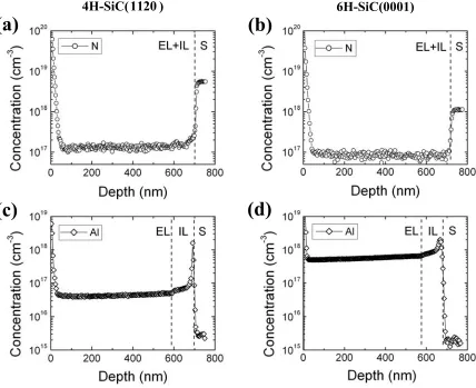
4. SIMS concentration depth profiles for (a) nitrogen and (b) aluminum in the epitaxial layer (EL), the in-situ deposited buffer layer (IL), and the 4H(1120) substrate (S) after epitaxial growth using PR1 and holder C at 1450ºC. The hydrogen flow rate was 1 slm, and the C/Si ratio was 0.35.. 56
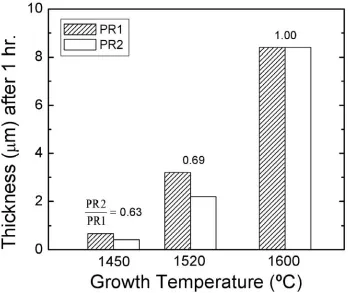
5. Bar graph of the thickness after 1 hour of growth using PR1, PR2 and holder A between 1450-1600ºC. The ratio of the thicknesses from latter and former routes (PR2/PR1) increased from 0.63 to 1.00 over this temperature range. The hydrogen flow rate was 0.59 slm, the C/Si ratio was 1.00... 57
6. Arrhenius plots for epitaxial layers grown using PR2 and holder C compared with literature. The hydrogen and argon flow rate was 1.00 slm ... 58
7. Arrhenius plot for epitaxial layers grown using PR1 and holder C. The hydrogen flow rate was 1.00 slm and the C/Si ratio was 1.00. ... 59
9. (a) Cross-sectional TEM image of a ~1 µm epitaxial layer grown using PR2 and holder C on a 4H(1120) substrate at 1450ºC. (b) Higher magnification image of the same sample as (a). Images (a) and (b) were acquired along the [01 ] zone axis and the [0001] zone axis, 10 respectively. The white diagonal feature in each image is the glue line. The hydrogen flow rate was 1.00 slm and the C/Si ratio was 1.00... 61
10. Cross-sectional TEM image of a ~1 µm epitaxial layer and a ~100 nm in-situ deposited buffer layer after epitaxial growth on a 4H(1120) substrate at 1450ºC using PR1 and holder C. The image was acquired along the [0001] zone axis; the black diagonal feature is the glue line. The hydrogen flow rate was 1.00 slm and the C/Si ratio was 1.00 ... 62
CHAPTER 3
1. SIMS concentration-depth profiles for nitrogen (N) and aluminum (Al) within the epitaxial layers on ((a) and (c)) 4H-SiC(1120) and ((b) and (d)) 6H-SiC(0001) substrates (S). The layer grown via the PG route and the in-situ deposited layer are denoted as EL and IL, respectively. The hydrogen flow rate was 1 slm and the C/Si ratio was 1.00 ... 79
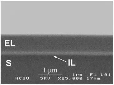
2. Cross-sectional SEM micrograph of the epitaxial layer (EL), in-situ deposited layer (IL), and 6H-SiC(0001) substrate (S). The flow rate of the diluent hydrogen was 1 slm and the C/Si ratio was 0.35 ... 80
3. HRTXD ω-2θ scans of symmetric reflections for epitaxial layers grown via the SG route on (a) 6H-SiC(0001) and (b) 4H-SiC(1120) substrates .. 81
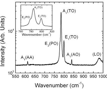
4. Raman spectrum from 550-1000 cm-1 of a 1 µm thick epitaxial layer from SG on a 4H-SiC(1120) substrate. Inset is a high-resolution Raman spectrum from 760-820 cm-1... 82
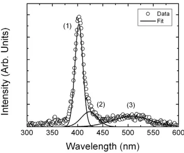
5. Cathodoluminesence spectrum obtained at 6 K for a 1 um thick epitaxial layer grown via the SG route on a 4H-SiC(1120) substrate... 83
6. Plan-view TEM electron diffraction pattern obtained from an epitaxial layer grown via the SG route on a 4H-SiC(1120) substrate along the [1120] zone-axis. The numbered diffraction spots indicate (1) = [0004], (2) = [01 ], and (3) = [12 01 ]...10 84
8. 10 x 10 µm AFM height images of the epitaxial surface of a ~100 nm thick in-situ layer on (a) 4H-SiC(1120) and (b) 6H-SiC(0001) substrates after heating to the growth temperature in 1 slm H2. The RMS roughness values for (a) and (b) are 0.31 nm and 3.65 nm, respectively... 86
9. (a) Optical micrograph of the surface of a 1 µm thick 4H(1120) layer deposited via SG after etching at 700ºC for one minute. (b) Cross-sectional TEM image of a similarly deposited epitaxial layer on a 4H-SiC(1120) substrate. The zone axis is [01 ]. The white diagonal 10 feature is the glue line. The area that contains the film-substrate interface (not distinguishable) is located in the upper right corner of the figure ... 87
CHAPTER 4
1. Plot of the interaction volume as a function of electron beam energy. Simulation conditions are summarized by N/R. N refers to the number of electrons and R is the radius of the electron beam ... 106
2. Cathodoluminescence spectrum of an as-received 4H-SiC(1120) substrate obtained at 25 keV and 300 K. N-DV is the nitrogen
donor-to-valence band transition... 107
3. Cathodoluminescence spectra for a 1 µm epitaxial layer on a 4H-SiC(1120) substrate obtained 300 K and (a) 10 keV, (b) 15 keV, and (c) 25 keV. N-DV is the nitrogen donor-to-valence band transition. NAl-DAP refer to the nitrogen-to-aluminum and nitrogen-to-boron donor-to-acceptor pair (DAP) transitions, respectively. The conduction band-to-aluminum acceptor level transition is Al-CA, and Int. Ox. is an abbreviation for interface oxygen-related emission... 109
4. Cathodoluminescence spectrum for a 1 µm epitaxial layer on a 4H-SiC(1120) substrate obtained 6 K and 25 keV. N-DV is the nitrogen donor-to-valence band transition, and the conduction band-to-aluminum acceptor level transition is Al-CA. NAl-DAP and NB-DAP refer to the nitrogen-to-aluminum and nitrogen-to-boron donor-to-acceptor pair (DAP) transitions, respectively ... 110
6. Aluminum concentration as a function of film thickness from Fig. 5(b) (cirlces) and calculated based on Eqs. 8 and 12 (line). The calculations are shown in the appendix. 0 nm signifies the film-substrate interface located at ~530 nm in Fig. 5(b)... 112
CHAPTER 5
1. 5 .00 x 5.00 µm AFM images of the (1120) surface microstructure after heating in hydrogen (HC1) to (a) 1250°C, (b) 1350°C, and (c) 1450°C. Higher resolution 0.75 x 0.75 µm AFM images are shown in (d)-(f). The
vertical scale is given in the upper right corner of each image... 142
2. (a) The RMS surface roughness and (b) the step height and terrace width plotted as a function of temperature for HC1 (open circles) and HC2 (dark squares). The RMS values in (a) are based on the 5.00 x 5.00 µm AFM images in Fig. 1 (HC1) and Fig. 4 (HC2)... 143
3. Line scans showings the presence of a step-and-terrace microstructure on the (1120) surface after heating to 1250ºC in (a) hydrogen (HC1) and (b) argon (HC2). The line scans were extracted from Fig. 1(d) and Fig. 4(d), respectively. The black arrows indicate steps ... 144
4. 5 .00 x 5.00 µm AFM images of the (1120) surface after heating in argon (HC2) to (a) 1250°C, (b) 1350°C, and (c) 1450°C. Higher resolution 0.75 x 0.75 µm AFM images are shown in (d)-(f). The vertical scale is given in the upper right corner of each image. The white arrows in (a) indicate surface undulations reminiscent of polishing scratches ... 145
5. SIMS concentration-depth profiles for (a) aluminum and (b) nitrogen after HC2. The temperatures are indicated in the upper right corner of each image; the dwell time was 60 minutes... 146
6. 2.50 x 2.50 µm AFM height images of the (1120) surface microstructure after heating from (a) 1200-1450ºC and (b) 1400-1450ºC in an C2H4 overpressure of 1.15x10⁻² Torr (HC3). The corresponding phase images are shown in (c) and (d), respectively. The RMS roughness is plotted as a function of dwell time at 1450°C in (e). The dwell time for (a)-(d) was 0 minutes ... 147
8. SIMS concentration-depth profiles of aluminum impurities within epitaxial layers grown at 1250°C (squares) and 1350°C (circles). Hydrogen was the diluent gas during heating (HC1), growth and cooling.... 149
9. 5.00 x 5.00 µm AFM height images of the (1120) surface microstructure after heating in hydrogen (HC1) and epitaxial growth at (a) 1250°C and (b) 1350°C. The RMS roughness and terrace width are plotted versus temperature in (c). The RMS values in (c) were determined from 5.00 x 5.00 µm AFM images. (d) 2.50 x 2.50 µm image of the surface in (a). Growth pits are marked by white arrows in (a) and (d) ... 150
10. 1.50 x 1.50 µm AFM height images showing the microstructural evolution of (1120) SiC after (a) heating to 1450°C in hydrogen (HC1) and (b)-(f) subsequent epitaxial growth from SiH4 and C2H4. The layer thickness is shown in the lower left corner of each image. The black arrows indicate the [0001] and [ 0011 ] crystallographic directions... 151
11. RMS roughness of SiC layers of different thickness epitaxially grown at 1450°C. Heating was performed in hydrogen (HC1) prior to film deposition from SiH4 and C2H4. The RMS values were determined from the 1.50 x 1.50 µm AFM images shown in Fig. 10... 152
12. SIMS concentration-depth profile of aluminum following epitaxial growth at 1350°C. Argon was the diluent gas during heating (HC2). Prior to precursor injection, growth was suspended 5 minutes after switching to a hydrogen diluent; the latter resulted in the decomposition and re-deposition of the SiC coating and an increase in the aluminum impurities in the region labeled IL (in-situlayer). Epitaxial layer refers to f SiH4 and C2H4 ... 153
13. 1.50 x 1.50 µm AFM height images showing the microstructural evolution of (1120) SiC after (a) heating to 1350°C in argon (HC2), a (b) 1 minute and (c) 5 minute exposure to hydrogen, and (d)-(f) subsequent epitaxial growth from SiH4 and C2H4. The layer thickness is shown each image. The black arrows indicate the [0001]- and [ 0011 ]-direction... 154
15. 1.50 x 1.50 µm AFM height images showing the microstructural evolution of (1120) SiC after (a) heating to 1250°C in argon (HC2), a (b) 5 minute exposure to hydrogen, and (c) subsequent epitaxial growth from SiH4 and C2H4. The layer thickness is shown in the lower left corner of each image. The black arrows indicate the [0001] and [ 0011 ] crystallographic directions ... 156
16. 10 x 10 µm AFM height images of the (1120) surface microstructure following epitaxial growth at 1450°C. Heating was performed from (a) 1200-1450ºC and (b) 1400-1450ºC in an C2H4 overpressure of 1.15x10⁻² Torr (HC3). The dwell time at 1450°C was 0 minutes for (a) and (b) prior to precursor injection. The dark circle in (a) is a growth pit ... 157
17. SIMS concentration-depth profile of aluminum impurities near the film- substrate interface, following epitaxial growth at 1450°C. Heating was performed from 1200-1450ºC in an C2H4 overpressure of 1.15x10⁻² Torr (HC3). The dwell time at 1450°C was 0 minutes prior to precursor injection... 158
18. Plot of the ionized donor concentration (ND-NA) and the difference in the atomic concentration ([N]-[Al]) as a function of the C/Si ratio. The ND-NA values were determined by CV measurements and the atomic concentration of nitrogen [N] and [Al] were determined by SIMS. The C/Si was changed by varying the flow rate of SiH4 from 1.20-3.43 sccm. The C2H4 was held constant at 0.60 sccm... 159
19. SIMS concentration-depth profiles of nitrogen, aluminum, and boron impurities within the protective SiC coating on the graphite parts used in
this research... 160
20. (a) Schematic illustration of the surface diffusion model. (b) Temperature dependence of the surface diffusion length on the (0001)Si and (0001)C surfaces of 6H-SiC... 161
21. a) 5.00 x 5.00 µm and (b) 0.75 x 0.75 µm AFM images of the (1120) surface after heating in argon (HC2) to 1450°C. The dwell time for (a) and (b) was 60 minutes ... 162
CHAPTER 6
2. Cathodoluminesence spectra at 300 K for 1 um thick epitaxial layers on (a) 6H(0001) on-axis and (b) 4H(1120) substrates ... 187
3. Raman spectra of (a) the reference 4H(1120) substrate and (b) a 1 µm
epitaxial layer on a 4H(1120) substrate... 188
4. High-resolution Raman spectra of (a) the reference 4H(1120) substrate and (b) a 1 µm epitaxial layer on a 4H(1120) substrate ... 189
5. (a) Cross-sectional and (b) plan-view TEM electron diffraction patterns obtained from an epitaxial layer on a 4H(1120) substrate along the [01 ] zone-axis and [10 1120] zone-axis, respectively. The diffraction spot: (1) = [0004], (2) = [11 ], (3) = [24 1120], (4) = [0004], (5) = [01 ], 12
and (6) = [01 ]. ...10 190
6. Optical (NDIC) micrographs of the epitaxial surface of layers on (a) 4H(1120), (b) 4H(0001) on-axis, and (c) 4H(0001) 8º off-axis. The surface of an epitaxial layer on a 6H(0001) on-axis substrate is shown in the SEM image marked (d) ... 191
7. 5 µm x 5 µm AFM height images of the epitaxial surface of layers on (a) 4H(1120), (b) 4H(0001) on-axis, (c) 4H(0001) 8º off-axis, and (d) 6H(0001) on-axis substrates. The vertical scale for (a)-(d) is 1.35 nm, 1.18 nm, 19.30 nm, and 2.54 nm, respectively. The inset in (a) is 500 nm x 500 nm and the vertical scale is 0.40 nm. 1 and 2 denote a specular area and region with macrosteps in (c), respectively. The insets in (c) and (d) are line scans that detail the change in surface topography as a result of step bunching ... 192
8. Optical (NDIC) micrographs (etch time) of (a) an as-received 4H(1120) substrate (5 min.), (b) a 1 µm epitaxial layer (1 min.), and (c) a 2.5 µm epitaxial layer (1 min.) after defect etching in molten KOH at 700ºC... 193
CHAPTER 7
1. Maps of the full-width half-maxima (FWHM) of the XRC for a 4H(1120) and 4H(0001) 8º off-axis substrate and films epitaxial grown on the latter substrates. The range in FWHM for the 4H(1120) and 4H(0001) 8º off-axis substrate is 0-140 and 0-224, respectively. The range in FWHM for the epitaxial layers on these substrates is 0-141 and 0-246 ... 204
2. Nomarski interference optical micrograph of a defect on the surface of a 4H(1120) epitaxial layer. The dark line ending in the middle of the image is a micropipe intersecting the epitaxial layer-substrate interface at a shallow angle. The micropipe does not penetrate through the interface; the origin of the surface defect is likely related to the micropipe... 205
3. Cross-sectional, bright field TEM (0110) micrograph of the film-substrate interface (indicated by white arrows), with associated diffraction pattern. Partial dislocations most likely bounding stacking faul vertically, but appear with alternating light and dark contrast, indicating inclination to the image plane. The stacking faults penetrate into the substrate ... 206
4. Hall mobility versus temperature in an n-type [1120]-oriented 4H-SiC film grown in this research and in similar [0001]-oriented films grown by other investigators ... 207
5. LTPL spectrum for a [1120]-oriented film showing an FE and N-BE emission line (bottom) as compared to an undoped [0001]-oriented sample with a sharp FE line (middle) and an n-doped [0001]-oriented sample with sharp N-BE line emission and a suppressed FE line (top)... 208
APPENDIX 1
2. 1.75 x 1.75 µm AFM height images of (a) 10 nm, (b) 25 nm and (c) 50 nm thick AlN (1120) grown on 4H-SiC (1120); the inset in (a) is 0.5 x 0.5
µm. (d) Plots of the root mean square (RMS) (squares) and peak-to-valley (PV) surface roughness (circles) of AlN layers of different thicknesses. The RMS and PV roughness values are average values determined from multiple 2.5 x 2.5 µm AFM images obtained at each thickness ... 225
3. 2 x 2 µm AFM height images of (a) surface of a 100 nm thick AlN(1120) buffer layer and (b) 2 nm and (c) 5 nm thick GaN (1120) films. The inset in (b) is 0.5 x 0.5 µm. (d) Plots of the intensity of the Al2p spectra acquired as a function of the thickness of the overgrown GaN films. (e) Plots of the normalized integrated intensity (IS/I0) for the Al2p peaks shown in (d) for the 2, 5 and 10 nm thick GaN films (squares) and the theoretical curves for the attenuation of the Al2p peaks for VW, SK, and FM growth modes (solid lines) as a function of the thickness of the overlying GaN films. The escape depth, transition thickness, and surface coverage were taken as 1.1 nm, 1.3 nm, and 0.5, respectively ... 226
4. 2 x 2 µm AFM height images of (a) 10 nm, (b) 50 nm, (c) 100 nm, and (d) 1000 nm thick GaN (1120) grown on 100 nm thick AlN (1120) buffer layers. (e) Plots of the root mean square (RMS) (squares) and peak-to-valley (PV) surface roughness (circles) of GaN layers of different thicknesses. The RMS and PV roughness values are average values determined from multiple 5 x 5 µm AFM images obtained at each thickness. Areas I, II, and III indicate stages of microstructural development that occurred during the growth of 2 to 1000 nm thick GaN (1120) films ... 227
5. (a) Cross-sectional and (b) plan-view TEM micrographs of the seed and coalesced “wing” regions, respectively, of PE-GaN (1120) films achieved using a single-step growth process, where T = 1020ºC and the V/III = 660 for 6 hrs. ... 228
APPENDIX 2
1. Temperature-time profile typical for the heating stage of the growth process for a growth temperature of ~1450ºC ... 232
4. Shows the aluminum concentration plotted as a function of the growth temperature, based on Eq. A4 ... 235
APPENDIX 3
1. Modeling results comparing the influence of mass flow rate and total reactor pressure on the temperature distribution and flow pattern in the hot zone. The left side of each image shows the temperature distribution and the right side shows the flow pattern. A color code relating the thermal profile lines and temperature in Kelvin is located at the left of each image. The color of the flow pattern (right side) is not an indicator of temperature or temperature distribution ... 254
2. Modeling results comparing the influence of mass flow rate and total reactor pressure on the temperature distribution and flow pattern in the hot zone. The left side of each image shows the temperature distribution and the right side shows the flow pattern. A color code relating the thermal profile lines and temperature in Kelvin is located at the left of each image. The color of the flow pattern (right side) is not an indicator of temperature or temperature distribution ... 255
3. Modeling results comparing the influence of the gas inlet diameter and the reactor length on the temperature distribution and flow pattern in the hot zone. The left side of each image shows the temperature distribution and the right side shows the flow pattern. A color code relating the thermal profile lines and temperature in Kelvin is located at the left of each image. The color of the flow pattern (right side) is not an indicator of temperature or temperature distribution or temperature distribution... 256
4. Modeling results comparing the influence of the gas inlet diameter and reactor inner diameter on the temperature distribution and flow pattern in the hot zone. The left side of each image shows the temperature distribution and the right side shows the flow pattern. A color code relating the thermal profile lines and temperature in Kelvin is located at the left of each image. The color of the flow pattern (right side) is not an indicator of temperature or temperature distribution ... 257
6. Schematic illustrating the “skin effect” in induction heating. δ is the skin depth referred to as s in the text ... 259
7. Final system design of the hot zone and base assembly ... 260
8. Schematic showing the vacuum and high vacuum assemblies and components ... 261
9. Schematic of the water cooled gas inlet... 262
1.1 Brief
History
SiC is an indirect, wide band gap semiconductor of considerable interest for high power, high frequency, and high temperature device applications. Although research in the past 20 to 30 years has led to rapid maturation of SiC, the history of this material predates the twentieth century. Synthetic SiC was first discovered in 1824 by Berzelius [1]. The first viable process to manufacture SiC was realized by Acheson in the late nineteenth century [2], which led to the commercialization of SiC primarily as an abrasive material. In 1905, naturally occurring SiC was first observed by Moissan while investigating meteorites [3]. Lely [4] introduced an alternative, sublimation-based process in 1955 that employed concentric SiC and graphite tubes heated to ~2100°C. Single crystal SiC platelets grew unconstrained from the reaction of Si vapor with the surface of the graphite. Research conducted by Tairov and Tsvetkov to increase the purity and size of SiC crystals led to the development of the modified-Lely technique in 1978 and enabled the growth of single crystal SiC boules [5]. The modified-Lely technique (with minor adaptations) remains the predominant method in which SiC substrates are grown currently [6]. SiC substrates became commercially available in the late 1980s [7]. In the 1990’s, SiC light emitting diodes became commercially available; however, because of the indirect band gap of SiC and the consequent low internal quantum efficiency, they were soon replaced by optoelectronic devices fabricated in direct band gap III-nitride alloys. Silicon carbide and sapphire soon became the substrate materials of choice on which to grow the material structures for the nitride-based devices [8]. Recently, semi-insulating and n- and p-type conducting SiC substrates have become available with diameters to four inches [9], and SiC devices such as Schottky barrier diodes [10] and metal-semiconductor field effect transistors [11] are now commercially available.
1.2 SiC Crystallography and Polytypism
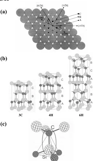
250 polytypes have been reported for SiC [13]. The differences between the polytypes occur in the stacking of the Si/C bilayer sheets along the c-axis. Each bilayer contains one closed-packed layer of Si atoms and one of C atoms. The crystal structures of the SiC polytypes are hexagonal (H), rhombohedral (R), and cubic (C). All of the hexagonal and rhombohedral polytypes are collectively referred to as α-SiC. SiC has only one cubic polytype, which is referred to as β-SiC.
All of the polytypes in SiC can be described by different stacking arrangements of A, B, and C sheets along the <0001>. The A, B, and C designation correspond to atomic positions, as shown in Fig. 1(a). There is one restriction to the stacking order; sheets with the same letter cannot be stacked atop each other.
Due to the large number of polytypes of SiC, different naming schemes have been proposed by Zhadanov [14], Ramsdell [15], and Jagodzinski [16]. The most widely used notation is the Ramsdell notation, where the polytype is designated with a number indicating the stacking direction periodicity and a letter for the unit cell (H, R, or C). Figure 1(b) shows the unit cells for the 3C-, 4H- and 6H-SiC polytypes, and Table 1 lists important crystallographic information for these SiC polytypes.
The basic structural unit of all of the SiC polytypes is the Si- (or C-) tetrahedra, where each silicon atom is surrounded by four carbon atoms (or each carbon atom by four silicon atoms). As a result, SiC has a binary tetrahedral structure, which is shown in Fig. 1(c). The thin lines that form a pyramid at the base of Fig. 1(c) indicate the Si tetrahedra. The silicon atoms outline the corners of the C tetrahedra in the same figure. All tetrahedra (either Si or C) have tetrahedral coordination at each corner. The Si-C bond is 88%-90% covalent and 10-12% ionic [12].
1.3 Theories for Polytypism in SiC
especially when the theory was modified to include growth in faulted structures [20-24] - major obstacles to this theory include: lack of experimental evidence and information regarding the initial dislocation [25]. Other kinetic and growth considerations such as stoichiometry [26-28], impurities [2,29-36], point defects [37-38] and the growth rate [39] have been employed to explain polytype formation in SiC.
Jagodzinski proposed an alternative theory based on thermodynamic considerations [40]. This investigator assumed that the internal energies of the polytypes were similar, 3C was the most stable polytype of SiC, and that all other structures could be derived from stacking fault ordering in this polytype. The driving force for the ordering of stacking faults was claimed to be the contribution of the vibrational entropy to the free energy. Contrary to Jagodzinski’s theory, the cubic polytype was later determined to be a metastable polytype, instead of a stable, low-temperature phase as he originally assumed [41]. Schneer [42] treated polytypism as an order-disorder phenomenon, but no evidence has been reported that correlates a critical temperature with any polytype occurrence in SiC [25]. Fissel has recently used classical nucleation theory to explain SiC hetereopolytypic structures grown by solid-source molecular beam epitaxy [43]. Polytypism has also been studied by energy ab initio calculations based on layer interactions [44-50].
The thermodynamic stability of basic polytypes in SiC has been studied experimentally [2,51] by mapping polytype formation with temperature (Fig. 2). Though no single theory has thus far universally explained polytypism in SiC, general characteristics of the basic polytypes have been determined by experimentation. For example, the 6H polytype is the stable phase at high temperature, while the 4H polytype is more stable at lower temperatures. Because the 2H polytype has the highest formation energy, it is the most difficult polytype to produce. In addition, the 3C polytype is not an equilibrium phase at any temperature.
1.4 Properties of SiC
polytypes, 4H-SiC is currently the leading candidate for next-generation SiC-based devices. The latter is due largely to its high electron mobility. Table 2 compares the principal properties of this SiC polytype to those of Si and GaAs.
The high thermal conductivity and thermal stability of 4H-SiC enable higher temperature device operation than Si. 4H-SiC devices can routinely operate up to ~500°C,
while most Si-based devices are limited to 125°C. Because the thermal conductivity of 4H-SiC is 2-3 times greater than Si, 4H-4H-SiC devices dissipate larger amounts of excess heat while operating at high power [53].
High breakdown electric field strength allows higher voltages to be sustained during operation. When a p-i-n power device is under reverse bias, the maximum blocking voltage, Vmax, can be calculated from the breakdown electric field strength, Emax, by:
2 W E
V max
max = (eq. 1)
where W is the depletion layer width, and a triangular spatial electric field distribution is assumed [54]. Since the 4H-SiC breakdown electric field strength is more than ten times larger than Si, 4H-SiC power devices can maintain operation at significantly higher voltages, as shown in Fig. 3. Figure 3 compares the blocking voltage and forward voltage,Vf, (at 100
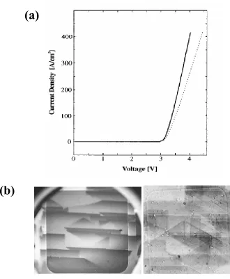
A/cm2) for selected 4H-SiC and commercial Si p-i-n diodes (solid line) [55]. The high breakdown electric field strength of 4H-SiC is the primary reason p-i-n diodes fabricated from this SiC polytype have been demonstrated with the highest blocking voltage (19.5 kV) ever reported for any semiconductor material [55].
1.5 SiC Crystal Growth - Chemical Vapor Deposition
SiC bulk crystals are currently produced by the modified-Lely technique described above. The reader is referred to Ref. [7] and Ref. [56] for an overview of SiC bulk crystal growth and to Refs. [57-59], and the bibliographies therein, for a discussion of recent modifications to this technique that allow better process control and that reduce problems associated with the latter, such as doping, defects and electrical non-uniformities. Growth of single crystal SiC epitaxial layers has been achieved by a variety of growth techniques, namely, molecular beam epitaxy (MBE) [see, e.g., [60-61] and the references therein], liquid phase epitaxy (LPE) [62-63], sublimation epitaxy (SE) [64], and chemical vapor deposition (CVD) (or vapor phase epitaxy (VPE)). While a hallmark of MBE is precise control of the composition and doping concentration [60], the low growth rates that accompany this
1.5.1 Cold Wall Chemical Vapor Deposition
The first microwave power transistor structures [72] and active layers for power rectifiers (i.e. Schottky barrier [73] and p-i-n diodes [74]) were achieved using horizontal, cold wall CVD (CW-CVD) [75]. A schematic of a horizontal, CW-CVD system is shown in Fig. 4(a). Growth rates from 2-6 µm/hr have been reported for this growth technique from 1500-1600°C [77-78]. In 2002, growth rates to 6 µm/hr were reported for “high speed” horizontal, CW-CVD [79]. Thirty micron thick layers were used to produce Schottky diodes with net donor concentrations in the low 1014 cm-3 range. The diodes exhibited a maximum blocking voltage of 3.6 kV [79].
Limitations associated with this technique have been reported. To obtain a 100 µm thick epitaxial layer for a kV-class power device, the growth time could require a period of ~50 hours, based on the growth rates mentioned above. The growth time is ultimately influenced by the lifetime of the SiC coating on the graphite susceptor and other parts because of the extended time needed to grow very thick films [70]. In addition, the thermal gradient, as a result of the cold wall, and the buoyancy-effects in a horizontal reactor can cause non-uniformities in the growth rate, film composition and doping profile [80].
1.5.2 Hot Wall Chemical Vapor Deposition
SiC homoepitaxial growth via horizontal, hot wall CVD (HW-CVD) was introduced in 1994 to obtain high heating and hydrocarbon cracking efficiency [81]. To minimize the radiation losses experienced in horizontal, CW-CVD, insulation was placed around the susceptor [82]. The growth chamber of a horizontal, HW-CVD system is illustrated in Fig. 4(b). Using this growth technique, the first 4.5 kV SiC p-i-n device was produced. The active region thickness and nitrogen doping level were 45 µm and 1x1015 cm-3, respectively [83]. Horizontal HW-CVD has been improved since its original inception [70]. Epitaxial layers have been grown with a thicknesses in excess of 150 µm, at growth rates to 20 µm/hr [85] and with better than 5% thickness uniformity [67].
via metal organic chemical vapor deposition (MOCVD). The advantages of this technique (and chamber orientation) include improved mass transport and uniformity [87]. In addition, the bottom-up gas flow configuration results in high gas velocities [82,88]. A vertical, HW-CVD system is illustrated in Fig. 4(c).
Using vertical HW-CVD, Ellison et al. [68] were able to achieve growth rates ranging from 10-50 µm/hr at 1650-1850°C. SiC epitaxial layers were grown to more than 100 µm with 5% thickness uniformity at growth rates of 20-25 µm/hr. The lowest n-type doping level observed by these authors was 6x1013 cm-3. In addition, Schottky diode structures were processed with 42 µm thick epitaxial layers having an n-type carrier concentration of 5x1014 cm-3. The measured breakdown voltage ranged from 2 to 3.85 kV. Kimoto et al. [69] in 2001 was able to obtain growth rates to 21 µm/hr with 4% and 6% thickness and doping uniformity, respectively, as well as a low n-type background doping concentration of 7.2x1014 cm-3 using a vertical, HW-CVD system. Recently, reproducible growth rates to 60 µm/hr were achieved [89]. The net donor concentration of these films was reported to be nominally 1013 cm-3; the best value obtained was 5x1012 cm-3 for a 75 µm epitaxial layer
grown at 1700°C [89].
1.5.3 High Temperature Chemical Vapor Deposition
High temperature chemical vapor deposition (HT-CVD) is another growth technique developed to improve growth rates and is illustrated in Fig. 4(d). The main distinction between vertical, HW-CVD and HT-CVD is the operating temperature, because the growth chambers are similar for each technique. Generally, the temperatures used in vertical, HW-CVD range between 1600°C and 1800°C. High temperature chemical vapor deposition is
protective SiC coating and using inert diluent gases, in addition to gas-phase chemistry [87], comprise the remaining major distinctions between vertical, HW-CVD and HT-CVD.
The HT-CVD concept was pioneered by Kordina et al. [88]. In 1996, these investigators reported growth rates up to 500 µm/hr at 2300°C [88]. In 1997, Kordina and co-workers obtained thicknesses of 2 mm using HT-CVD [82]. The growth rate was 200 µm/hr at 2200°C, and the SiC was primarily n-type and possessed carrier concentrations in the range of 1015-1017 cm-3, with lowest doping level being 6x1015 cm-3. Because the growth rates of this technique approach those obtained by seeded sublimation growth (of SiC boules), HT-CVD can serve a dual-purpose role as a method of growing thick, SiC epitaxial layers or bulk crystals [82]. However, as mentioned earlier, obtaining epitaxial layers suitable for high power devices requires lower residual background impurity levels.
Progress in reducing the unintentional background impurity concentration in SiC grown by HT-CVD has been reported. With growth rates up to 25 µm/hr, Ellison et al. obtained epitaxial layers with residual n-type doping concentrations in the mid-1014 cm-3 to low-1015 cm-3 range [87]. Hallin et al. performed epitaxial growth by HT-CVD at
1800-1850°C [68]; the background donor concentration of their films was consistent with the reduced values obtained by [87].
1.5.4 Commercial SiC Chemical Vapor Deposition
Systems
accommodate seven 2 in. or five 3 in. SiC wafers and can be upgraded for wafers with a maximum diameter of 4 in. [91].
1.6 Defects in SiC - Stacking Faults
Although tremendous progress has been achieved in SiC CVD (and bulk growth technology), the density of structural defects, such as stacking faults and dislocations, remains sufficiently high to limit the performance of SiC-based devices. Recent attempts to reduce the number of defects within SiC substrates and subsequently grown epitaxial layers have been reviewed in [92] and [9,93-94] (and the references therein), respectively. One of
the advantages for using [1120]-oriented SiC substrates instead of their [0001]-oriented counterparts is defects, such as micropipes, do not propagate into the overgrown epitaxial layers (as shown in Chapter 7). However, films epitaxially grown on substrates with this orientation typically contain a high density of stacking faults [92]. Because stacking faults
are the primary structural defects within 4H-SiC(1120) crystals, a review of these defects and their formation in 4H-SiC is presented below.
1.6.1 Perfect Dislocation Dissociation
As discussed above, all of the polytypes of SiC are comprised of a periodic stacking of close-packed bi-layers parallel to the <0001> (α-SiC) or the <111> (β-SiC). Discontinuities, i.e. faults, in the stacking order are known as stacking faults [95]. As shown in Fig. 5(a), these defects can be created by the dissociation of a perfect dislocation (i.e. edge, screw, mixed) into two imperfect dislocations. A perfect dislocation has a Burgers vector with a magnitude equal to one lattice spacing, is parallel to a close-packed direction, and connects two equivalent lattice sites. An imperfect dislocation is not parallel to a close-packed direction and does not connect equivalent lattice sites. Perfect (b1) and imperfect (b2
and b3) dislocations are shown in Fig. 5(b). The two-step path b2 + b3 (shown in Fig. 5(b)), is
equivalent to the shear displacement caused by b1, i.e. b1→b2+b3. Though the shear
to Heidenreich and Shockley [97], perfect dislocation dissociation occurs due to strain energy reduction when:
b12 > b22 + b32 (eq. 2)
1.6.2 Partial Dislocation Characteristics
Imperfect dislocations are commonly referred to as partial dislocations. There are two types of partial dislocations, Shockley- and Frank-type. Shockley-type partial dislocations are produced by the dissociation of perfect dislocations (described above). Frank-type partial dislocations form as a result of point defect coalescence. Frank partial dislocations are sessile because the Burgers vector is aligned perpendicular to the plane of the stacking fault. Because a sessile dislocation cannot glide, a Frank partial dislocation can only move by the diffusion of atoms or vacancies via the climb process. The Burgers vector of Shockley partial dislocations and the stacking fault plane are parallel; therefore, Shockley partial dislocations are glissile and can glide on the slip plane [96].
1.6.3 Classification and Formation of Stacking Faults in
4H-SiC
In 4H-SiC, slip occurs on the basal plane ((0001)). Perfect dislocations in the basal plane can reduce their stain energy by dissociating into Shockley partial dislocations according to: 0 1 10 3 1 00 1 1 3 1 0 1 1 2 3
1 → +
(eq. 3)
Single Shockley faults form in 4H-SiC by the motion of these Shockley partial dislocations
with Burgers vectors of the type b= 1100 3 1
. Recall that the stacking sequence of 4H-SiC is
ABAC. Shear on the basal plane along 1100 will change the stacking sequence above the
Intrinsic Frank faults in 4H-SiC are produced by vacancy coalescence, while extrinsic Frank faults are produced by the agglomeration of interstitial atoms. Intrinsic and extrinsic refer to the removal or insertion of a plane in the crystal, respectively. The stacking sequences of the aforementioned faults are listed in Table 3, where ↓ and the bold text indicate the removed and inserted layers [98]. Intrinsic and extrinsic Frank faults are bound
by Frank partial dislocations with b=
[ ]
0001 2 1and b=
[
0001]
2 1, respectively [99].
1.6.4 Stacking Fault Development in 4H-SiC
Stacking faults in 4H-SiC have been reported to develop during mechanical deformation, thermal annealing, oxidation, crystal growth, and during forward operation in [0001]-oriented p-i-n devices. This last topic has been the subject of considerable research over the past five years and is currently the primary factor halting the commercialization of SiC p-i-n devices, and is described in detail in section 1.6.5.
Pirouz and co-workers [100] have performed TEM studies on deformation-induced dislocations to calculate the stacking fault energy for various SiC polytypes. Single crystals of 4H-SiC were deformed in compression at 1300°C. All induced dislocations were found to
have a total Burgers vector b = <2110>
3 1
and dissociated according to the reaction
described by Eq. 3, resulting in Shockley partial dislocations with b= 1100 3 1
and
b= 1010 3 1
. The only faults observed were single-layer Shockley faults. The stacking fault
energy was determined to be 14.7±2.5 mJ/m2, based on the separation distance between the two dissociated partial dislocations [100].
found to cause a high concentration of silicon interstitial atoms that agglomerate into larger defects to reduce free energy [103]. The extended defects that result (as discussed above) are
extrinsic stacking faults bound by Frank partial dislocations with b=
[
0001]
2 1[99]. Using
transmission electron microscopy, Okojie et al. observed single and multiple layer stacking faults following oxidation as well as 3C-SiC bands in the 4H-SiC matrix [102]. These authors speculated that the stacking faults may be the result of nucleation and propagation of
Shockley partial dislocations (with b= 1010 3 1
) in order to reduce strain resulting from stress
associated with high doping levels [102].
Recent publications have indicated an increase in the number of stacking faults in
heavily nitrogen-doped 4H-SiC epitaxial layers after annealing in argon at 1150°C. Skowronski and co-workers [98,104] have proposed the “quantum well action model” to explain this phenomenon. According to the model, in highly doped 4H-SiC epitaxial layers, the energy gained from transitions between the matrix and the lower energy, quantum-well-like states of the stacking faults provides an adequate driving force for the development of these defects.
Stacking faults can also form during crystal growth. The occurrence of these defects during growth is influenced by many factors and can result in the formation of many different stacking faults, including intrinsic and extrinsic Frank faults in addition to single layer Shockley faults [105]. Reports have shown stacking faults form as a result of imperfect nucleation [106] and the density of these defects is affected by parameters such as the growth rate [107]. Stacking faults can also originate from defects on the original wafer surface. In addition, partial dislocation glide can be activated during growth at temperatures greater than 2000°C [108].
1.6.5 Stacking Fault Formation and Growth in 4H-SiC p-i-n
Devices
As mentioned above, the major obstacle for the realization of SiC p-i-n devices is Vf
device active areas [110]. In an operating device, the presence of electrically active stacking faults reduces the numbers of carriers, which leads to an increase in the device resistance and to the drift in the forward voltage from the solid line to the dotted line in Fig. 7(a). The separation between these two lines increases with time as the stacking faults become larger. Stacking faults formed in 4H-SiC(0001) p-i-n devices after long-term forward operation are shown in Fig. 7(b). A basic description of stacking fault formation and growth within p-i-n devices is given below; for a more in-depth treatment, see the recent review by Skowronski and Ha on 4H-SiC p-i-n device degradation [112].
1.6.5.1 Stacking Fault Formation
It is generally agreed that stacking faults in 4H-SiC p-i-n devices are formed by basal plane dislocation dissociation; however, other theories have been proposed. Lendenmann et al. were the first to propose that perfect dislocation dissociation is the reason for stacking fault formation in 4H-SiC p-i-n devices [113]. Persson et al. have proposed that partial
dislocations with b= 1010 3 1
or b= 0110 3 1
are created by the dissociation of threading
dislocations or dislocation loops with b= 1120 3 1
[114]. The stacking faults then form when
1.6.5.2 Stacking Faults – Electrically Active Defects
Stacking faults in SiC are expected to be electrically benign because they are not associated with broken or chemically perturbed bonds [117], but theoretical [118-121] and experimental investigations [109] have found that stacking faults are electrically active defects. Based on first principles calculations, Skowronski [108] and Bechstedt et al. [110] have suggested that stacking faults exhibit quantum well-like behavior in 4H-SiC as well as other polytypes. The local decrease in the conduction band arises as a result of the band-offset between polytypes. A stacking fault with the 3C-polytype stacking order and its corresponding band structure is shown in Fig. 8(a). Experimental investigations performed by Bergman have confirmed the quantum well-like behavior of these defects [109]. Using photoluminescence (PL), Bergman reported the presence of a stacking fault band in 4H-SiC [109]. The photoluminescence spectra obtained by Bergman is shown in Fig. 8(b).
1.6.5.3 Stacking Fault Growth and the Driving Force
After the stacking faults form, enlargement of these defects occurs under forward bias as a result of the motion of the partial dislocations bounding the stacking faults. Studies by Galeckas et al. [117] have shown that the energy resulting from electron-hole recombination is insufficient to promote partial dislocation motion, and therefore a driving force exists that must be exceeded in order for stacking faults to propagate.
based on investigations performed by electroluminescence imaging. In [112] it has been argued that the driving force for fault expansion is not related to mechanical stress and therefore remains an open area of debate.
1.7 Dissertation
Overview
A vertical, hot-wall chemical vapor deposition system has been designed, constructed and commissioned for the growth of silicon carbide thin films. While others have focused on obtaining high growth rates in similar CVD platforms, low temperature epitaxial growth on
4H-SiC(1120 ) substrates has been investigated in this work. We have shown that a sublimation-effect occurs in this reactor configuration and results in the in-situ deposition of homoepitaxial SiC films (Chapter 2). We have proposed that the in-situ deposited layer aids in subsequent thin film growth from reactant gases (Chapter 3). A drawback of the in-situ layer is an increase in aluminum impurities near the film-substrate interface. The influence of interfacial aluminum impurities on the cathodoluminescence spectrum of 4H-SiC is shown and a model is also presented to explain the origin and the profile of aluminum impurities near the film-substrate interface (Chapter 4). In Chapter 5, process routes were developed to: (1) control the sublimation-effect and interfacial impurity incorporation and (2) to investigate
the microstructural evolution of [1120 ]-oriented 4H-SiC thin films. In Chapter 6, the
polytype stability of homoepitaxial films grown on 4H-SiC(1120) and other SiC substrates was studied. In Chapter 7, structural, microstructural, electrical and optical characterization
has been conducted to compare and contrast the characteristics of 4H-SiC(1120) and 8º off-axis 4H-SiC(0001) substrates and homoepitaxial films; the results of initial investigations of
p-i-n devices fabricated in 4H-SiC(1120 ) and 4H-SiC(0001) are also presented. The Appendix contains results on the: (1) initial stages of growth of III-nitride films on
1.8 References
[1] J.J. Berzelius, Ann Phys-Leipzig 1 (1824) 169.
[2] W. F. Knippenberg, Philips Res. Rep. 18 (1963) 161.
[3] H. Moissan, C. R. Acad. Sci., Paris, 140 (1905) 405.
[4] J.A. Lely, Ber. Dtsch. Kerm. Ges. 32 (1955) 229.
[5] Yu.M. Tairov and V.F. Tsvetkov, J. Cryst. Growth 43 (1978) 209.
[6] M. Pons, E. Blanquet, J.M. Dedulle, M. Ucar, P. Wellmann, Ö. Danielsson, P. Ferret, L. Di Cioccio, F. Baillet, D. Chaussende, and R. Madar, Mater. Sci. Forum 483-485 (2005) 3.
[7] V.A. Dmitriev and M.G. Spencer, in SiC Materials and Devices, Semiconductors and Semimetals, Vol. 52, edited by Y. S. Park (Academic Press, San Diego, 1998), pp. 21-76.
[8] J. Edmond, H. Kong, G. Negley, M. Leonard, K. Doverspike, W. Weeks, A. Suvorov, D. Waltz, and C. Carter, Jr., in SiC Materials and Devices,
Semiconductors and Semimetals, Vol. 52, edited by Y. S. Park (Academic Press, San Diego, 1998), pp. 283-306.
[9] J.J. Sumakeris, J.R. Jenny, and A.R.Powell, Mater. Res. Bull. 30 (2005) 280.
[10] J.C. Zolper and M. Skowronski, Mater. Res. Bull. 30 (2005) 273.
[11] S. Sriram, A.Ward, J. Henning, and S.T. Allen, Mater. Res. Bull. 30 (2005) 308.
[12] K. Järrendahl and R.F. Davis, in SiC Materials and Devices, Semiconductors and Semimetals, Vol. 52, edited by Y. S. Park (Academic Press, San Diego, 1998), pp.
1-20.
[13] G.R. Fisher and P. Barnes, Philos. Mag. B 61 (1990) 217.
[14] G.R. Zhadanov, C. R. Acad. Sci. URSS 48 (1945) 39.
[15] L.S. Ramsdell, Am. Mineral. 32 (1947) 64.
[16] H.V. Jagodzinski, Acta Crystallogr. 2 (1949) 208.
[17] U. Zimmermann, Ph.D. Dissertation, Kungl Tekniska Högskolan – Royal Institute
[18] F.C. Frank, Philos. Mag. 42 (1951) 1014.
[19] S. Martin, Ph.D. Dissertation, University of Cambridge, 1980.
[20] D. Pandey and P. Krishna, Mater. Sci. Eng. 26 (1976) 53.
[21] D. Pandey and P. Krisnha, Philos. Mag. 31 (1975) 1133.
[22] D. Pandey and P. Krishna, Mater. Sci. and Eng. 20 (1975) 243.
[23] D. Pandey and P. Krishna, Phys. Lett. A 51 (1975) 209.
[24] D. Pandey and P. Krishna, Acta Crystallogr. A 31 (1975) S293.
[25] N.W. Jepps and T.F. Page, in Progress in Crystal Growth and Characterization, Vol. 7, edited by P. Krishna (Pergamon Press, New York, 1983), pp. 259-307.
[26] Yu.M. Tairov and V.F. Tsvetkov, in Progress in Crystal Growth and
Characterization, Vol. 7, edited by P. Krishna (Pergamon Press, New York, 1983),
pp. 111-162.
[27] V.A. Il’in, M.M. Piryutko, N.D. Sorokin, Yu.M. Tairov, and V.F. Tsvetkov, Inorg.
Mater. 16 (1980) 699.
[28] P.T.B Shaffer, Mater. Res. Bull. 4 (1969) S97.
[29] A. Itoh, H. Akita, T. Kimoto, and H. Matsunami, Appl. Phys. Lett. 65 (1994) 1400.
[30] S.K. Lilov, Yu.M. Tairov, V.F. Tsvetkov, and M.A. Chernov, Phys. Status Solidi
37 (1976) 143.
[31] Yu.M. Tairov, I.I. Khlebnikov, and V.F. Tsvetkov, Phys. Status Solidi 25 (1974)
349.
[32] M. Motimo and Y. Inomata, Nippon Seram. Kyo. Gak 78 (1970) 224.
[33] R. Kieffer, P. Ettmayer, E. Gugel, and A. Schmidt, Mater. Res. Bull. 4 (1969) S153.
[34] N. Setaka, J. Am. Ceram. Soc. 52 (1960) 60.
[35] D. Lundqvist, Acta Chem. Scand. 2 (1948) 177.
[37] M.J. Kozielski and A. Tomaszewicz, Cryst. Res. Technol. 30 (1995) 471.
[38] A. A. Lebedev, Semiconductors 33 (1999) 707.
[39] W. Spielman and Z. Angew, Phys. 19 (1965) 93.
[40] N.J. Jagodzinski, Neues. Jb. Miner. Monat. 3 (1954) 49.
[41] A.R. Verna and P. Krishna, Polymorphism and Polytypism (Wiley, New York,
1966).
[42] C.J. Schneer, Acta Crystallogr. 8 (1955) 279.
[43] A. Fissel, J. Cryst. Growth 212 (2000) 438.
[44] P. Kackell, J. Furthmuller, and F. Bechstedt, Diam. Relat. Mater. 6 (1997) 1346.
[45] W.R.L. Lambrecht, S. Limpijumnong, S.N. Rashkeev, and B. Segall, Phys. Status Solidi B 202 (1997) 5.
[46] G.L. Vignoles, J. Cryst. Growth 118 (1992) 1992.
[47] V. Heine, C. Cheng, and R.J. Needs, J. Am. Ceram. Soc. 74 (1991) 2630.
[48] V. Heine, C. Cheng, G.E. Engel, and R.J. Needs, Mat. Res. Symp. Proc. 242
(1992) 507.
[49] V. Heine, C. Cheng, and R.J. Needs, Mat. Sci. Eng. B 11 (1992) 55.
[50] Z. Liu and J. Ni, J. Phys.-Condens. Mat. 17 (2005) 5355.
[51] Y. Inomata, A. Inoue, M. Motimo, and H. Suzuki, Nippon Seram. Kyo. Gak 76
(1968) 313.
[52] C. D. Brandt, R.C. Clarke, R.R. Siergiej, J.B. Casady, S. Sriram, A.K. Agarwal, and A.W. Morse, in SiC Materials and Devices, Semiconductors and Semimetals, Vol. 52, edited by Y. S. Park (Academic Press, San Diego, 1998), pp. 195-236.
[53] R. Singh, J.A. Cooper, M.R. Melloch, T.P. Chow, and J.W. Palmour, IEEE T. Electron. Dev. 49 (2002) 665.
[54] S.M. Sze, Physics of Semiconductor Devices, 2nd Ed. (John Wiley and Sons, New
York, 1981).
[55] Y. Sugawara, D. Takayama, K. Asano, R. Singh, J. Palmour, and T. Hayashi, in ISPSD’01: Proceedings of the 13th International Symposium on Power
Semiconductor Devices & ICs, Osaka, Japan, June 4-7, 2001 (Institute of Electrical Engineers of Japan, Tokyo, 2001), pp. 27-30.
[56] R.C. Glass, D. Henshall, V.F. Tsvetkov, and C. H. Carter, Jr., Phys. Status Solidi B
202 (1997) 149.
[57] P.J. Wellmann, T.L. Straubinger, P. Desperrier, R. Müller, U. Künecke, S.A. Sakwe, H. Schmitt, A. Winnacker, E. Blanquet, J.-M. Dedulle, and M. Pons, Mater. Sci.
Forum 483-485 (2005) 25.
[58] R. Müller, U. Künecke, R. Weingärtner, H. Schmitt, P. Desperrier, and P. Wellmann, Mater. Sci. Forum 483-485 (2005) 31.
[59] Q. Li, Ph.D. Dissertation, Carnegie Mellon University, 2005.
[60] R.S. Kern, Ph.D. Dissertation, North Carolina State University, 1996.
[61] A. Fissel, B. Schroter, U. Kaiser, and W. Richter, Appl. Phys. Lett. 77 (2000) 2418.
[62] M. Syvajarvi, R. Yakimova, H.H. Radamson, N.T. Son, Q. Wahab, I.G. Ivanov, and E. Janzén, J. Cryst. Growth. 197 (1997) 147.
[63] V.A. Dmietriev, in Properties of Silicon Carbide, Vol. 13, edited by G. L. Harris (INSPEC, London, 1995), pp. 214-227.
[64] M. Syvajarvi, R. Yakimova, M.F. MacMillan, M. Tuominen, A. Kakakanova- Georgieva, C.G. Hemmingsson, I.G. Ivanov, and E. Janzén, Mater. Sci. Forum
264-268 (1998) 143.
[65] T. Kimoto, H. Miyamoto, and H. Matsunami, IEEE T. Electron. Dev. 46 (1999) 471.
[66] P.G. Nuedeck, W. Huang, and M. Dudley, IEEE T. Electron. Dev. 46 (1999) 478.
[67] O. Kordina, K. Irvine, J. Sumakeris, H.S. Kong, M.J. Paisley, and C.H. Carter Jr., Mater. Sci. Forum 264-268 (1998) 107.
[68] A. Ellison, J. Zhang, W. Magnusson, A. Henry, Q. Wahab, J.P. Bergman, C. Hammingsson, N.T. Son, and E. Janzén, Mater. Sci. Forum 338-342 (2000) 131.
[69] T. Kimoto, S. Tamura, Y. Chen, K. Fujihira, and H. Matsunami, Jpn. J. Appl. Phys.
[71] C. Hallin, H. Jacobson, Q. Wahab, I. Ivanov, P. Bergman, and E. Janzén, Mater. Sci.
Forum 457-460 (2004) 193.
[72] A.A. Burk Jr., L.B. Rowland, A.K. Agarwal, S. Sriram, and C.D. Brandt, Inst. Phys. Conf. Ser. 142 (1996) 201.
[73] A. Itoh, T. Kimoto, and H. Matsunami, IEEE Electr. Device Lett. 17 (1996) 139.
[74] P. G. Neudeck, D. J. Larkin, J. A. Powell, and L.G. Matus, Appl. Phys. Lett. 64
(1994) 1386.
[75] J.A. Powell, D.J. Larkin, L.G. Matus, W.J. Choyke, J.L. Bradshaw, L. Henderson, M. Yoganathan, J. Yang, and P. Pirouz, Appl. Phys. Lett. 56 (1990) 1442.
[76] A. Schöner, in Silicon Carbide: Recent Major Advances, edited by W.J. Choyke, H. Matsunami, and G. Pensl (Springer-Verlag, Berlin, 2004), pp. 229-250.
[77] R. Rupp, Y.N. Makarov, H. Behmer, and A. Wiedenhofer, Phys. Status Solidi B 46
(1998) 281.
[78] H. Matsunami and T. Kimoto, Mat. Sci. Eng. R 20 (1997) 125.
[79] S. Nakamura, T. Kimoto, and H. Matsunami, Mater. Sci. For. 389-393 (2002) 183.
[80] K.F. Jensen and W. Kern, in Thin Film Porcesses II, edited by J. L. Vossen and W. Kern (Academic Press, Inc., 1991).
[81] O. Kordina, C. Hallin, R.C. Glass, A. Henry, and E. Janzén, Inst. Phys. Conf. Ser.
137 (1994) 41.
[82] O. Kordina, C. Hallin, A. Henry, J.P. Bergman, I. Ivanov, A. Ellison, N.T. Son, and E. Janzén, Phys. Status Solidi 202 (1997) 321.
[83] O. Kordina, J.P. Bergman, A. Henry, E. Janzén, S. Savage, J. Andre, L.P. Ramberg, U. Lindefelt, W. Hermansson, and K. Bergman, Appl. Phys. Lett. 67
(1995) 1561.
[84] C. Hallin (private communication)
[85] J. Zhang, J. Mazzola, C. Holff, Y. Koshka, and J. Casady, Mater. Sci. Forum
485 (2005) 77-80.
[86] M.R. Leys, C. van Opdorp, M.P.A. Viegers, and H.J. Talen-ver der Mheen, J. Cryst.
Growth 68 (1984) 431.
[87] A. Ellison, J. Zhang, J. Peterson, A. Henry, Q. Wahab, J.P. Bergman, Y.N. Makarov, A. Vorobev, A. Vehanen, and E. Janzén, Mat. Sci. Eng. B 60-61 (1999)
113.
[88] O. Kordina, C. Hallin, A.S. Bakin, I.G. Ivanov, A. Henry, R. Yakimova, M. Touminen, A. Vehanen, and E. Janzén, Appl. Phys. Lett. 69 (1996) 1456.
[89] K. Fujihira, T. Kimoto, and H. Matsunami, J. Cryst. Growth 255 (2003) 136.
[90] O. Kordina, A. Henry, E. Janzén, and C.H. Carter, Jr., Mater. Sci. Forum 264-268
(1998) 97.
[91] Epigress AB (private communication)
[92] N. Ohtani, M. Katsuno, T. Fujimoto, and H. Yashiro, in Silicon Carbide: Recent Major Advances, edited by W.J. Choyke, H. Matsunami, and G. Pensl Verlag, Berlin, 2004), pp. 137-162.
[93] J.J. Sumakeris, B.A. Hull, M.J. O’Loughlin, S. Ha, M. Skowronski, J.W. Palmour, and C.H. Carter, Jr., Mat. Res. Soc. Symp. Proc. 911 (2006) 0911-B03-06.
[94] Z. Zhang, E. Moulton, and T.S. Sudarshan, Appl. Phys. Lett. 89 (2006) 081910.
[95] Dislocations in Crystals, Vol. 2, edited by F.R.N Nabarro (North Holland
Publishing Company, Amsterdam, 1979).
[96] G.E. Dieter, Mechanical Metallurgy, 3rd ed. (McGraw-Hill, Boston, 1986).
[97] R.D. Heidenreich and W. Shockley, Report on Strength of Solids (Physical
Society, London, 1948).
[98] J.Q. Liu, H.J. Chung, T. Kuhr, Q. Li, and M. Skowronksi, Appl. Phys. Lett. 80
(2002) 2111.
[99] P. Pirouz, Mater. Sci. Forum 264-268 (1998) 399.
[100] M.H. Hong, A.V. Samant, and P. Pirouz, Philos. Mag. A 80 (2000) 919.
[101] B.J. Skromme, K. Palle, C.D. Poweleit, L.R. Bryant, W.M. Vetter, M. Dudley, K. Moore, and T. Gehoski, Mater. Sci. Forum 389-393 (2002) 455.
[102] R.S. Okoje, M. Xhang, P. Pirouz, S. Tumakha, G. Jessen, and L. Brillson, Mater.
![Table 1 – Crystallographic information for basic SiC polytypes [12].](https://thumb-us.123doks.com/thumbv2/123dok_us/1643775.1205509/48.612.161.471.316.520/table-crystallographic-information-basic-sic-polytypes.webp)
![Figure 2. SiC polytype stability diagrams ((a) [2] and (b) [51]).](https://thumb-us.123doks.com/thumbv2/123dok_us/1643775.1205509/50.612.100.529.71.299/figure-sic-polytype-stability-diagrams-b.webp)