Available online:
https://edupediapublications.org/journals/index.php/IJR/
P a g e | 299Review on Performance of Static Random Access Memory (SRAM)
Bhagyashree Hardia#1, Deepak Sharma*2
#Electronics & Communication, R.G.P.V Bhopal
L.K.C.T. Indore M.P. India
Abstract—
The power consumption is a major concern these days for long operational life. Although various types of techniques to reduce the power dissipation has been developed. One of the most adopted method is to lower the supply voltage. Techniques based on replica circuits which minimize the effect of operating conditions variability on the speed and power. In this paper different static random access memory are designed in order to satisfy low power, high performance circuit and the extensive survey on features of various static random access memory (SRAM) designs were reported.Keywords: SRAM, Delay, speed and area, stability, Power Consumption.
Introduction: Random-access memory is a form of computer data storage. A random-access memory (RAM) device allows data items to be read and written in roughly the same amount of time regardless of the order in which data items are accessed [3]. In contrast, with some of the other direct access data storage media such as hard disks, DVD-RWs and CD-RWs, the time required to read and write data
items varies significantly depending on their physical locations, due to mechanical limitations such as media rotation speeds and arm movement delays today, random access memory (RAM) takes the form of integrated circuits (IC). Random Access Memory is
normally associated with volatile type of memory such as DRAM memory modules, In these stored information is lost if the power is removed, many efforts have been made to develope non-volatile Random Access Memory chips [3]. Other types of non-volatile memory exist that allow random access for read operations, but it do not allow write operations or have limitations on them. These include most type of ROM and type of flash memory called NOR-Flash. The two main forms of modern RAM are
i) Static RAM (SRAM) ii) Dynamic RAM (DRAM)
Available online:
https://edupediapublications.org/journals/index.php/IJR/
P a g e | 300are considered volatile, as it lost the information or
data when power is removed from the system.
II.SRAM OPERATION
The SRAM cell has three different states such as standby, reading and writing. To operate in read mode and write mode SRAM should have “readability and “write stability” respectively.
A. Standby: If the word line is not asserted, the access transistor m5 and m6 disconnected the cell from the bit line [9]. The two cross coupled inverters formed and it
will continue to reinforce each other as long as they are connected to the supply.
B. Reading: Let as consider 6T SRAM cell shown in figure.1. Assume that the content of the Emory is 1, stored at Q. The read cycle is started by pre charging both the bit lines to a logic 1, then asserting the word line (WL), enabling both the access transistors m5 and m6 and then the second step occurs when the values stored in Q and Q bar are transferred to the bit lines by leaving BL at its pre charged value and discharging BL through m1 and m5 to a logic 0.
Figure.1 6T SRAM On the bit line (BL) side, the transistors m4 and m6
pull the bit line towards Vdd a logical 1. If the content of the memory was 0, the opposite would happen and BL would be pulled toward 1 and BL toward 0[9]. Then the BL and BL bar line will have a small voltage difference between them while
reaching sense amplifier [9]. It will sense which line has the higher voltage and then determining whether there was 1 stored or 0. The higher the sensitivity of the sense amplifier and the faster the speed of the read operation.
C. Writing: The start of a write cycle begins by applying the value to be written to the bit lines. If we
Available online:
https://edupediapublications.org/journals/index.php/IJR/
P a g e | 301a slower pace, such as in applications with moderately
clocked microprocessors draws very less power and can have a nearly negligible power consumption when sitting idle in the region of a few micro watts.
E. Embedded use of SRAM: Static RAM in its dual ported form is used for real time digital signal processing circuits [4]. Many categories of industrial and scientific subsystem, automotive electronics contain static random access memory. Several megabytes may be used in complex products such as digital cameras, cell phones, synthesizers etc. Static random access memory is also used in personal computers, routers, hard disk buffer etc. [8].LCD screens and printers also normally employ static RAM to hold the image display.
III.SURVEYED DESIGNS
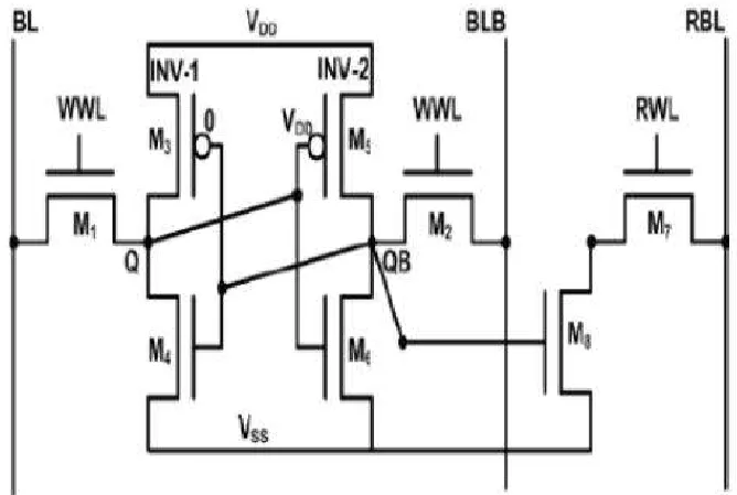
Shilpi Birla1 (2011) analysed 8T Static Random Access Memory cell at 65nm process technology is shown in figure.2. This topology was originally proposed for a sub threshold static RAM design and optimized for functionality and performance over a large voltage rang. A write operation is performed through WWL, WBL and WBLX port, whereas single ended read operation is exercised through RWL and RBL ports. RBL is pre charged at the end of each read cycle and keep pre charged during a write cycle. In this bit cell write and read ports are decoupled in contrast to the traditional 6T cell. Read-SNM problem is eliminated and 6T static RAM part can be sized for better write ability without trading off RSNM. This makes the voltage drop across unassessed read buffers zero and hence leakage on read bit line is highly reduced.
Figure.2 8T SRAM cell
Vdd is the virtual supply nodes for the cross coupled inverters and its voltage can be brought down during a write access to weaken PMOS load device and ease write ability problem at low voltage. Since all the bit cells on a row are written and read at the same time, Vdd is shared across one row of memory cells. J.Suganthi (2012) proposed the design as shown in the figure.3 operates fast as logic circuits operate and
Available online:
https://edupediapublications.org/journals/index.php/IJR/
P a g e | 302Figure.3 Zigzag 8T SRAM cell Two decoupled read port transistors NR0 and NR1, are
used to transfer the storage data Q and QB to the read bit line. The decoupled differential read port solves the read disturb issue. The zigzag 8T SRAM cell has better read static noise margins to the equivalent of hold SNM of conventional 6T static RAM. The zigzag 8T SRAM also has a faster read speed for long bit line application due to its small swing differential read sensing. Armin Tajalli and Yusuf Leblebici (2009)
proposed sub threshold SCL(source coupled logic) for low power SRAM and low activity rate digital systems. The subthershold leakage consumption of conventional CMOS circuits is more pronounced subthershold SCL can be used effectively for reducing the power consumption. A 9T memory cell has been developed to reduce the stand-by current while the SRAM array is operating at 2.1MHz clock frequency. Proposed 9T memory cell is shown figure 4.
Figure. 4 9T SRAM cell
The power consumption of the proposed circuit style is maintained in nanometre CMOS technology nodes. Mr. Sunil Jadav (2012) analysed ultra-low power 6T SRAM using adiabatic technique is shown in figure 5.
Available online:
https://edupediapublications.org/journals/index.php/IJR/
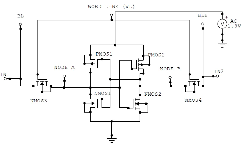
P a g e | 303Figure .5 6T proposed SRAM cell In this adiabatic technique ac power supply is used.By
using the ac power supply rather than dc the average power dissipation is reduced. Adiabatic switching can be achieved by ensuring that the potential across the Switching devices is kept aribitrarily small. Adiabatic charging may be achieved by charging the capacitor from time varying source that starts at VI=0V to Vdd.
A. Priadarshini (2013) proposed low power CMOS Static Random Access Memory based field programmable gate arrays architecture and analysed CMOS SRAMs that are used for on chip reconfiguration. This architecture is based on CMOS logic. Fast and low power SRAM based on 10T SRAM cells is shown in the figure 6.
Figure. 6 10T SRAM cell Compared to conventional 4T and 6T SRAM cells
delay is improved and the time for pre charged is reduced, 10T SRAM design avoids high switching
Available online:
https://edupediapublications.org/journals/index.php/IJR/
P a g e | 304Meenatchi Jagasivamani and Dong Sam Ha (2001)
analysed low power compiler with the capability to
choose between a low power and high speed SRAM. Structure of SRAM compiler is shown in figure.7.
Figure .7 Structure of SRAM compiler Overall average power dissipation is reduced and
substantial power over non-partitioned SRAM at the cost of speed and area.
Ankita Singh (2014) analysed the design of 8T SRAM using energy recovery logic and by using the energy
recovery logic cell stability, leakage noise has been improved. Figure 8 shows the 8T SRAM using energy recovery logic.
Figure.8 8T SRAM using energy recovery logic The proposed SRAM is structurally close to the
conventional CMOS SRAM. The PMOS transistor
Available online:
https://edupediapublications.org/journals/index.php/IJR/
P a g e | 305input from bit line. While the input voltage increases,
the other voltage depends on the circuit.
IV. CONCLUSION
An extensive survey has been done for various design of Static Random Access Memory. These designs are well preferred for various low power applications. Various techniques to reduce the power dissipation has been developed and it can be used for low power and high speed applications.
REFERENCES
[1] Akamatsu.H, Satomi.K, Suzuki.T, Yamagami.Y and Yamauchi.H,“A stable 2-port SRAM cell design against simultaneously read/write disturbed accesses” IEEE J. Solid-State Circuits, vol. 43, no. 9, pp.2109–2119,2008.
[2] Ankita Singh,”Analysis of 8T SRAM using Energy Recovery Logic”, IJERT, vol.3 Issue 2, feb 2014. [3] Anurag Dandotiya and Amit S. Rajput ,” SNM
Analysis of 6T SRAM at 32NM and 45NM Technique,” IJCA, vol.98, no.7, July 2014.
[4] Armin Tajalli and Yusuf Leblebici, ”Subthreshold SCL for Ultra-Law-Power SRAM and Low-Activity-Rate Digital Systems,”
[5] J. Caravella, “A Low Voltage SRAM For Embedded Applications,” IEEE Jourrial of Solid-state Circuits, Vol. 32, No. 3, pp. 428- 432, Mar.1997.
[6] V. Gupta, M. Anis,“Statistical design of the 6T SRAM bit cell”, IEEE Trans. Circuits Syst. I, Vol. 57, No. 1, pp. 93–104, Mar. 2010.
[7] Meenatchi Jagasivamani and Dong Sam Ha, “Development of Low Power Compiler”, 2001.
[8] Nahid Rahman and B. P. Singh, ”Design and Verification of Low Power SRAM using 8T SRAM Cell Approach,” IJCA, Vol. 67, no.18,April 2013. [9] Naveen Verma,”Ultra-Low-Power SRAM Design In High Variability Advanced CMOS,” May 2009. [10] A.Priadarshini, ”Low power reconfigurable FPGA based on SRAM,” ICCCI , Jan 2013.
[11] Saurabh Neemgaonkar, Anshul Jain, Vijay Kumar Magraiya,” Comparative Analysis of Low Power 8T SRAM,” IJECT, vol.4, Issue-4,2013. [12] Mr. Sunil Jadav, Mr. Vikrant, Dr. Munish