Western University Western University
Scholarship@Western
Scholarship@Western
Electronic Thesis and Dissertation Repository
4-17-2014 12:00 AM
Quantum Optics of Polaritonic Nanocomposites
Quantum Optics of Polaritonic Nanocomposites
Chris Racknor
The University of Western Ontario
Supervisor Mahi R. Singh
The University of Western Ontario
Graduate Program in Physics
A thesis submitted in partial fulfillment of the requirements for the degree in Doctor of Philosophy
© Chris Racknor 2014
Follow this and additional works at: https://ir.lib.uwo.ca/etd
Part of the Condensed Matter Physics Commons, Optics Commons, and the Quantum Physics Commons
Recommended Citation Recommended Citation
Racknor, Chris, "Quantum Optics of Polaritonic Nanocomposites" (2014). Electronic Thesis and Dissertation Repository. 2002.
https://ir.lib.uwo.ca/etd/2002
QUANTUM OPTICS OF POLARITONIC NANOCOMPOSITES
(Thesis format: Integrated Article)
by
Christopher D.C. Racknor
Graduate Program in Physics
A thesis submitted in partial fulfillment
of the requirements for the degree of
Doctor of Philosophy
The School of Graduate and Postdoctoral Studies
The University of Western Ontario
London, Ontario, Canada
ii
Abstract
In this thesis, we study the quantum optical interaction in polaritonic nanocomposites.
These systems are made by the combination of two or more micro- or nano-scale structures with
complementary optical properties, such as polaritonic materials, excitonic materials, photonic
crystals (PCs), quantum dots (QDs), waveguides, couplers, metal nanorods (MNRs),
bionanoparticles. The nanocomposites systems studied included QDs doped within a polaritonic
PC, an excitonic waveguide coupler, and a metamaterial waveguide. Also addressed are systems
consisting of MNRs paired with biological labelling dye or QDs.
The application of a strain field, known as the acousto-optic effect, was found to control
photon transmission in polaritonic PC, and through that, the spontaneous emission of a QD
doped within the crystal. Furthermore, a theory of reservoir induced-transparency (RIT) was
developed in the QD-exciton-polaritonic coupler and QD-metamaterial waveguide
nanocomposites. Transparent states in the absorption spectrum of the QD can be induced via the
presence of bound polariton states in the coupler/waveguide. The nature of the states could be
controlled by the separation of the couplers or the thickness of the metamaterial.
Energy transfer is found and an explanatory theory is developed for MNRs with
QD/biological labelling dye nanocomposites. Decrease in fluorescence lifetime from the dye is
shown to be greater for excitation through that two-photon process. Increase of two-photon
intensity is shown to significantly increase enhancement of the energy transfer.
Keywords
Polaritonics, phonon-polariton, exciton-polariton, surface plasmon-polariton, nanocomposites,
photonic crystals, quantum dots, metal nanorods, metamaterials, Schrödinger equation method,
iii
Co-Authorship Statement
This thesis contains both material from previously published manuscripts and
unpublished results.
For the material presented in chapters 3, 4, & 6, Chris Racknor and Mahi Singh
developed the theoretical formalism and wrote the manuscripts. Chris Racknor performed the
numerical calculations and produced the results in consultation with Mahi Singh.
In chapter 5, Chris Racknor and Mahi Singh developed the theoretical formalism and
wrote most of the manuscript. Chris Racknor performed the numerical simulations and produced
the results in consultation with Mahi Singh. Yu Chen wrote the portions of the manuscript
pertaining to the experimental methods. Yinan Zhang, David Birch and Yu Chen performed the
experimental work.
In chapter 7, Chris Racknor and Mahi Singh developed the theoretical formalism and
wrote the manuscript. Chris Racknor performed the numerical simulations and produced the
results in consultation with Mahi Singh. Marek Brzozowski produced the first three figures and
iv
v
Acknowledgments
My foremost appreciation goes to Professor Mahi Singh, for his support and patience
during my graduate degree. I was fortunate to have a supervisor with so much time for his
graduate students to discuss research projects and answer questions. His guidance saw me
through to the completion of this thesis.
I would like to thank my graduate school compatriots Joel Cox, Graeme Bart, I. Haque,
Ali Hatef, Daniel Schindel, and Marek Brzozowski for their friendship and support. I may never
have got myself through the experience without their camaraderie and inspiration, and it
wouldn't have been anywhere near as enjoyable without them.
My appreciation goes out to every faculty, staff member, and student in the department of
Physics and Astronomy at Western University during my time. Ending with this thesis I have
spent three months shy of an entire decade there and there is not a single soul that has not
contributed to my journey in some way. Thank you.
I would also like to thank parents for their love and support allowing me to make
education my job for so long. I also thank my brother, Andrew, for his love and for keeping me
grounded.
I owe the most in these last years to my wife and partner, Kristina, for her immeasurable
love, support, and encouragement. Without her I do not know what I ever would have become.
And lastly, my daughter Adelaide, she put the guarantee of joy into the rest of my life and the
vi
Table of Contents
Abstract ... ii
Co-Authorship Statement ... iii
Acknowledgments ... v
Table of Contents ... vi
List of Abbreviations ...
viii
List of Figures ... ix
1
Fundamentals ... 1
1.1
Polaritons ... 1
1.2
Structures ... 5
1.3
Processes ... 10
2
Introduction ... 13
2.1
Phonon-Polaritonic Nanocomposites ... 13
2.2
Exciton-Polaritonic Nanocomposites ... 16
2.3
Plasmon-Polaritonic Natural Material Nanocomposites ... 18
2.4
Plasmon-Polaritonic Metamaterial Nanocomposites ... 19
2.5
Objective and Outline of Thesis ... 21
3
Acousto-Optics in Polaritonic Photonic Crystal Nanocomposites ... 31
3.1
Introduction ... 31
3.2
Theoretical Formalism ... 32
3.3
Results and Discussion ... 39
3.4
Conclusions ... 48
4
Reservoir Induced Transparency in Exciton Polaritonic Nanocomposites ... 53
vii
4.2
Theoretical Formalism ... 55
4.3
Results and Discussion ... 64
4.4
Conclusions ... 72
5
Fluorescence in Biological Labelling Dye-Gold Nanorod Nanocomposites ... 75
5.1
Introduction ... 75
5.2
Experimental Methods ... 78
5.3
Theoretical Formalism ... 80
5.4
Results and Discussion ... 85
5.5
Conclusions ... 87
6
Nonlinear Energy Transfer in Quantum Dot-Metal Nanorod Nanocomposites .. 91
6.1
Introduction ... 91
6.2
Theoretical Formalism ... 93
6.3
Results and Discussion ... 99
6.4
Conclusions ... 105
7
Surface Plasmon-Polariton Induced Transparency in Metamaterial Waveguide
Nanocomposites ... 110
7.1
Introduction ... 110
7.2
Theoretical Formalism ... 113
7.3
Results and Discussion ... 122
7.4
Conclusions ... 126
8
Concluding Remarks ... 129
Copyright and Reprint Permissions ... 132
viii
List of Abbreviations
AFD
Alexa Fluor Dye
BEP
Bound Exciton-Polariton
CRLH
Composite Right/Left Handed
DDI
Dipole-Dipole Interaction
DOS
Density of States
EIT
Electromagnetically Induced Transparency
ETR
Energy Transfer Rate
GNR
Gold Nanorod
MNR
Metallic Nanorod
PC
Photonic Crystal
QD
Quantum Dot
RIT
Reservoir Induced Transparency
SPP
Surface Plasmon-Polariton
TE
Transverse Electric
List of Figures
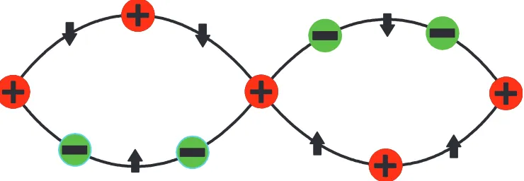
11 Graphical representation of the optical mode of a phonon. Here, the + and
-represent the charge on the ions in the material. The arrows show the directions
of motion of the mode. . . 2
1-2 Diagram of the formation of an exciton (electron-hole pair) being excited from
the valence to the conduction band by an incident photon. . . 3
1-3 Diagrams of surface plasmons along an interface between a metal and a dielectric 5
1-4 Sample dispersion relation for a phonon-polaritonic material. The red line is the
light line, it shows the uncoupled dispersion of the photon. The black lines are
the coupled dispersion relation. Note the band gap. This is the region of photon
energies that are forbidden to propagate in the material. The further from the
band gap, the more the polariton will act like an uncoupled photon. The closer
to the band gap, the more the polariton will act like an uncoupled phonon. . . . 6
1-5 Potential geometries for 1D, 2D, and 3D photonic crystals. . . 7
1-6 This photonic crystal is made by making periodic holes in a dielectric material.
The waveguide is made by leaving a path through the dielectric that is free of
holes. . . 9
1-7 Energy level diagram of the two-photon process. The electron will absorb two
photons of energy }!1 to taken from the ground to excited state. Once the electron decays back to the ground state, aka ‡uorescence, it will emit one photon
3-1 2-D cross-sectional view of the considered 3-D polaritonic photonic crystal. The
photonic crystal is air spheres periodically arrange in a polaritonic crystal
back-ground. The periodicity is denoted by the lattice constant, L, and the radius of the air spheres is rs. . . 33
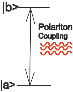
3-2 Schematic of the two level quantum dot. The ground state isjaiand the excited state is jbi. It is coupled to the phonon-polaritons in the polaritonic photonic crystal. . . 37
3-3 The dielectric constant, , is plotted as function of energy, "k. The solid curves
corresponds to GaP, the dashed curve to MgO, the dotted to LiNbO3, and the
alternating dots and dashes to LiTaO3. . . 40
3-4 The dispersion relation is plotted as function of normalized wave vector. The
crystal parameters are taken as L = 200 nm and 2L=a = 0:3. (a) The solid curves corresponds to GaP and the dashed curve to MgO. (b) The dotted line
corresponds to LiNbO3 and the alternating dots and dashes to LiTaO3. . . 41
3-5 The lower band edge energy,"v, of GaP is plotted as a function of acoustic strain
intensity. The solid line represents "v for I = 0 W/m2 and the dashed line for
varyingI from I = 106 W/m2 toI = 109 W/m2. . . 43 3-6 The DOS is plotted as a function of photon energy of the quantum dot. The
crystal parameters are taken as L = 200 nm and 2L=a = 0:3. (a) The solid curves corresponds to GaP and the dashed curves to MgO, respectively. (b) The
dotted lines correspond to LiNbO3 and the alternating dots and dashes to LiTaO3. 44
3-7 The DOS is plotted as a function of photon energy of the quantum dot for varying
strain intensity, I. The solid line corresponds to LiNbO3 when I = 0W/m2 and
the dashed line corresponds to I = 109 W/m2 where (a) shows the lower band
and (b) shows the upper band. . . 45
3-8 The transmission coe¢cient is plotted as a function of energy for LiNbO3. The
solid curve corresponds to when strain intensity I = 0:0 W/m2 and the dashed curves corresponds to I = 109 W/m2. (a) shows the lower band edges and (b)
shows the upper band edges. . . 46
3-10 The DOS is plotted as a function of acoustic strain intensity for speci…c values
of the photon energy for LiNbO3. (a) depicts the lower band of the DOS. The
solid line is for photon energy " = 0:530 eV, the dotted line for " = 0:535 eV, and the dashed line for"= 0:540eV. (b) shows the upper band of the DOS. The solid line is for photon energy " = 1:030 eV, the dotted line for " = 1:035 eV, and the dashed line for "= 1:040eV. . . 48 4-1 Schematic of the Coupler system. Material A taken to beCdS and material B is
taken to beZnO. The small orange spheres are the quantum dots doped within theCdS layers . . . 55 4-2 Dispersion relations of (a)ZnOand (b)CdS. The curves show the energy of the
exciton-polaritons,", versus their wavevector,k. Band gaps can be seen between energies "T1 &"L1 and "T2 &"L2 where there are no possible exciton-polariton
energy states. . . 56
4-3 Schematic of the four-level N-type QD system.
58
4-4 The bound state energies as a function of separation,h, between theCdS layers in the coupler (dashed line). The dotted line shows the single uncoupled BEP
energy, "n= 3:384eV.
65
4-5 Plot of the DOS (in arbitrary units) of the coupler as a function of Energy (eV)
within the band gap of ZnO. 66
4-6 The time evolution of ab is plotted for the value of ab= 1 for probe detuning.
The dotted curve showsh= 150 nm and the dashed curveh= 80nm. 67
4-7 The o¤ (solid curve) and on (dotted curve) resonance absorption forh= 150nm coupler separation of the QD plotted against probe laser detuning, ab (meV).
4-8 The o¤ (solid curve) and on (dashed curve) resonance absorption forh= 80nm coupler separation of the QD plotted against probe laser detuning, ab (meV).
69
4-9 The e¤ect of the control laser c applied to the jci $ jdi transition on the
ab-sorption of the QD plotted against probe laser detuning, ab (meV), in the case
of the coupler with separation h = 80 nm. For the dashed curve c = 0 and c = 0:1 b for the alternating dashes and dots curve.
70
4-10 The non-resonant absorption (solid curve), theh = 150 nm (dotted curve) and
h = 80 nm (dashed curve) coupler separation resonant absorption of the QD plotted against probe laser detuning, ab (meV).
70
4-11 The (a) delay timeTdel, and (b) group velocity dispersion coe¢cient,D, plotted
against detuning, ab. In both the dotted curve corresponds to the coupler in
case h= 150nm and the dashed to h= 80nm.
71
5-1 Schematic diagram of Alexa Fluor405-gold nanorod hybrid system. . . 77
5-2 The spectrum of Alexa Fluor 405 and mixture samples, S0-1 and S0-2, excited
at 385nm. . . 79
5-3 Normalized theoretical and experimental ‡uorescence intensity under one-photon
excitation. . . 85
5-4 Normalized theoretical and experimental ‡uorescense intensity under two-photon
excitation. . . 86
6-1 A schematic diagram of the QD and MNR. Here R is distance between the QD and the MNR when the QD lies along a) the minor axis, sa = 1, or b) the
major axis, sa= 2, of the MNR. Three exciton levels of QD are denoted by j1i,
j2i, and j3i. Probe and control …elds are applied to monitor the j1i $ j2i and
6-2 The energy transfer rate, WMQD, plotted vs probe detuning 4p. The intensity
of the probe …eld is Ip = 1 W=cm2, the separation is R = 12 nm, and sa = 2.
The dotted and dashed curves are plotted for intensity of the control …eld being
Ic = 0 GW=cm2 and Ic = 45GW=cm2, respectively. . . 100
6-3 The energy transfer rate,WMQD, plotted vs probe detuning4p. The intensity of
the control …eld is Ic = 45 GW=cm2, the separation is R = 12 nm, andsa = 2.
The dotted and dash-dotted curves are plotted for intensity of the control …eld
beingIp = 1 W=cm2 and Ip = 3 W=cm2, respectively. . . 102
6-4 The energy transfer rate,WMQD, plotted vs probe detuning4p. The intensity of
the control …eld isIc = 45GW=cm2, the separation isR= 12nm, andsa= 1.
The dotted and dash-dotted curves are plotted for intensity of the control …eld
beingIp = 1 W=cm2 and Ip = 3 W=cm2, respectively. . . 103
6-5 The energy transfer rate,WMQD, plotted vs probe detuning4p. The intensity of
the probe …eld is Ip = 0:3 W=cm2, the separation is R = 12 nm, and sa = 2.
The dotted and dashed curves are plotted for intensity of the control …eld being
Ic = 0 GW=cm2 and Ic = 45cW=cm2, respectively. . . 104
6-6 The energy transfer rate, WMQD, plotted vs centre-to-centre separation of the QD-MNR system R. The dotted curves is drawn for probe and control …elds of
Ip = 1 W=cm2 and Ic = 0 GW=cm2, the dashed curve for Ip = 1 W=cm2 and Ic = 45GW=cm2 …elds, and the dash-dotted curve for Ip= 3 W=cm2 andIc = 0 GW=cm2. Here4p = 4s and sa = 2. Inset: ETR vs control …eld intensityIc
forIp = 1 W=cm2,4p = 4s,sa= 2, and R= 12nm. . . 105
7-1 Schematic of the QD-metamaterial waveguide nanocomposite. The waveguide is
made of a CRLH metamaterial between two layers of polyethylene. The
poly-ethylene layers are doped with QDs. . . 112
7-2 The unit cell of the CRLH metamaterial used in the fabrication of the waveguide.113
7-4 The dispersion relation for the (a) TM and (b) TE modes of the metamaterial
waveguide. Dotted curves corresponds to metamaterial wheredm 400nm, and
dashed curves to dm = 400nm.
123
7-5 The absorption coe¢cient ( = 0) of the QD of the probe detuning for the (a) TM
and (b) TE modes of the metamaterial waveguide. Dotted curves corresponds
to metamaterial where dm 400nm, and dashed curves to dm = 400nm. Inset:
Chapter 1
Fundamentals
In this chapter the fundamental concepts required in the thesis are presented. Providing a
more indepth look at the components, structures, and processes used will give the reader an
improved base with which to better understand the thesis as it is written.
1.1
Polaritons
Polaritons are quasiparticles resulting from electric or magnetic dipole-carrying excitations
within a material strongly coupling to electromagnetic waves that travel within them. Thus,
the photons of light moving within a dispersive, or polaritonic, material are not freely
prop-agating but are held back by their interaction with the present dipoles. This forms what is
known in quantum optics as a dressed state where the photon is in essence "dressed" with the
material excitation. An important feature of polaritonic materials is the formation of photonic
band gaps in the dispersion relation of the material without any constructed periodicity in
the material structure. Bands of energies forbidden to travel in the material occur when the
coupling between the photons and the medium’s excitations are approximately at resonance.
The condition of resonance we refer to is that of both waves having nearly equal frequencies
and wavevectors [1].
A few such sources of dipole carrying excitations are excitons, optical phonons,
surface-plasmons, and magnons. By their di¤erent manner of coupling with light in the formation of a
Figure 11: Graphical representation of the optical mode of a phonon. Here, the + and -represent the charge on the ions in the material. The arrows show the directions of motion of the mode.
will propagate within them. Of these excitations, the …rst three will be addressed in this thesis.
1.1.1 Phonon-Polaritons
Phonon-polaritons are the result of photons interacting with transverse optical phonons [1].
In some literature they are sometimes referred to as just polaritons. Optical phonons may only
be found in materials with more than one type of atom in their unit cell. The optical phonon
is the out-of-phase oscillation of the oppositely charged atoms in the lattice creating a
time-varying dipole moment. Adjacent atoms are always moving in opposite directions. A visual
representation is shown in Fig 1-1. The acoustic mode, which is the two di¤erent atoms move
together, does not result in a dipole excitation to which photons may couple. Optical phonons
are excited by infrared radiation and will interact with photons with frequencies between 100
GHz and 10 THz to form phonon-polaritons. Examples of dispersive materials which will
support the formation of phonon-polaritons are GaP, MgO, LiNbO3, LiTaO3, NaCl, GaAs, and
LiH. The …rst four of these will be used in the studies performed in this thesis.
1.1.2 Exciton-Polaritons
Exciton-polaritons are, as their name suggests, the coupled interaction of photons with excitons
within a material [2]. Excitons are most commonly found in insulators and semiconductors.
Figure 1-2: Diagram of the formation of an exciton (electron-hole pair) being excited from the valence to the conduction band by an incident photon.
atomic lattice, called the conduction band, and where they are con…ned to their individual
atoms, called the valence band. They are commonly known as excitonic materials. Within
both bands the electronic states are arranged into discrete levels that depend on the size and
shape of the structure containing them. Commonly, there is a region between these bands called
the electronic band gap. Similar to the photonic band gap, these are energies where no electron
states are allowed to exist. An exciton is made by an absorbed photon exciting an electron
from the valence band into the conduction band leaving behind a positively-charged electron
hole, as shown in Fig 1-2. This creates a dipole in which the photon will couple with to create
an exciton-polariton. They are also sometimes also referred to as ‘dressed excitons’.
1.1.3 Surface Plasmon-Polaritons
The last of the polaritons of interest are surface plasmon-polaritons. Plasmons are
de-scribed in a classical picture as the collective oscillation of the free electrons with respect to
the positive ions in a metal [3]. The oscillation will proceed with at what is called the
plas-mon frequency. They exist in the bulk of a metal or along its surface. Surface plasplas-mons are
con…ned to the surface of a metal and strongly interact with photons resulting in a polariton.
Surface plasmon-polaritons have tight spatial con…nement and may be present along a ‡at two
dimensional interface or along the outer surface of …nite sized metallic nanostructures. A visual
representation of surface plasmon-polaritons propagation in both situations is shown in Fig
or visible light ranges.
1.1.4 Dispersion relation
The dispersion relation of each type of polariton will change in a di¤erent manner with the
frequency of incident light.
"= }c
n(")k
Here "is the energy of polaritons in the material whilek is their wavevector. c is the speed of light and n(") is the refractive index of the polariton material. You’ll note that the refractive index depends on the energy of the polaritons. The manner in which nvaries with"will di¤er for each di¤erent type of polariton. A graphical representation of the dispersion relation of a
phonon-polariton is shown in Fig 1-4 where there are two bands of propagation separated by
a band gap. Near the band gap the polariton acts more phonon-like and away from the gap
more photon-like. Dispersion relations for exciton-polaritons and surface plasmon-polaritons
Figure 1-3: Diagrams of surface plasmons along an interface between a metal and a dielectric
1.2
Structures
To facilitate the creation and investigate the e¤ects these polaritons, structures are needed
in which to study them. In this thesis, as in the whole study of nanocomposite hybrid systems,
there are a multitude of possible components to choose from. We have used photonic crystals,
waveguides, quantum dots, metal nanorods, biological labeling dye, and metamaterials to do
our studies.
1.2.1 Photonic Crystals
Photonic crystals are a very recently developed structure made to localize and control the
‡ow of light within it [4]. They are materials made with the periodic arrangement of dielectric
materials with di¤ering dielectric constants and this periodically may be in one, two, or three
spatial dimensions. A visual representation of this is shown in Fig 1-5. In one dimension,
Figure 1-4: Sample dispersion relation for a phonon-polaritonic material. The red line is the light line, it shows the uncoupled dispersion of the photon. The black lines are the coupled dispersion relation. Note the band gap. This is the region of photon energies that are forbidden to propagate in the material. The further from the band gap, the more the polariton will act like an uncoupled photon. The closer to the band gap, the more the polariton will act like an uncoupled phonon.
this structure cause an energy gap to appear in its photonic dispersion relation. Just as the
polaritonic band gaps, this makes for a speci…c range of frequencies forbidden to propagate in
the photonic crystal. Though reliant on the particular construction of the photonic crystal,
the band gap has the potential for customization that polaritonic band gaps, which are mostly
limited to the nature of the chosen dispersive material, lack. Photonic crystals do present a
potential photonic analogue to semiconductors for optical devices.
One dimensional photonic crystals are easily made by growing layers of alternating dielectric
materials on top of each other. A 2-D photonic crystal may be made by growing an array of
nanorods out of one material then …lling the area between them. Lastly, one possible method for
creating a three-dimensional photonic crystal is to periodically arrange spheres of a material in
a container then and …ll the empty space with another material to act as the background. Once
the spheres are dissolved this is a with photonic crystal made from air spheres in a background
Figure 1-5: Potential geometries for 1D, 2D, and 3D photonic crystals.
1.2.2 Quantum Dots
Quantum dots are a semiconductor component that is as important to photonics as it is to
electronics [5]. They are a three-dimensional semiconductor nanostructure that will con…ne its
excitons in all three spatial dimensions. At typically spheres of size less than 3 nm in diameter
quantum dots have electronic characteristic, such as electronic band gap and energy levels,
closely tied to their size and shape and thus they are highly tunable. Even though they are
semiconductors and contain excitons, exciton-polaritons do not propagate within them because
of their extremely small size. Fluorescence occurs in quantum dots when an exciton recombines
with its hole and emits a photon, which can also be described as the excited electron decaying
back down to its ground state. The light will have an energy equal to the di¤erence between
the excited and ground states.
Spontaneous emission is the term given to the process whereby this electron will decay
to the ground state without being stimulated to do so. The rate at which the exciton will
recombine once excited is called the decay rate and is described by Fermi’s golden rule. The
density of states, which is the number of available photon per unit energy in the system and
depends on the derivative of its dispersion relation with respect to energy. Thus, the properties
of the quantum dot may also be changed by manipulating the surrounding material. The ability
of quantum dots to be doped into other structures makes them very e¤ective for probing the
optical properties of those structures. If the surrounding material has a band gap within which
the emitted energy would exist (i.e. a photonic or polaritonic crystal) the emission would be
suppressed and the photon would be con…ned to the quantum dot. This may also be used to
allow emission only in certain spatial directions.
Quantum dots can self assemble under certain circumstances through molecular beam
epi-taxy in a process called Stranski–Krastanov growth. When a material is grown on a substrate
without matching the two lattices it is strained and will collect into small ‘islands’ instead of
as a smooth layer. Normally this island formation is something to be avoided as it would ruin
multiple layer materials. However, these islands make for excellent quantum dots once they are
buried in a material with an electron band gap. Quantum dots can also be made from core-shell
structures where colloidal chemistry methods produce one semiconductor crystal wrapped in
another. Notable core-shell pairs are CdS/ZnS, CdSe/ZnS, CdSe/CdS, and InAs/CdSe [5].
1.2.3 Waveguides
Another structure to manipulate the ‡ow of light in a system is a waveguide [6]. A
waveguide can be any structure that con…nes light to only travel in one or two spatial
di-rections. One that con…nes light only in one direction is often referred to as a …ber waveguide,
those that con…ne to two are called slab waveguides. Any of these types of waveguides consist
of two parts: a core region that allows the light to ‡ow and a cladding region that provides
the con…nement. Construction of two waveguiding components close enough to couple yet still
separated by a cladding region is called a coupler. These couplers may have as any number
of coupled layers making for a range of di¤erent propagation possibilities. Waveguides can be
structured with a high index of refraction material surrounding one of lower index. The
con-…nement of the optical waves in these types of waveguides is by total internal re‡ection. This
is how modern …ber optic cables work. A more e¢cient con…nement mechanism is one using
Figure 1-6: This photonic crystal is made by making periodic holes in a dielectric material. The waveguide is made by leaving a path through the dielectric that is free of holes.
exists within the band gap of the cladding. Polaritonic crystals can be made into a waveguiding
structure such as this by either layering one crystal between slabs of another or wrapping a wire
of one with the other. You can also take one built with either one, two, or three dimensions of
periodicity and remove one or more layers of one of the alternating dielectrics. An example is
shown in Fig 1-6 for a waveguiding region in a 2-D photonic crystal.
1.2.4 Metamaterials
In the pursuit of better waveguiding capabilities and novel optical properties researchers
have come to develop arti…cial materials, known as metamaterials, to aid them in their work.
They are developed for the expressed purpose of …nding new properties that are not found in
nature. One such property is negative index of refraction. This concept has been popularized
for its science …ction inspiring potential to create a cloaking device. Built around a unit cell
structure that is smaller than the wavelength of light by which you want to interact with,
create a material whose permittivity and permeability are dependent on the frequency of the
incident light, much like in metals, polaritonic materials, and photonic crystals. This makes it
possible to …nd a region in which both permittivity and permeability are negative. Plasmonic
metamaterials contain surface plasmons to couple and interact with incident light. Interaction
will give rise to SPPs and these metamaterial would be highly tunable and customizable in
application [3].
The plasmonic metamaterial of interest to this thesis is a composite right/left handed
(CRLH) metamaterial. This metamaterial is made using capacitors and inductors.
Right-handed materials are those within which the electric and magnetic …elds, and the direction
of propagation of light obeys the right hand rule. In left-handed materials the direction of
propagation is the opposite, thus the waves in that kind of material would obey the left-hand
rule. The unit cell of a CRLH metamaterial is one that contains an equivalent circuit of both
right-handed and left-handed natures. A schematic of this unit cell can be found in Fig 7-2.
Depending on the frequency of interaction, it may show right-handed or left-handed behaviour
[7].
1.3
Processes
1.3.1 The Acousto-Optic E¤ect
In this work we have utilized a few methods for interacting with our hybrid system
compo-nents. The acousto-optic e¤ect is a method for altering the refractive index by the application
of a strain …eld to the crystal [8]. Since phonon-polaritons are mitigated by optical phonons,
the acousto-optic e¤ect is a speci…c case of photoelasticity whereby a mechanical strain …eld
will change the permittivity of a material. This would have an e¤ect on the dispersion relation
in the material and potentially change the location of the band gap.
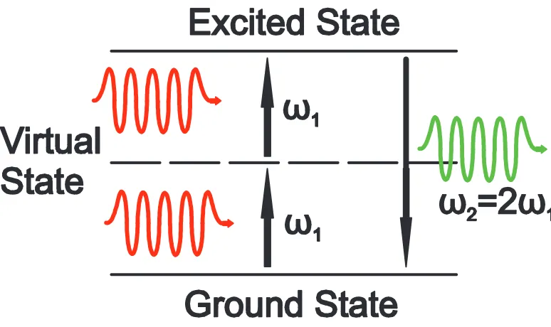
1.3.2 Two-Photon Process
Two-photon absorption is a nonlinear optical process by which two photons are simultaneously
absorbed to excite an electron from one state to another [9]. The energy di¤erence between the
Figure 1-7: Energy level diagram of the two-photon process. The electron will absorb two photons of energy }!1 to taken from the ground to excited state. Once the electron decays back to the ground state, aka ‡uorescence, it will emit one photon of energy }!2=2}!1.
high light intensity, which was not available to researchers until the invention of the laser.
Two-photon absorption occurs without the presence of an intermediate state, though it can be
treated as a “virtual” state facilitates the transition. This is shown in Fig 1-7. Two-photon
excited ‡uorescence, or simply a two-photon process, is the action of exciting a transition with
two photons that will then be emitted as one photon with energy that is the sum of the two
incident photons. Two-photon processes are important to bioimaging because the human body
is opaque to visible wavelength of light. Using two-photon absorption with ‡uorescent dyes in
biological situations allows one to use the far infrared region of the spectrum to image living
tissue. Two-photon microscopy has deeper tissue penetration, more e¢cient light detection,
Bibliography
[1] C. Kittel, Introduction to Solid State Physics, (John Wiley & Sons Inc., New York, 1986).
[2] D. Sanvitto and V. Timofeev, Exciton Polaritons in Microcavities, (Springer, Berlin, 2012).
[3] M.R. Singh, Electronic, Photonic, Polaritonic and Plasmonic Materials, (Wiley Custom,
Toronto, 2014).
[4] J.D. Joannopoulos, S.G. Johnson, J.N. Winn, and R.D. Meade, Photonic Crystals: Molding
the Flow of Light, 2nd Ed. (Princeton University Press, 2008).
[5] V.I. Klimov, Nanocrystal Quantum Dots, 2nd Ed. (CRC Press, 2010).
[6] K. Okamoto, Fundamentals of Optical Waveguides, (Elsevier Academics Press, Burlington,
MA, 2006).
[7] C. Caloz and T. Itoh, Electromagnetic Metamaterials (Wiley Interscience, Hoboken, New
Jersy, 2006).
[8] A. Yariv and P. Yeh, Photonics (Oxford Univerity Press, New York, 2007).
[9] R.W. Boyd, Nonlinear Optics (Academic Press, 2008).
[10] P.J. Campagnola, H.A. Clark, W.A. Mohler, A. Lewis, and L.M. Loew, J. Biomed. Opt.
Chapter 2
Introduction
In the previous chapter we explained the fundamental physics required to understand this
thesis. The concepts such as those of polaritonic materials, quantum dots, photonic crystal,
and metamaterials are all addressed. This chapter will present an overview of the research
literature covering the material studied in this thesis.
2.1
Phonon-Polaritonic Nanocomposites
Polaritonic materials represent a vast potential for bridging the gap between photonics and
electronics research in the creation of unique and e¢cient optoelectronic devices.
Nanocom-posites are systems made by combining two or more micro- or nano-scale structures to have
capabilities beyond those of each component. Those containing polaritonic material will be an
important component of future quantum optics research. Nanocomposites are also known as
hybrid systems. Phonon-polaritonic materials operate at frequencies ranging from hundreds of
GHz to several THz in the regime connecting photonics and electronics. Polaritons are
qua-siparticles formed in the strong coupling interaction of an incident transverse electromagnetic
wave photons with transverse optical phonons in the host material. Signi…cant to their
oper-ation, polaritonic materials have a range of photon energies that are forbidden to propagate
in them, called a photonic band gap, that arises naturally out of the resonant coupling of the
phonons and photons [1].
photonic counterparts to electronic devices such as transistors, sensors, and integrated circuits
that exploit the well known speed advantage in photons over electrons. These materials have
also been explored for applications in high-bandwidth signal processing, THz imaging and THz
spectroscopy [2],[3].
Maragkou et al. [4] have proposed that polaritonic materials may be used to create lasers
that operate at reduced thresholds making them more e¢cient to use. Polariton band gaps in the
THz range have been studied in periodic and quasi-periodic multilayer systems [5]. Re‡ection
and absorption measurements have also been obtained for polaritonic materials in the
THz-frequency range [6]. Polaritonic waveguides and resonators have been fabricated from LiNbO3
and LiTaO3 host crystals [2],[3],[7], while polaritonic wires made from an isotropic dielectric
material coated with metal have also been investigated [8]. It has been shown that suppression
of spontaneous emission occurs when a quantum dot is placed within a polaritonic material
[9],[10], and the optoelectronic behaviour of a polaritonic nanowire is optimal to developing
all-optical switches [11].
Photonic crystals are another well known advance in photonic devices. Realized in 1987 [12],
they are structures with a periodic arrangement of dielectric materials with di¤ering dielectric
constants. This structure was found to cause an energy gap to appear in the photonic dispersion
relation. Again, this is a range of energies that would be forbidden to propagate in the crystal.
This range is determined by the constrast between the pair of dielectric materials and the
spacing distances. This gives some control over the band gap to the researcher in fabrication.
There is a problem though in how high a contrast is actually required to form a full photonic
band gap [13]. For example, inverse opal photonic crystals require dielectric contrast of a factor
of eight to obtain a photonic band gap in the optical regime. This restriction causes a great
deal of di¢culty in terms of fabrication. Materials with energy dependent dielectric constants,
such as polaritonic materials, are the best alternative to overcome this barrier. This work will
consider photonic crystals fabricated using polaritonic materials.
There has been some recent work done on polaritonic photonic crystals [14]-[24]. Huang et al.
[14]- [16] have demonstrated that polaritonic photonic crystals will exhibit near-dispersionless
bandwidth …eld localization in the polaritonic material and metal-like bands with complete ‡ux
Sigalas et al. [17] have calculated the transmission coe¢cient for a 2-D square lattice of GaAs
and air and found it to have a band gap to be in the THz range. Zeng et al. [18] have used
2-D polaritonic photonic crystals as waveguides, and showed that propagation loss decays with
increasing waveguide wall thickness. Högström and Ribbing [19] have veri…ed the presence of
a polaritonic band gap for thicknesses of 1-D photonic crystals lower than the wavelength for
SiO2/Si and SiO2/air.
Furthermore, Kuzmiak et al. [20] calculated the photonic band structure for an in…nite
array of polaritonic rods in a vacuum. They found that for larger values of the volume …lling
fraction, the dispersion relation produced a complete 2-D photonic band gap for transverse
electric electromagnetic waves. Rung and Ribbing [21] showed that in a polaritonic photonic
crystal, the photonic gap can be shifted across the polaritonic gap by varying the crystal’s
lattice constant. Chern et al. [22] used an interfacial operator approach to study the e¤ect of
structural and polaritonic parameters on four di¤erent polaritonic photonic crystal structures.
Gantzounis and Stefanou [23] used layer-multiple-scattering to study the optical properties of
3-D polaritonic photonic crystals and their transmission characteristics. In addition, they [24]
also studied and the optical response of …nite slabs of 2-D and 3-D periodic structures of air
cavities in polaritonic materials, which revealed existence of strong resonant modes.
The acousto-optic e¤ect is a method capable of altering the refractive index by the
appli-cation of a strain …eld to a material. This is of particular interest to polaritonics research since
the polariton is formed by photons coupling to phonons. Changing the refractive index would
change both the natural photonic band gap of the polaritonic material but also the band gap of
any photonic crystal that material was part of. The photon transmission of some wavelengths
of light could then be changed.
Research into the acousto-optic in photonic crystals has already found promising results
[25]-[27]. For example, Courjal et al. [25] have studied an active 2-D lithium niobate photonic
crystal driven by stationary Rayleigh surface acoustic waves. The con…guration relies on two
in-terdigital transducers that modulate the refractive index through the acousto-optic e¤ect. Their
experiments showed a signi…cant enhancement of the elasto-optical interaction. Haakestad and
Engan [26] have studied experimentally the acoustic and acousto-optic properties of a solid core
to the …rst higher order optical modes of the solid core …ber. Lim et al. [27] have measured the
multiple resonance peaks in an all-…ber acousto-optic tunable …lter built with a photonic crystal
…ber. They explained their experiments by using the physics of acousto-optic mode coupling.
2.2
Exciton-Polaritonic Nanocomposites
There is signi…cant research interest in the optoelectronic interaction of nanocomposites
[28]-[32]. These hybrid systems can consist of many combinations of nanoscale components, such as
graphene [28], metallic nanoparticles [29], metamaterials [30], quantum dots [29] and nanowires
[31], to name just a few. A signi…cant component of the research …eld is devoted to studying
the interaction of exciton-polariton carrying materials with exctions in quantum dots in a
nanocomposite. Quantum dots are three-dimensional nanostructures with a valence band and
conduction band in the ranges of allowable electron energies. There is an electronic band gap
between the two and when an electron is excited from the valence band to the conduction band
it leaves behind a positively charged hole, resulting in a dipole. The same is true for excitonic
materials.
Excitonic materials built into one- or two-dimensional structures, such as wires and waveguides
or couplers, have the ability for light incident on them to couple with excitons and propagate
through them as exciton-polaritons [33]. Just as with phonon-polaritons, excitons-polaritons
have natural photonic band gaps in their dispersion relation that limits some frequencies of
light from propagating within them. In these materials, that gap is generally found in the
visible range whereas phonon-polaritonic material gaps are in the infrared [34]. This makes
exciton-polaritonic devices useful for controlling interaction at optical wavelengths.
Quantum dots play a very important role in hybrid nanostructure research, for example,
quantum dot-metal nanoparticle hybrid systems interact strongly via exciton-surface plasmon
coupling and could prove to be an e¢cient mechanism for the transmission of quantum
infor-mation between qubits for applications in quantum communication [29]. Quantum dots have
been doped at the interfaces of waveguides consisting of plasmonic metamaterials [30] and have
shown enhancement in their photoluminescence as a result of their coupling with the
when contained in quantum dot-metallic nanowire hybrid structures in the work of Lu et. al.
[31].
Optical waveguide couplers have numerous applications and garner a considerable amount of
research attention. They are physical structures capable of directing the ‡ow of light through
a system [35] and they represent a scienti…c frontier in communication [36],[37] and sensing
technologies [38] among others.
Couplers are multiple waveguides in close enough proximity to have coupled properties
di¤erent from those waveguides on their own [39]-[42]. Khomeriki and Leon [39] have proposed
an all-optical ampli…cation scenario based on the properties of light propagation in two coupled
subwavelength metallic slab waveguides and con…rmed it via numerical simulations. Gosciniak
et. al. [40] have done experimental studies on compact …ber-coupled dielectric-loaded plasmonic
waveguide directional couplers for operation at telecom wavelengths. A directional coupler
based on metal-insulator-metal plasmonic waveguide has been investigated by Pu et. al. [41]
where they show that the coupling length increases nearly linearly with the wavelength and
propose the design of a wavelength division multiplexer to take advantage of this property.
Thorhauge et. al. [42] have demonstrated e¢cient directional couplers made from photonic
crystals based on a planar hexagonal photonic crystal lattice of holes.
Excitonic materials have a potential for use in on-chip polaritonic circuit applications and
are currently of great interest to Bose-Einstein condensate studies [44]. Organic nanowire
exciton-polariton resonators have been shown to emit two-photon-pumped blue lasing with a
near-infrared femtosecond pulse laser [45]. In the …eld of waveguides, excitonic materials have
been made into organic semiconductor optical slab waveguides where the momentum of the
polaritons can be controlled by changing the thickness of the waveguide [46]. Strong coupling
between guided mode polaritons in the waveguide with excitons in nearby quantum wells and
discs [47],[48] has been experimentally observed. Exciton-polaritonic couplers are also
pro-posed to possibly be made from closely spaced graphene layers by Smirnova et. al. [49]. They
have analytically studied the nonlinear properties of graphene couplers and predict that the
interlayer power-dependent coupling would provide a mechanism for optical beam control and
2.3
Plasmon-Polaritonic Natural Material Nanocomposites
The number of possible combinations of components for nanocomposite hybrid systems is nearly
endless [50]-[54]. To enhance or decrease optical interactions and e¤ects, hybrid systems are
made from the combination of two or more nano-scale components and are strong tools in the
future of biotechnology [55]-[57] and solar energy collection [58]-[59].
An important component of many nanocomposites are plasmonic nanoparticles, commonly
made of noble metals [50]. Surface plasmons are the collective oscillation of the free electrons
with respect to the positive ions con…ned to the surface of a metal [60]. Noble metals are
the best natural source of surface plasmons [62]. These excitations will strongly interact with
photons and as a result form a coupled quasiparticle called surface plasmon-polaritons. Surface
plasmon-polaritons may be found along ‡at two dimensional interfaces or the outer surfaces of
metallic nanostructures.
Metal nanostructures are very common hybrid system components. They are used in
sys-tems to interact with quantum dots [29], organic dyes [61], [65], and enzymes [63]. The organic
dye-metal nanoparticle nanocomposites have shown great progress as ‡uorescent probes that
improve the quenching e¢ciency and photostability [65]. The future of bioimaging will be
reliant on the development of new experimental tools that enable the manipulation of
biomole-cules. Nanocomposites with metal nanoparticle are one of those tools that will be essential in
information gathering for biological applications. In quantum dot-metal nanorod systems they
show promise as sensors based on the exciton-plasmon interaction [66].
The surface plasmon-polariton energies are sensitive to the shape and size of their material.
They can be used in structures such as nanowires [31], nanoparticles [29], nanoshells [4], and
nanorods [27]. Metal nanoparticles also now make up integral pieces of some solar cell designs
[67] that improve the absorption while decreasing the thickness of the absorbing layer.
There have been considerable e¤orts to study the nonlinear processes such two-photon
process and second harmonic generation in hybrid systems. Two-photon e¤ects are well known
phenomena [68],[69] and have a wide range of applications [70], speci…cally to bioscience imaging
[71]-[73]. Emission from single 10–15-nm-diameter core/shell CdTe/CdS nanoparticles can be
readily observed in a two-photon scanning microscopy setup [74]. The multi-photon properties
harmonic generation and dipole-dipole interaction in a quantum dot and spherical metallic
nanoparticle hybrid system and found the signals produced by the system are enhanced by the
interaction. Two-photon emission and second harmonic generation have also been investigated
theoretically and experimentally by Cox et. al [78].
In particular, three level quantum dots have shown coherent population trapping and
electro-magnetically induced transparency experimentally [79]-[81]. Recent theoretical work on
quan-tum dots has been done on their nonlinear optical absorption and recti…cation [82] as well as
linear absorption and dispersion in the presence of plasmonic nanostructures [83].
Metallic nanoparticles hybrid systems have also been fabricated by several groups
[84]-[88]. Goncalves et al. [85] have grown gold nanoparticles on the graphene surfaces using a
simple chemical method in aqueous medium. They found that the graphene-gold hybrid system
may function as a substrate for surface enhanced Raman scattering. They found a signi…cant
enhancement of the Raman spectrum. Yan et. al. [86] have studied midinfrared generation
from di¤erence frequency in self-assembled quantum dots near metal nanoparticles with
two-color interband excitations. They found signal enhancement as a result of competition between
local electric …eld enhancement and excitonic lifetime shortening and they propose this hybrid
system as a candidate for a midinfrared quantum dot laser.
2.4
Plasmon-Polaritonic Metamaterial Nanocomposites
There is considerable interest in the study of the physical properties of arti…cial materials
[90]-[98]. The …rst arti…cial materials were proposed by an Indian scientist, Bose, who studied
the rotation of the plane of polarization by human-made twisted structures. These structures
are arti…cial chiral structures by today’s de…nition [90]. Later Lindell et al. studied arti…cial
chiral media formed by a collection of randomly oriented small wire helices [91]. Veselago
[92] theoretically studied the uniform plane-wave propagation in an arti…cial materials which
have both real negative permittivity and permeability values. He found that the direction of
the Poynting vector of a monochromatic plane wave is opposite to that of its phase velocity.
These materials are known as “left-handed materials” or metamaterials. Smith et al. [93]
by arranging periodic arrays of small metallic wires and split-ring resonators. They found that
these materials show the anomalous refraction at their boundaries that is the result of negative
refraction. Since then, negative refraction has subsequently been realized in THz waves and
at optical wavelengths [95]-[97]. The fabrication of metamaterials that will operate at optical
wavelengths is an important research area [97],[98].
Optical waveguides play an important role in many fundamental studies of optical physics
at nanoscale with applications to nanophotonic. Therefore, in order to obtain novel optical
properties beyond the conventional dielectric waveguides, optical waveguides based on
meta-materials have been studied [99]-[107]. Huang et. el. [100] studied wave propagation in nanowire
waveguides made from extremely anisotropic metamaterials. They found that at a critical
ra-dius, the waveguide supports degenerate forward- and backward-wave modes with zero group
velocity. He et al. [101] propose nanoscale metamaterial optical waveguides with ultrahigh
refractive indices based on metal–dielectric multilayer inde…nite metamaterials with ultrahigh
e¤ective refractive indices. They found that waveguide modes depend on the cross sectional
area of the waveguide.
Very recently a hyperbolic metamaterial waveguide has been proposed to have a high
e¢-ciency rainbow trapping e¤ect. Trapped “rainbow” storage of light by the use of metamaterials
and plasmonic graded surface gratings is of great interest for on-chip slow light and could have
a broad impact on photon-harvesting technologies [102]. Furthermore, on the subject of
slow-light metamaterial waveguides, Yao et. al. [103] found enhanced Purcell factors and Lamb
shifts in the far-…eld emission spectra for a system containing a quantum dots near the surface
of those waveguides. Speci…cally composite right/left handed metamaterials have been applied
in a half-mode substrate integrated waveguide. It is found to support backward-wave
propa-gation of the below the characteristic waveguide cuto¤ frequency in the left-handed region and
the forward-wave propagation in the right-handed region [104]. Nanostructure metamaterials
with hyperbolic dispersion have been shown to have signi…cant e¤ect on the photonic density
of states [105]. Other novel optical properties such as slow-light propagation, subwavelength
2.5
Objective and Outline of Thesis
The aim of the thesis is to study the quantum optics of polaritonic nanocomposites. These
systems are made by the combination of two or more micro- or nano-scale structures with
complementary optical properties. One of these components is a material that is capable of
carrying propagating phonon-, exciton-, or surface plasmon-polaritons. The combined optical
properties of the composite will have capabilities that go beyond those of their constituent
parts. The motivation behind this work is driven by the common scienti…c knowledge that
our current electronic technology is reaching intrinsic speed and e¢ciency limits that simple
advances will not …x. Switching mechanisms, like those laid out in this thesis, can be applied to
make new types of optoelectronic devices that operate at faster speeds and higher e¢ciencies.
This would allow these new components to circumvent the fundamental limits of the common
electronic components. As a further application, these one- and two-photon mechanisms can
also be made into sensing components. By this function, the presence of particular substances
may be detected or have its own optical properties probed by a change in an optical response
of a nanocomposite. The sheer number of available nanostructure components is ever growing
along with recent advances in nanofabrication techniques. Nanocomposites hybrid systems
have the potential to be the next generation of nano-sensors, communication networks, and
computational devices. In this thesis, the optical properties of several types of nanocomposite
hybrid systems are theoretically and numerically investigated.
The thesis is organized as follows: In Chapter 3, we present the acousto-optic e¤ect on the
photon transmission in a polaritonic photonic crystal. We have also investigate how it a¤ects
the spontaneous emission of quantum dots doped into the polaritonic photonic crystals to make
a nanocomposite. We have considered that photonic crystals are fabricated from polaritonic
materials such as GaP, M gO,LiN bO3 and LiT aO3. The decay rate of quantum dots as well
as the band structure and photon transmission coe¢cient of the polaritonic photonic crystal
have been calculated. The spontaneous decay rate of the quantum dot can be controlled by an
external strain …eld. This …nding is signi…cant because it is well known that the spontaneous
emission is source of undesirable noise in di¤erent types of electronic and optical devices. We
have also found the system can be switched from transmitting state to re‡ecting state by
fabricate new types of photonic couplers and …bers which in turn can be used to fabricate all
photonic switches.
In Chapter 4, we develop a theory of the quantum mechanism of reservoir induced-transparency
in quantum dot and exciton-polaritonic coupler hybrid systems. The coupler is fabricated from
excitonic materials by embedding two CdS slabs between layers ofZnO. An ensemble of non-interacting quantum dots are doped in the waveguide coupler. It is well known that
exciton-polaritonic materials have a band gap in their energy spectrum. Polaritonic bound states are
found within the band gap of ZnO. These bound exciton-polaritons interact with the exci-tons present in the quantum dots via the exciton-bound exciton-polariton interaction. In other
words the coupler is acting as a reservoir. A probe laser is applied to measure the absorption
in the quantum dot. It is found that when the twoCdS waveguiding cores are far away ( 150 nm) from each other that the absorption spectrum has one minima which corresponds to a
transparent state. Further, when the waveguides are close to each to other ( 80 nm) the absorption spectra has two transparent states. It is found that the transparent states can be
switched on and o¤ by the application of a control …eld. These are noteworthy results which
can be used to make new types of polaritonic devices such as optical switches and transistors.
In Chapter 5, we demonstrate energy transfer enhanced ‡uorescence in a biological labelling
dye (Alexa Fluor 405) and gold nanorods nanocomposite both experimentally and theoretically.
The ‡uorescence lifetime imaging microscopy and density matrix method are used to study a
hybrid system of dye and nanorods under one- and two-photon excitations. Energy transfer
between dye and nanorods via the dipole-dipole interaction is found to cause a decrease in
the ‡uorescence lifetime change. Enhanced energy transfer from dye to nanorods is measured
in the presence of an increased density of nanorods. This study has potential applications
in ‡uorescence lifetime-based intra-cellular sensing of bio-analytes as well as nuclear targeting
cancer therapy.
In Chapter 6, we investigate the nonlinear energy transfer in a quantum dot and metallic
nanorod hybrid system. The quantum dot is taken to have three excitonic states. An intense
probe laser …eld is applied between the ground state and …rst excited state and a control laser
…eld is applied between the …rst and second excited states. Induced dipoles are created in the
Surface plasmon-polaritons are also created in the metallic nanorod due to a coupling of charge
‡uctuations and laser …elds. Therefore, there is an interaction between excitons in quantum dot
and surface plasmon-polaritons in the metallic nanorod. Due to these interactions the energy
is transferred from the quantum dot to metallic nanorod. Using the density matrix method the
energy transfer rate between the components of the system is evaluated. Numerical simulations
have been performed on the energy transfer in the hybrid system. Shifting of the peak energy
transfer rate to o¤ resonance position due to nonlinear interactions is found. Enhancement of
the energy transfer rate is found to be controlled by the probe …eld intensity and transparency
of the system by the control …eld. The presented hybrid system can be used to fabricate
nanosensors, nano-switches and energy transfer devices.
In Chapter 7, the e¤ect of surface plasmon-polaritons on the absorption coe¢cient of
quan-tum dots in a nanocomposite with metamaterial waveguides is studied. The waveguides are
made by sandwiching a metamaterial between two dielectric material layers. An ensemble of
quantum dots are deposited near the waveguide interfaces. It is found that when the
thick-ness of the waveguide is of the order of the wavelength of the interaction light, the surface
plasmon polariton energy states are split. Excitons of the quantum dot are interacting with
surface plasmon-polaritons of the waveguide, which is acting as reservoir. It is observed that
when the exciton resonance frequency lies near the surface plasmon-polariton frequencies of the
waveguide we get transparent states in the absorption spectrum. This e¤ect is due to strong
coupling between excitons and surface plasmon-polaritons. However, when the excitons energy
does not lie near the surface plasmon-polariton energies, all of the transparent states disappear
due to weak coupling. This work can be used to make new types of optical devices for sensing
and imaging applications based on metamaterials.
Lastly, in Chapter 8, the main results of the thesis are summarized and possible future
Bibliography
[1] C. Kittel, Introduction to Solid State Physics, (John Wiley & Sons Inc., New York, 1986).
[2] T. Feurer, N. S. Stoyanov, D. W. Ward, J. C. Vaughan, E. R. Statz, and K. A. Nelson,
Annu. Rev. Mater. Res., 37, 317 (2007).
[3] N.S. Stoyanov T. Feurer, D. W. Ward, E. Statz, and K. A. Nelson, Appl. Phys. Lett. 82,
674 (2003).
[4] M. Maragkou, A. J. D. Grundy, T. Ostatnický, P. G. Lagoudakis, Appl. Phys. Lett. 97,
111110 (2010).
[5] C.A.A. Araújo, E.L. Albuquerque, P.W. Mauriz, and M.S. Vasconcelos, J. Opt. Soc. Am.
B 26, 1129 (2009).
[6] H. Inoue, K. Katayama, Q. Shen, T. Toyoda, and K. A. Nelson, J. Appl. Phys. 105, 054902
(2009).
[7] D.W. Ward, E.R. Statz, and K.A. Nelson, Appl. Phys. A: Mate. Sci. Process. 86, 49 (2007).
[8] I. E. Chupis, Low Temp. Phys. 30, 968 (2004).
[9] V. I. Rupasov and Mahi R. Singh, Phys. Rev. Lett. 77, 338 (1996).
[10] V. I. Rupasov and Mahi R. Singh, Phys. Rev. A 54, 3614 (1996).
[11] Mahi R. Singh, Phys. Rev. B 80, 195303 (2009).
[12] S. John, Phys. Rev. Lett. 58, 2486 (1987); E. Yablonovitch, Phys. Rev. Lett. 58, 2059
[13] J.D. Joannopoulos, S.G. Johnson, J.N. Winn, and R.D. Meade, Photonic Crystals: Molding
the Flow of Light, 2nd Ed. (Princeton University Press, 2008).
[14] K.C. Huang, P. Bienstman, J.D. Joannopoulos, K.A. Nelson, and S. Fan, Phys. Rev. Lett.
90, 196402 (2003).
[15] K.C. Huang, P. Bienstman, J.D. Joannopoulos, K.A. Nelson, and S. Fan, Phys. Rev. B 68,
075209 (2003).
[16] K.C. Huang, E. Lidorikis, J.D. Joannopoulos, K.A. Nelson, P. Bienstman, and S. Fan,
Phys. Rev. B 69, 195111 (2004).
[17] M.M. Sigalas, C.M. Soukoulis, C.T. Chan, and K.M. Ho, Phys. Rev. B 49, 11080 (1994).
[18] Y. Zeng, X. Chen, and W. Lu, Phys. Lett. A 351, 319 (2006).
[19] H. Högström and C. G. Ribbing, Photonics Nanostruct. Fundam. Appl. 2, 23 (2004).
[20] V. Kuzmiak, A.A. Maradudin, and A.R. McGurn, Phys. Rev. B 55, 4298 (1997).
[21] A. Rung and C.G. Ribbing, Phys. Rev. Lett. 92, 123901 (2004).
[22] R.L. Chern, C.C. Chang, and C.C. Chang, Phys. Rev. B 73 235123 (2006).
[23] G. Gantzounis and N. Stefanou, Phys. Rev. B 72, 075107 (2005).
[24] G. Gantzounis and N. Stefanou, Phys. Rev. B 75, 193102 (2007).
[25] N. Courjal, S. Benchabane, J. Dahdah, G. Ulliac, Y. Gruson, and V. Laude, Appl. Phys.
Lett. 96, 131103 (2010).
[26] M. W. Haakestad and H. E. Engan, Journal of Lightwave Technology 4, 38 (2006).
[27] S.D. Lim, H.C. Park, I.K. Hwang, and B.Y. Kim , Opt. Express 16, 6125 (2008).
[28] J.D. Cox, M.R. Singh, G. Gumbs, M.A. Anton, and F. Carreno, Phys. Rev. B 86, 125452
(2012).
[30] K. Tanaka, E. Plum, J.Y. Ou, T. Uchino, and N.I. Zheludev, Phys. Rev. Lett. 105, 227403
(2010).
[31] L. Lu, L.-L. Wang, C.-L. Zou, X.-F. Ren, C.-H. Dong, F.-W. Sun, S.-H. Yu, and G.-C.
Guo, J. Phys. Chem. C. 116, 23779 (2012).
[32] T. Lund-Hansen, S. Stobbe, B. Julsgaard, H. Thyrrestrup, T. Sunner, M. Kamp, A.
Forchel, and P. Lodahl, Phys. Rev. Lett. 101, 113903 (2008).
[33] D. Sanvitto and V. Timofeev, Exciton Polaritons in Microcavities, (Springer, Berlin, 2012).
[34] J. Lagois, Solid State Comm. 39, 563 (1981).
[35] K. Okamoto, Fundamentals of Optical Waveguides, (Elsevier Academics Press, Burlington,
MA, 2006).
[36] S. Taccheo, M. Zannin, K. Ennser, D. Careglio, J. Solé-Pareta, and J. Aracil, Proc. SPIE
7218, Integrated Optics: Devices, Materials, and Technologies XIII, 721806 (2009).
[37] K. Debnath, F.Y. Gardes, A.P. Knights, G.T. Reed, T.F. Krauss, and L. O’Faolain, Appl.
Phys. Lett. 102, 171106 (2013).
[38] A. Yimit, A.G. Rossberga, T. Amemiyaa, and K. Itoha, Talanta 65, 1102 (2005).
[39] R. Khomeriki and J. Leon, Phys. Rev. A 87, 053806 (2013).
[40] J. Gosciniak, L. Markey, A. Dereux, and S.I. Bozhevolnyi, Nanotechnology 23, 444008
(2012).
[41] M. Pu, N. Yao, C. Hu, X. Xin, Z. Zhao, C. Wang, and X. Luo, Optics Express 18, 21030
(2010).
[42] M. Thorhauge, L.H. Frandsen, and P.I. Borel, Opt. Lett. 28, 1525 (2003).
[43] S. Bhowmick, J. Heo, and P. Bhattacharya, Appl. Phys. Lett. 101, 171111 (2012).
[45] C. Zhang, C-L. Zou, Y. Yan, R. Hao, F-W. Sun, Z-F Han, Y.S. Zhao, and J. Yao, J. Am.
Chem. Soc. 133, 7276 (2011).
[46] T. Ellenborgen and K.B. Crozier, Phys. Rev. B 84, 161304(R) (2011).
[47] P.M. Walker, L. Tinkler, M. Durska, D.M. Whittaker, I.J. Luxmoore, B. Royall, D.N.
Krizhanovskii, M.S. Skolnick, I. Farrer, and D.A. Ritchie, Appl. Phys. Lett. 102, 012109
(2013).
[48] H. Takagi, H Tanaka, M. Yamaguchi, and N. Sawaki, J. Phys. D: Appl. Phys. 38, 1551
(2005).
[49] D.A. Smirnova, A.V. Gorbach, I.V. Iorsh, I.V. Shadrivov, and Y.S. Kivshar, Phys. Rev. B
88, 045443 (2013).
[50] M. Achermann, J. Phys. Chem. Lett. 1, 2837 (2010).
[51] S. M. Sadeghi, L. Deng, X. Li and W.-P. Huang, Nanotechnology 20, 365401 (2009).
[52] M.-T. Cheng, S.-D. Liu, H.-J. Zhou, Z.-H. Hao and Q.-Q. Wang, Opt. Lett. 32, 2125 (2007).
[53] M. Durach, A. Rusina, V. I. Klimov and M. I. Stockman, New J. Phys. 10, 105011 (2008).
[54] J. M. Luther, P.K. Jain, T. Ewers and A.P. Alivisatos, Nat. Mater. 10, 361 (2011).
[55] W.J.M. Mulder, G.J. Strijkers, G.A.F. Van Tilborg, D.P. Cormode, Z.A. Fayad, and K.
Nicolay, Acc. Chem. Research 42, 904 (2009).
[56] J. Gao, H. Gu, and B. Xu, Acc. Chem. Research 42, 1097 (2009).
[57] R. Costi, A.E. Saunders, and U. Banin, Angew. Chem. Int. Ed. 49, 4878 (2010).
[58] W.U. Huynh, J.J. Dittmer, and A.P. Alivisatos, Science 29, 2425 (2002).
[59] B. Park, T. Inoue, Y. Ogomi, A. Miyamoto, S. Fujita, S.S. Pandey, and S. Hayase, Appl.
Phys. Ex. 4, 012301 (2011).
[60] M.R. Singh, Electronic, Photonic, Polaritonic and Plasmonic Materials, (Wiley Custom,