EBG Structure with Mendered Bridge For
V.Hemalatha1, Dr. T.V.U. Kiran Kumar*2,
Assistant Professor, Dept. of ECE, Jerusalem College of Engineering,Chennai, Tamil Nadu, India1 Assistant Professor, Dept. of ECE, Bharath University, Chennai, Tamil Nadu, India2
*
Corresponding Author
ABSTRAT: A meandered EBG structure operating over a large bandwidth has been proposed for UWB
applications. The structure includes a meandered bridge which increases the inductance effect, which in turn increases the effective bandwidth of the EBG structure.The proposed EBG structure helps to suppress noise in integrated circuits over Ultra Wide Band. The EBG structure operates over 46 Mhz to 10 Ghz. The structure has been designed using CST 2012.
KEYWORDS-EBG(Electromagneticbandgap structure,UWB(Ultra wideband),GBN(Ground Bounce Noise)
I. INTRODUCTION
In recent years current packaging technologies, data, video, voice sensing and other function modules such as digital, analog, RF, memory devices, sensors, etc. are required to be integrated into one pack known as „system on package‟. It is Used in communication systems like phones.
The forthcoming generation of processors will have several parts of chipsets integrated in the same package thus resulting in complex integrated circuits.Ground Bounce Noise[1] (GBN) on the power/ground planes is becoming one of the major concerns for the high-speed digital computer systems due to fast edge rates, using high clock frequencies, and low voltage levels. Because of the parallel-plate waveguide structure between power and ground planes in the high-speed packages, the resonance modes of the parallel-plate waveguide can be excited by the GBN. The resonance noise propagating between the power and ground planes not only causes signal integrity (SI) problems for the circuits , but also results in significant radiation or electromagnetic interference (EMI) issues.[2] Simultaneous switching noise (SSN)[3], also known as ground bounce noise[1], or delta-I noise, on the power/ground buses have become one of the major concerns during the design because of high-speed digital combinations systems with even faster edge rates, lower voltage levels, and higher integrations.In the current scenario, PCB design power plane resonance while suppressing the propagation of waves generated noise by the switching devices .Many Methods introduced in past works, in order to eliminate ground bounce noise, all try to reduce the resonance effects of the cavity-like structure. The most widely used and effective of them include the use of decoupling capacitors[4] , and capacitors , the use of dissipative and lossy components along the PCB and at its edges , dividing power planes in power islands , and via stitching[5]
The use of decoupling capacitors is the most wide spread method and it consists of placing large capacitors around the sources of noise to disrupt high-frequency fluctuations on the power planes by creating a low-impedance path between the planes at these frequency. Other methods try to overcome this frequency limitation, in one way or another. Embedded capacitors and capacitances try to minimize the length of the problematic leads. Power islanding is also widely used, but its applicability is limited to applications in which isolation is the goal such that the source of noise and the susceptible components are kept on different power islands.
waves over a specific frequency band that directly depends on the dimensions and type of the constitutive elements within the EBG structures
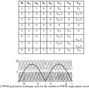
Table 1. Valid switching states of the proposed voltage source inverter output voltage
Fig.2 PWM generation technique used for the multilevel PWM single phase inverter.
The parameters of the modulation process are shown in Fig.2 and defined as following:
1) The modulation index is defined as:
Where Am is peak value of sinusoidal wave and Ac is the peak is the carrier peak-peak value. 2) The frequency modulation index:
Where the frequency of the carrier is wave and is the frequency of the sinusoidal wave.
3) The angle of displacement existing between the sinusoidal wave and the first positive carrier wave can be defined as following:
St Sa1 Sa2 Sb
1
Sb2 Van Vbn Vab
1 1 1 0 0 Vdc 0 Vdc
2 1 0 0 0 Vdc/2 0 Vdc/2
3 0 1 0 0 Vdc/2 0 Vdc/2
4 0 0 0 0 0 0 0
5 1 1 1 1 Vdc Vdc 0
6 1 0 1 1 Vdc/2 Vdc -
Vdc/2
7 0 1 1 1 Vdc/2 Vdc -
Vdc/2
II. PWM GENERATION USING XILINX FPGA
Fig.3 The block diagram of single phase PWM generator in XILINX FPGA
The upper and lower carrier waves (1800 Hz) are compared with the sinusoidal wave (50 Hz). In same time a pulse signal has frequency of (50 Hz) is generated and inverted to get its inverse pulse signal [8], [12].
There are only three control signals S6, S5 and S2 will be needed to derive, another three S3, S1, and S4 are simply generated in method of the logical inverse of S6, S5, and S2 respectively as shown in fig.4.
3.1 Sinusoidal Wave Generation
The schematic diagram of the sine wave consists of a memory Pointer unit and schematic block includes a VHDL program for sine wave data as shown in Fig.3. The VHDL program includes 19 sine wave data calculated at every 5° degrees, these data cover quarter cycle of sine wave 90° degrees [6-7].
As the modulation index depends on the modulation wave amplitude, the sine wave data can be changed to achieve the required modulation index and thus the required output voltage [13-15].
3.2 Carrier Wave Generation
An 8-bit up-down counter is clocked at 918 KHz to produce 1800Hz carrier frequency and VHDL program includes a simple addition process is also written and converted into schematic block (addition unit) to generate two types of carrier (upper and lower) waves. The main clock frequency is determined by the following formula:
Where is the main clock frequency, is the carrier (upper and lower) wave frequencies and n is the bit size of the up-down counter [9].
3.3 Pulse Signal 50Hz Generation
Two inverse pulse signals have same frequency (50Hz) need to be generated; their frequencies are similar to the sinusoidal wave and the output frequency [10]. Pointer unit consists of an 8 bit counter, some logic gates and VHDL program developed to store data in term of condition statements are the main structure of the pulse signal (50 Hz). These two signals have two functions, first as a switching signal for switches S4 and S2, second to involve with the resultant signals produced from comparators to generate the appropriate switching signals for switches S6, S3, S5 and S1 [11].
3.4 PWM Distribution Unit
This unit is used to distribute the PWM output pattern to the switches (S1, S2, S3, S4, S5 and S4). The distribution unit consists of a few logic gates (AND, OR, and NOT) deal with the three main signals produced from comparators and pulse signals 50 Hz generation unit to form the final PWM as shown in Fig.4.
III. SIMULATION RESULTS
The proposed capacitor clamped inverter is simulated using software package PSIM 6. The main components of proposed inverter are: C1=2200µF, C2=330µF, Co=18uF, Lo=1mH and Vo, rms=110V/60Hz. The capacitor voltage V2
equals 100V. The dc bus voltage is 200V. The triangular carrier frequency is 20 kHz. The figure 6.1 shows the simulated circuit diagram of the proposed inverter.
Fig.6 Simulation result for PWM generation.
VI. CONCLUSION
A single-phase voltage source inverter based on capacitor clamped configuration is proposed to provide a sinusoidal voltage to the output load. Three-level PWM scheme is used in the proposed inverter to reduce voltage harmonics on the ac side and reduce the voltage stress of the power semiconductors. The voltage stress of power devices is clamped to half the dc-link voltage.
Power switches in the one leg of inverter are operated at low switching frequency to generate two voltage levels on the voltage. Power switches in another leg of inverter are operated at high switching frequency to generate three voltage levels on the ac side voltage. Five voltage levels are achieved on the ac line output voltage.
REFERENCES
1. A. Nabae, I. Takahashi, and H. Akagi, 1981, “A new neutral point-clamped PWM inverter,” IEEE Transactions on Industry Applications, vol. 19,no. 5, pp. 518-523.
2. J. S. Lai and F. Z. Penf, 1996, “Multilevel converters – a new breed of power converters,” IEEE Transactions on Industry Applications, vol. 32, no. 3.
3. Jeyanthi Rebecca L., Dhanalakshmi V., Sharmila S., "Effect of the extract of Ulva sp on pathogenic microorganisms", Journal of Chemical and Pharmaceutical Research, ISSN : 0975 – 7384 , 4(11) (2012) pp.4875-4878.
4.M. Marchesoni, M. Mazzucchelli ans S. Tenconi, 1992, “A non conventional power converter for plasma stabilization,” in Proc. IEEE Power Electronics Specialist Conference, 1988, pp. 122-129.
5. J. Steinke, “Switching frequency optimal PWM control of a three level inverter,” IEEE Transactions on Power Electronics, vol. 7, no. 3, pp. 487-496.
6. Sharmila S., Rebecca L.J., Saduzzaman M., "Effect of plant extracts on the treatment of paint industry effluent", International Journal of Pharma and Bio Sciences, ISSN : 0975-6299, 4(3) (2013) pp.B678-B686.
7. L. M. Tolbert, F. Z. Peng and T. G. Habetler, 1999, “Multilevel PWM methods at low modulation indices,” in Proc. IEEE Applied Power Electronic Conference,
8. Y. Chen and B. T. Ooi, 1997, “Regulating and equalizing dc capacitor voltages in multilevel converters,” IEEE Transactions on Power Delivery, vol. 12, no. 2.
9. Shanthi B., Revathy C., Devi A.J.M., Subhashree, "Effect of iron deficiency on glycation of haemoglobin in nondiabetics", Journal of Clinical and Diagnostic Research, ISSN : 0973 - 709X, 7(1) (2013) pp.15-17.
10. T. A. Meynard and H. Foch, 1992, “Multilevel conversion: High voltage choppers and voltage source inverter,” in proc. IEEE Power Electronics Specialist Conference, pp. 397-403.
11. X. Yuan, H. Stemmler and I. Barbi, 1999, “Investigation on the clamping voltage self-balancing of the three-level capacitor clamping inverter,” in proc. IEEE Power Electronics Specialist Conference, pp. 1059- 1064.
13. X. Yuang; H. Stemmler and I. Barbi, 2001, “Self-balancing of the clamping-capacitor-voltages in the multilevel capacitor- clamping inverter under sub-harmonic PWM modulation,” IEEE Transactions on Power Electronics, vol. 16,
14. C. Turpin, L. Deprez, F. Forest, F. Richardeau, and T. A. Meynard, 2002, “A ZVS imbricated cell multilevel inverter with auxiliary resonant commutated poles,” IEEE Transactions on Power Electronics, vol. 17,no. 6, pp. 874 –882.
15. Menon R., Kiran C.M., "Concomitant presentation of alopecia areata in siblings: A rare occurrence", International Journal of Trichology, ISSN : 0974-7753, 4(2) (2012) pp.86-88.
16. B.R Lin, C.H Huang, September 2004 “analysis and implementation of a single phase capacitor –clamped inverter with simple structure,” IEE Proc-Electr.Power Appl, vol 151, no5, pp. 555-560.
17. S.-G. Lee, D.-W. Kang, Y.-H. Lee and D.-S. Hyun, 2001, “The carrier based PWM method for voltage balance of flying capacitor multilevel inverter,” in Proc. IEEE Power Electronics Specialists Conference, pp. 126 –131.
18. B Karthik, TVUK Kumar, Noise Removal Using Mixtures of Projected Gaussian Scale Mixtures, World Applied Sciences Journal, 29(8), pp 1039-1045, 2014.
19. Daimiwal, Nivedita; Sundhararajan, M; Shriram, Revati; , Non Invasive FNIR and FMRI system for Brain Mapping . 20. Daimiwal, Nivedita; Sundhararajan, M; , Functional MRI Study for Eye Blinking and Finger Tapping.
21. Shriram, Revati; Sundhararajan, M; Daimiwal, Nivedita; , Effect of change in intensity of infrared LED on a photoplethysmogramIEEE Communications and Signal Processing (ICCSP), 2014 International Conference on, PP 1064-1067,2014.
22. Kanniga, E; Srikanth, SMK; Sundhararajan, M; , Optimization Solution of Equal Dimension Boxes in Container Loading Problem using a Permutation Block AlgorithmIndian Journal of Science and Technology, V-7, I-S5,PP 22-26, 2014.