162
Multi Valued Logic Gate Implementation
Using MOSFET and CNTFET
1
A. Latha,
2S. Murugeswaran,
3Dr. G. Yamuna
1,2Research Scholar, Department of ECE, Annamalai University, Annamalai Nagar
3Professor and Head, Department of ECE, Annamalai University, Annamalai Nagar
1 [email protected], 2 [email protected] 3[email protected]
Abstract- In a VLSI circuit, around 70 percent of the area is focused on interconnection, 20 percent to security, and 10 percent to gadgets. The parallel reason is restricted due to interconnect which incorporates wide region on a VLSI chip. This issue is overcome by a heuristic technique for executing a multivalued reason, for example, a Ternary premise. Here low power dispersing MOSFET and CNTFET techniques for thinking is finished which is contained a course of action of ternary inverters and ternary NAND passages. Extensive HSPICE re-enactment result displays that the proposed CNTFET charts demonstrate an unrivalled change than the current MOSFET based plans in different execution estimations. The later utilization of the pseudo-N CNT FET MVL requires a more modest zone with a close actuating delay yet with more noteworthy PDP and static power. In this way, Ternary avocation can be used when just control is a basic concern and pseudo-ternary reason can be utilized when a transistor check and circuit a zone are fundamental. Future work will address the persevering idea of proposed MVL outlines and the impacts of chirality collection. Keywords: Different esteemed rationale, carbon nanotube field-impact transistor, ternary rationale, control postpone item.
1. INTRODUCTION
The power experience early automated plans brought by the scaling of CMOS progress has not obtained huge changes joined circuits. As CMOS approaches physical and imaginative inspirations driving control, new contraptions have been proposed to complete Nanoscale circuits, for instance, those in light of variously regarded procedure for considering (MVL). Generally, the mechanized figuring is performed on two regarded legitimization, i.e., there are only two possible characteristics (0 or 1, genuine or false) in the Boolean space. Specifically regarded bolster allows more than two levels of strategy for considering; utilization of ternary, quaternary, Penta for various applications. MVL perceives distinctive inspirations driving vitality over its parallel partner; for example, each wire can transmit more information, with the objective that the proportion of interconnections in the chip can be diminished, understanding a lower circuit multifaceted nature. In particular, CNTFETs have pulled in principal thought as a choice rather than silicon-based MOSFET for recognizing MVL doors as a result of its potential immaculate conditions, for instance, high flexibility of charge transporters.
2. MULTI VALUED LOGIC
Contrasting regarded commence allows more than two levels of reason; utilization of ternary, quaternary, Penta for various applications. MVL perceives distinctive inspirations driving energy over its parallel partner; for example, each wire can transmit more information, with the objective that the proportion of interconnections in the chip can be decreased, achieving a lower circuit multifaceted nature. Multi regard barrier replaces the standard Boolean depiction of components with either limitedly or unendingly extraordinary characteristics, for instance, a ternary method for considering.
K-163 regarded methodology for speculation system in
submicron VLSI is chip thickness. The chip region in submicron VLSI is all things considered controlled by the interconnections. In K regarded reason the proportion of interconnections can be reduced to1/log2 K in a relationship with a parallel methodology for considering. In case this effect can be connected with 2-dimensional geometry, the lessening degree pushes toward persuading the chance to be 1/ (log2 K) 2.
The total region of interconnections is controlled by the proportion of interconnections and their length. The interconnection length is in like route facilitated by the multifaceted idea of the interconnections, so certainly the usage of MVL is to a remarkable degree fundamental for conformist VLSI execution.
3. LOGIC LEVELS OF SWITCHING
Strategy for thinking passages set up the establishment debilitates for front line avocation. Conventional coordinated doors are use in current pushed contraptions. The multivalued strategy for thinking doors have not been systematized but rather ternary and quaternary entries are two generally utilized multivalued premise gateways depicted in creating.
Fig. 1 Logic levels of switching
4. TERNARY LOGIC
The most everything considered utilized exchanging circuit partitions today are two-respected or parallel. The electrical conditions controlling these exchanging circuit sections are additionally by and large two-respected or parallel. In any case, arranged circuits would now have the ability to oversee different respected signs and exchanging at speedy rather than twofold standards, particularly at information correspondence level due to the decreased interconnections and exchanging.
Use of multi respected technique for thinking (MVL) reduces the measure of signs attracted with the correspondence, expanding their data content. In such a way, an interconnection-restricted outline can be perceived with MVL like for the non-simultaneous circuits and in every practical sense indistinct execution than a standard coordinated game plan might be picked up. Among different sorts of MVL, the ternary technique for thinking gets more idea than others due to chop down interconnection cost estimation and a direct electronic circuit execution framework.
Ternary and quaternary circuits have been analyzed powerfully beginning late. Quaternary circuits have the down to earth favoured perspective that a four-respected flag can definitely be changed into a two-respected hail. In any case, in context of the running with contemplations, we feel that ternary circuits might be of more theoretical centrality than others:
Since 3 is the littlest radix higher than parallel, ternary capacities and circuits have less complex shape and development. They can be contemplated and talked about effortlessly, yet regardless they show the attributes of multivalued components.
As a proportion of the expense or intricacy of multi-esteemed circuits, the result of the radix and the quantity of signs has been proposed. Since 3 is the digit closest to e = 2.718, ternary circuits will be more practical as per this measure.
Whenever adjusted ternary rationale (1, 0, - 1) is utilized, a similar equipment might be utilized for expansion and for subtraction.
Since 3 isn't a basic intensity of 2, explore on ternary rationale may unveil outline procedures that are ignored in the investigation of parallel or quaternary rationale.
164
5. SCOPE OF MULTIVALUE LOGIC
Since cause impelled gadgets have been organized utilizing a twofold technique for thinking till date. Scientists have discovered the change in twofold avocation is sauntering, multifaceted and hard to get it. Since multivalued reason empowers more data to be pressed into a solitary digit inspectors have been overseeing multivalued strategy for thinking for a long time [1]-[3]. With the change of novel electronic contraptions and optical gadgets, it is straightforwardly conceivable to execute circuit for more convoluted premise structure [4]-[6].
Endless contraptions are fit for managing in excess of two techniques for thinking states yet they are at the exploratory stage. Some multivalued avocation structures, for example, a ternary and quaternary technique for thinking outlines have been made yet gainful utilize is yet to end up accessible.
Ternary strategy for thinking has several motivations behind eagerness requires twofold legitimization. Since it requires a colossal piece of the measure of digits to store any data than its twofold equal it is useful for constraint; the ternary gathering fragment isn't as much as twice as confounding as the consolidated structure.
Despite the way that their format rules of resistive stacked plans are beneficial in different parts, regardless they experience the detestable effects of sweeping static power utilization by virtue of the closeness of resistors. Emerged from the resistive stacked format the essential technique for thinking family displays some change. Nonetheless, specifically, the execution of pseudo strategy for thinking in the fundamental game-plan of premise portals like inverter, NAND and nor passage has appeared in this undertaking displays a beneficial outcome and separated and the above utilize.
TERNARY LOGIC IMPLEMENTATION IN MOSFET
CMOS coordinated innovation is thought to be the best decision for executing the ternary rationale circuits for the accompanying reasons:
CMOS multivalued circuits are depended upon to share three essential purposes of enthusiasm of CMOS matched circuits: zero static power scattering
in either stable state, a low-yield impedance in either state or transfer of uninvolved segments (resistors). Any multivalued flag can be transmitted through a CMOS transmission door.
In showing up diversely in connection to the PN-crossing point edge of a bipolar transistor, the MOS transistor's edge may easily be changed in the midst of fabricating, streamlining the endeavor of responding to an amazed information hail.
TERNARY INVERTER
For the ternary inverter the information sources are given as {0, 1, 2} and it yields the yield {2, 1, 0}. In light of its capacity to make {1} at the yield, ternary inverter is utilized as the essential building disappoint for the proposed SRAM cell and its CMOS execution depends upon the format in [2]. A high opposition transmission entryway is connected between the yield of a low-hindrance limit changed twofold inverter and 0.5Vs to pass within level voltage [1]. As expressed, the purpose of control voltage of transistors Q1 and Q2 is made piece of the supply voltage while transistors Q3 and Q4 were re-established with edge voltages as showed.
TERNARY NAND GATE
A general ternary NAND is a gadget with two wellsprings of information x1, x2 and three yields y0, y1, and y2 to such an extent, to the point that Yi=Ci(z) Where z= max (x1, x2) for i=0, 1 or 2. In the event that the yield is taken to be y0, y1, and y2 the contraption is hinted as the negative ternary NAND ( NTNAND ), a standard ternary NAND (ST-NAND ), or a positive ternary NAND ( PTNAND ), freely. Then again, if z= min (x1, x2) for i=0, 1 or 2, by then the general ternary NOR will fill in as general ternary NOR.
165 Fig 2 MOSFET – Ternary Inverter and NAND
gate
CNTFET
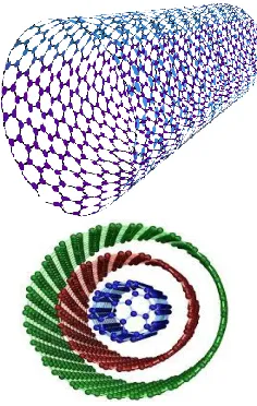
[image:4.612.74.275.135.419.2]cntfets use semiconducting single-divider cnts to amass electronic gadgets. alone divider cnt or SWCNT contains one barrel just and the reasonable accumulating procedure of this gadget makes it to an awesome degree engaging for decision instead of the present mosfet. a SWCNT can go about as either a conductor or a semiconductor subordinate upon the edge of the molecule blueprint along the tube. this is inferred as the chirality vector and is tended to by the whole number match nm a fundamental system to pick whether a cnt is metallic or semiconducting is to consider its reports nm the nanotube is metallic if nm or n −m 3i where I is a whole number. something remarkable the tube is semiconducting. the width of the cnt can be discovered in light of the running with going with.
Fig 3 CNTFET structure with four CNTs in channel
√ √
Where a0 = 0.142 nm is the interatomic expel between each carbon atom and its neighbor. Fig. 1 shows the schematic outline of CNTFET [14]– [16]. Like the regular silicon device, the CNTFET furthermore has four terminals. As showed up in above figure, undoped semiconducting nanotubes are put under the passage as channel locale, while strongly doped CNT parcels are set between the entryway and the source/drain to consider a low game plan resistance in the ON-state.
Fig 4 CNTFET – Single walled and Multiwalled Tubes
[image:4.612.382.500.444.630.2]166
TERNARY INVERTER
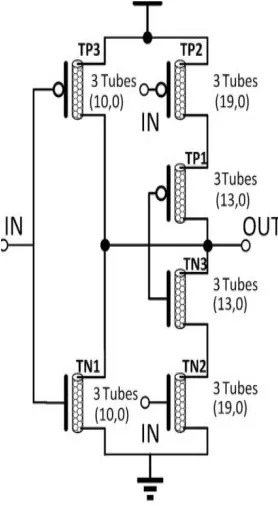
[image:5.612.101.240.392.645.2]A champion among the most by and large used justification design style is static proportional CMOS; the standard central purposes of the correlative framework are generosity, awesome execution, and low power usage with minimal static power scattering. A correlative CNTFET framework can moreover be used for ternary method of reasoning setup to achieve awesome execution, low power use, and to evade the use of broad resistors and lessening an area overhead. Fig 3.5 involves six CNTFETs. The chiralities of the CNTs used in T1, T2, and T3 are (19, 0), (10, 0), separates crosswise over of T1, T2, and T3 are 1.487, 0.783, and 1.018 nm, independently. Thusly, the edge voltages of T1, T2, and T3 are 0.289, 0.559, and 0.428 V, separately. The farthest point voltages of T5, T6, and T4 are −0.289, −0.559, and −0.428 V, independently. A champion among the most by and large used basis arrangement style is static proportional CMOS; the standard central purposes of the correlative layout are generosity, extraordinary execution, and low power use with minimal static power dispersal.
Fig 5 CNTFET – Ternary Inverter
A correlative CNTFET framework can similarly be used for ternary reason setup to achieve incredible execution, low power usage, and to avoid the use of
broad resistors and diminishing region overhead. Fig 5 involves six CNTFETs. The chiralities of the CNTs used in T1, T2, and T3 are (19, 0), (10, 0), and (13, 0), exclusively. From condition, the separations crosswise over of T1, T2, and T3 are 1.487, 0.783, and 1.018 nm, independently. Thusly, the edge voltages of T1, T2, and T3 are 0.289, 0.559, and 0.428 V, exclusively. The point of confinement voltages of T5, T6, and T4 are −0.289, −0.559, and −0.428 V, exclusively. addresses premise 1. Once the information voltage beats 0.6 V, both T5 and T6 are OFF, and T2 is ON to pull the yield voltage down to zero. The information voltage advance from high to low change resembles the low to high advancement.
CNTFET - TERNARY NAND
The circuits for the two-input ternary NAND is appeared in Fig 3.6 freely. Every last one of these two gateways contains ten CNTFETs, with three distinctive chiralities. They are in a general sense the same as their twofold CMOS associates, alongside the transistors of various edge voltages. In these two portals, like the STI circuit of Fig 3.5, the transistors with breadths of 1.487, 0.783, and 1.018 nm have edge voltages of 0.289, 0.559, and 0.428 V, autonomously, as set up utilizing limit voltage.
Fig 6 CNTFET – Ternary Nand
PSEUDO LOGIC- PSEUDO NCNTFET
[image:5.612.324.507.435.624.2]167 Pseudo-NMOS technique for thinking is a case of
[image:6.612.319.541.193.666.2]degree-ed premise which utilizes a grounded PMOS stack and a NMOS pull-down system that fathoms the legitimization work [5]. The standard perfect position of this technique for thinking is it utilizes just N+1 transistor fragments 2N transistors for static CMOS. In this support the exceptional yield voltage for any gateway is Vdd and the low yield voltage isn't 0volt. This outcomes in diminished commotion edge. The significant injury of this strategy for thinking is high static power use as there exists a brisk course among Vdd and ground through the PMOS transistor. With a specific genuine goal to make low yield voltage as pitiful as could be ordinary thinking about the current circumstance, the PMOS gadget ought to be surveyed by and large more modest than the NMOS pull-down contraptions. Be that as it may, to expand the speed especially when driving different unmistakable entryways the PMOS transistor measure must be made more prominent. Thusly there is dependably an exchange off between the parameters turmoil edge, static power dispersal and spread deferral.
Fig 7 Pseudo NCNTFET Ternary Inv
[image:6.612.70.214.386.580.2]Right when the information is justification 0, TN1, and TN2 in every one of the three frameworks [as appeared in Fig 7 are OFF . Since the yield is required to be technique for thinking 2 and the P-type CNTFET has a solid ability to exchange a high voltage, TP1 and TP2 in the pseudo-NCNTFET STI [see Fig 5] are both working in the huge triode region (or huge straight domain). The relative confirmations
of TP1 and TP2 are near nothing and unessential, as appeared in Fig 7. TP3 and TP2 in a correlative STI [see Fig 5] are both turned ON and work in the critical triode region. Thusly, the static power utilizations for each one of the three graphs are insignificant under this situation, as confirmed by the SPICE reenactment results.
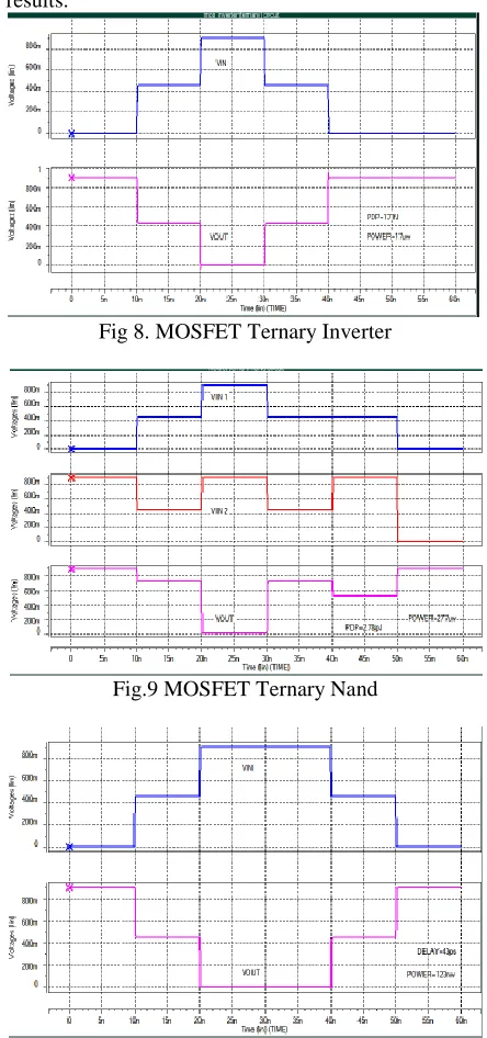
Fig 8. MOSFET Ternary Inverter
Fig.9 MOSFET Ternary Nand
168 Fig 11. CNTFET Ternary Nand
6. COMPARISON OF MOSFET and CNTFET
[image:7.612.304.554.185.390.2]Twofold and ternary technique for thinking entryway work inverter and NAND premise are portrayed out in both CMOS and CNTFET improvements. Power lessen is master in the ternary avocation with the unimportant expense of postponement and thusly the power surrender thing. Wandered from MOSFET control surrender thing CNTFET demonstrates more basic lessening in control which is appeared in the underneath table.
[image:7.612.64.295.409.705.2]Table: 1 Comparison of CMOS vs CNTFET for Inverter and NAND Gates
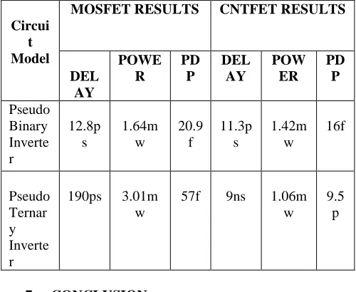
Table: 2 Comparison of Pseudo logic of MOSFET & CNTFET
7. CONCLUSION
In a VLSI circuit, around 70 percent of the area is focused on interconnection, 20 percent to security, and 10 percent to gadgets. The parallel reason is restricted due to interconnect which incorporates wide region on a VLSI chip. This issue is overcomed by a heuristic technique for executing a multivalued reason, for example, a Ternary premise. Here low power dispersing MOSFET and CNTFET techniques for thinking are finished which is contained a course of action of ternary inverters and ternary nand passages. Extensive HSPICE re-enactment result displays that the proposed CNTFET charts demonstrates an unrivalled change than the current MOSFET based plans in different execution estimations. The later utilization of the pseudo-NCNTFET MVL requires a more modest zone with a close actuating delay yet with more noteworthy PDP and static power. In this way, Ternary avocation can be used when just control is a basic concern and pseudo ternary reason can be utilized when transistor check and circuit a zone are fundamental. Future work will address the persevering idea of proposed MVL outlines and the impacts of chirality collection.
REFERENCES
[1] A.P Dhande, R.C Jaiswal and S.S Dudam, “Ternary Logic Simulator Using VHDL”, in SETIT; March 2007.
Circuit Model MOSFET RESULTS CNTFET RESULTS DEL AY PO WE R (uw ) PD P DEL AY PO WE R (uw) PD P (fJ) BINAR Y INVERT ER 24 ps
886 21.2 fJ
22ps 48 1
TERNA RY INVERT ER 9 ns
190 1.7 pJ
8ns 6 48
BINAR YNAND
60 ps
704 42.2 fJ
40ps 49 1.9
TERNA RY NAND
10 ns
277 2.7 pJ
9ns 8 72
Circui t Model
MOSFET RESULTS CNTFET RESULTS
DEL AY POWE R PD P DEL AY POW ER PD P Pseudo Binary Inverte r 12.8p s 1.64m w 20.9 f 11.3p s 1.42m w 16f Pseudo Ternar y Inverte r
190ps 3.01m w
57f 9ns 1.06m w
169 [2] International Technology Roadmap For
Semiconductors 2011 Edition.
[3] J. L. Huertas and J. M. Carmana, "Low power ternary C-MOS circuits," in Proc. 9th Int. Symp. Multiple-valued Logic, Bath, England, 1974, pp. 170-174; Oct 1984.
[4] J. Liang, L. Chen, J. Han, and F. Lombardi, “Design and reliability analysis of multiple valued logic gates ” in Proc.IEEE/ACM Int. Symp., Netherlands,2012, pp. 131–138.
[5] Jing hang Liang, Linbin Chen, “Design of MVL using Pseudo N-Type CNTFETs ,” in Proc. IEEECircuits, Devices Syst., vol. 137, no. 1, pp. 21–27, July 2014.
[6] KuldeepNiranjan, Sanjay Srivastava and Jaikaran Singh, MukeshTiwari ,”Comparative Study: MOSFET and CNTFET and the Effect of Length Modulation” , (IJRTE) ISSN: 2277-3878, Volume-1, Issue-4, October 2012.
[7] Kyung-Hoae Koo, Hoyeol Cho,PawanKapur, And Krishna C. Saraswat“Performance Comparisons Between Carbon Nanotubes, Optical, And Cu On-Chip Interconnect Applications”-IEEE Transactions On Electron Devices, Vol. 54, No. 12, December 2007. [8] S. Lin, Y. Kim, and F. Lombardi,
“CNTFET-based design of ternary logic gates and arithmetic circuits,” IEEE Trans. Nanotechnology., vol. 10, no. 2, pp. 217–225, Mar. 2011.
[9] TomazFelicijan and Steve B. Furber,” An Asynchronous Ternary Logic Signaling System,” IEEE Transactions On Very Large Scale Integration (VLSI) Systems, Vol. 11, No. 6, December 2003.
[10] Wu, X.W., Prosser, F.P. “CMOS ternary logic circuits,” Circuits, Devices and Systems, IEEE Proceedings, Volume: 137 Issue: 1, pp: 21 – 27, Feb 1990.
[11] S. Lin, Y. Kim, and F. Lombardi, "CNTFET-based arrangement of ternary reason entryways and number juggling circuits," IEEE Trans. Nanotechnology., vol. 10, no. 2, pp. 217– 225, Mar. 2011.
[12] TomazFelicijan and Steve B. Furber," An Asynchronous Ternary Logic Signaling System," IEEE Transactions On Very Large Scale Integration (VLSI) Systems, Vol. 11, No. 6, December 2003.