148
Parity Logic Based Content Addressable Memory for
Low Power Applications
1
S.Murugeswaran, 2A.Latha, 3Dr.G.Yamuna
1,2
Research Scholar, Department of ECE, Annamalai University, Annamalai Nagar
3Professor and Head, Department of ECE, Annamalai University, Annamalai Nagar 1[email protected], 2[email protected]3 [email protected]
Abstract- Content Addressable Memory (CAM) is a wonderful sort of memory which is especially useful in web crawlers and is altogether quicker. CAM structure made out of standard semiconductor memory SRAM with some extra hardware for making a gander at a move. CAM does the endeavor of restoring the regional district for a demanding word in a solitary clock cycle. CAM performs three sorts of activities particularly READ, WRITE and COMPARE undertaking. CAM sometimes does the READ and WRITE errand and in basic conditions, CAM is utilized for separating the Search word and the energy database and restoring the relating address zone inside a solitary clock cycle. A CAM mull over the information word in parallel for each piece and in this way devours higher power. Keeping in mind the end goal to diminish control, the regular CAM is changed in accordance with performing with additional extra consider piece a summary piece for every datum word. In that way, the time and power use can be lessened. In this undertaking, a correspondence bit based association is proposed in sensible anomaly to existing tally bit association with diminishing control. This decreases capacity to a promising way.
Keywords:CAM, Associative Memories, Low power, Parity bit, Low power ML, Memory Lookup Table
1. INTRODUCTION
Current impelled structures require the breaking point of anchoring and recovering an impressive proportion of data at high speeds. Recollections are circuits or structures that store robotized data in extensive aggregate. Semiconductor memory is an electronic information hoarding gadget which routinely utilized as PC memory finished on a semiconductor-based joined circuits. Semiconductor memory has the property of flighty access, which recommends that it requires a relative extent of theory to get to any memory domain, so information can be competently gotten to in any optional interest. A memory, which in single word time finds a sorting out region and looks at whatever is left of the word, has been called by one of these names as Content-Addressed
Memory (CAM) Data Addressed Memory (DAM), Content Associative Memory (CAM).
2.MEMORY ORGANIZATION
149
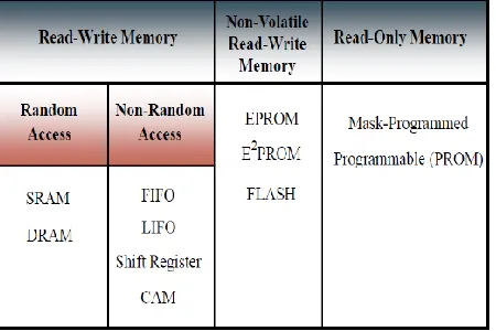
[image:2.612.73.298.346.496.2]the chip is to be gotten to. If the memory address incorporates M bits, the proportion of addresses on the chip is 2M, each containing an N bit word. Thusly, the degree of educational gathering endlessly in each chip is N2M bits. Past what many would consider conceivable is, for the most part, an intensity of two: 2, 4, 8, 16, 32, 64, 128, 256 and 512 and surveyed in KB-bits, MB-bits, GB-bits or TB-GB-bits, et cetera. Starting best case scenario semiconductor memory chips hold a couple of GB of data, yet higher cutoff memory is constantly being made. Semiconductor memories are totally depicted into three classes which are appeared in underneath a table
Fig. 1 Memory Classification
Read Write Memories are ordered into two classes as
1. Random Access Memories
2. Non – Random Access Memories.
Sporadic access memory (RAM) is a non-restrictive term that recommends both SRAM and DRAM or, truly, any sort of memory where you can valiantly (thoughtlessly) discover the chance to stay data. Non-Random Access Memories is what's more named as "Serial Access Memories". These are fairly memory in which data is gotten to consistently and the perfect open portal for finding
the opportunity to depend on the region of the data required. In a multiport memory, this term suggests that bit of the contraption that is related to the serial-discover the chance to port and its related limits. Content Addressable Memory is one such Serial Access Memories which get to the data in a development and the most extreme contraption encounters all information up to the point it is endeavoring to look at or make. These are to some degree memory which is used for permanent accumulating, not in the least like the Random access memories which are used as the concise Storage.
3. CONTENT ADDRESSABLE MEMORY
Content Addressable Memories (CAMs) are hardware web crawlers that are altogether speedier than algorithmic procedures to look for genuine applications. CAMs are made out of customary Semiconductor memory especially SRAM with included connection equipment that engages an interesting movement to complete in a singular clock cycle. CAM works in three modes
READ
WRITE
COMPARE
4. CAM ARCHITECTURE
150
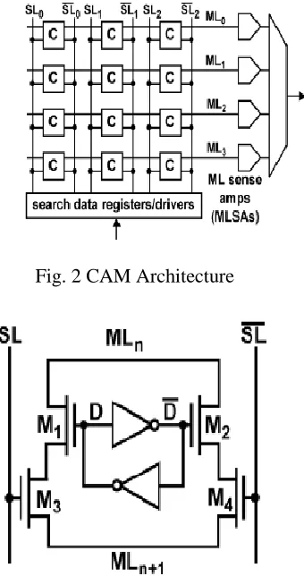
[image:3.612.110.280.368.690.2]stacking the pursuit information word into the demand information registers taken after by pre-charging all match lines high, putting them all by chance in the match state. Next, the demand line drivers pass on the intriguing word onto the differential pursue lines, and every CAM center cell looks set away piece against the bit on its relating search for lines. Match lines on which all bits orchestrate to stay in the pre-charged-high state. Match lines that have no shy of what one piece that misses, release to ground. The MLSA by then sees whether its match line has an arranging condition or miss Condition. At long last, the encoder maps the match line of the sorting out an area to its encoded address.
Fig. 2 CAM Architecture
Fig. 3 10T - NOR based CAM CORE CELL
5. CHALLENGES IN CAM DESIGN
Full parallel interest movement prompts fundamental troubles in plotting a low-control system for quick high-confine CAMs:
Power hungry nature because of the high exchanging movement of SL and the ML.
A tremendous flood on momentum (i.e., top ebb and flow) happens toward the start of the hunt activity because of the simultaneous assessment of the ML may cause a genuine IR drop on the power network, consequently influencing the operational dependability of the chip.
As a result, numerous efforts have been put forth to reduce both the peak and the total dynamic power consumption of the CAMs.
6. ADVANTAGES OF CAM
A Critical good position that CAM offers are quick handiness. Distinctive inclinations are
Data Storage and recuperation limits.
Programming unwinding in the context of the likelihood of expelling the condition of information in memory and wide utilization of substance tending to and requested recovery.
Programming disentangling in the context of the likelihood of expelling the situation of information in memory and wide utilization of substance tending to and requested recovery.
151
7. COUNT BIT BASED CAM
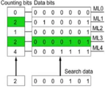
[image:4.612.332.509.136.285.2]All things considered, a CAM has three action modes: READ, WRITE, and COMPARE, among which "Consider" is the rule undertaking as CAM now and again scrutinizes or forms. It starts a glance at errand by stacking an n-bit input look for word into the request data enroll. The request data are then conveyed into the memory banks through n sets of corresponding chase lines SL and ~SLs particularly differentiated and the majority of the set away words using relationship circuits. Each set away word has an ML that is shared between its bits to pass on the examination result. A territory of the planned word will be recognized by a yield encoder, as showed up in Figure 1. In the midst of a pre-charge mastermind, the MLS is held at ground voltage level while both SL and ~SLs are at VDD. In the midst of appraisal sort out, corresponding request data is imparted to the SL and ~SL. Exactly when confuse occurs in any CAM cell (for example at the vital cell of the line D= "1"; ~D="0"; SL ="1"; ~SL="0"), transistor P3 and P4 will be turned on, empowering the ML to a higher voltage level. A sense intensifier (MLSA) is used to recognize the voltage change on the ML and opens up it to a full CMOS voltage yield. In the occasion that confuses happens to none of the cells on a line, no stimulate way will be molded and the voltage on the ML will remain unaltered, demonstrating a match.
Fig 4. Conceptual View of Pre-computation based CAM design
Since each and every open word in the CAMs is taken a gander at in parallel, a result can be gotten in a singular clock cycle. In this way, CAMs are speedier than other hardware and programming based chase systems. They are in this way supported in high-throughput applications, for instance, sort out switches and data blowers. In any case, the full parallel interest action prompts fundamental troubles in arranging a low-control system for quick high-confine CAMs. The power-hungry nature on account of the high trading development of the ML and the SL and a goliath surgeon stream (i.e., peak force) occurs toward the beginning of the request errand as a result of the concurrent appraisal of the SL may cause a bona fide IR drop on the power lattice, thusly affecting the operational steadfastness of the chip. Along these lines, different undertakings have been progressed to reduce both the apex and the total exceptional power usage of the CAMs.
PRE COMPUTATION SCHEME DESIGN
152
[image:5.612.85.285.263.546.2]veritable examination. These additional bits are gotten from the information bits and are utilized as the fundamental examination orchestrate model, in figure 4 number of "1" in the set away words are fused and kept the Counting bits part. Precisely when an intrigue
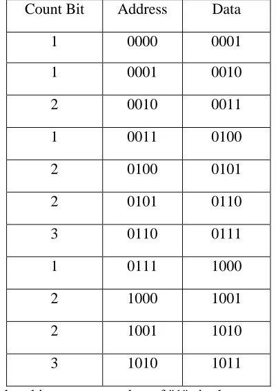
Table 1. Memory Lookup table
Count Bit Address Data
1 0000 0001
1 0001 0010
2 0010 0011
1 0011 0100
2 0100 0101
2 0101 0110
3 0110 0111
1 0111 1000
2 1000 1001
2 1001 1010
3 1010 1011
2 1011 1100
Undertaking begins, a number of "1"s in the demand word is tallied and anchored to the zone on the left of the figure. These additional data are looked at those that have a similar number of "1"s (e.g., the second and the fourth) are turned on in the second distinctive stage for development association. This plan decreases a lot of intensity required for information association, precisely. The rule plan thought is to utilize extra silicon space and pursue deferral to diminish significance utilize.
The starting at now said pre-tally and all other existing formats shares one identical property. The ML sense intensifier in a general sense needs to see the arranged ML and the 1-baffle ML. This makes CAM plots at some point or another face challenges since the driving idea of the single turned-on way are getting weaker after each procedure age while the spillage is getting more grounded. This issue is generally intimated as Ion/I off.
For example, in figure 4 number of "1" in the set away words are incorporated and kept the Counting bits part. Exactly when an interest however in actuality has an alternate working rule.
Undertaking starts, number of "1"s in the request word is counted and secured to the area on the left of figure. These extra information are taken a gander at sole those that have a comparable number of "1"s (e.g., the second and the fourth) are turned on in the second distinguishing stage for advance connection. This arrangement diminishes a great deal of power required for data connection, accurately. The guideline plan thought is to use additional silicon domain and chase deferral to decrease imperativeness use.
153
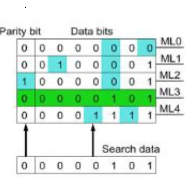
PARITY BIT BASED CAM DESIGN
A flexible assistant piece is acquainted with help the pursuit speed of the CAM at the expense of less than 1% region overhead and power utilization. This recently presented helper bit initially is like the current Pre-calculation plots however in actuality has an alternate working rule.
[image:6.612.329.547.149.565.2].
Fig 5. Conceptual View of Parity based CAM design
By virtue of an organized in the data parcel (e.g., ML3), the equity bits of the chase and the
set away word is the same, in this way the general word reestablishes a match. Exactly when 1 befuddle occurs in the data piece (e.g., ML2), amounts of "1"s in the set away and look word must be changed by 1. Along these lines,
the relating fairness bits are unprecedented. Thusly now we have two muddles (one from the
balance bit and one from the data bits). If there are two puzzles in the data divide (e.g., ML0, ML1 or ML4), the correspondence bits are the
same and as a rule it has two disorders. With
more bungles, we can overlook these cases as
Table 2 Parity Bit Look-up Table they are not urgent. The fairness bit based CAM design is showed up in above figure involving the primary data area and an extra one-piece partition, got from the genuine data bits. Procedure is to get only the balance bit, i.e., odd or fundamentally number of "1"s. The got balance bit is put particularly to the relating word and ML. In this way the new outline has indistinct interface from the regular CAM.
Parity Bit Data
0 1111
1 0010
0 0011
0 0000
0 0101
0 0110
1 0111
1 1000
0 1001
0 1010
1 1011
[image:6.612.76.263.272.453.2]154
8. RESULTS AND DISCUSSIONS
The Memory circuits are conveyed through Verilog HDL utilizing XILINX ISE Simulator (Version 9.2i). Read, Write and Compare errands for both the methodologies are replicated near to their capacity examination. Power examination is done utilizing XILINX Power analyzer contraption.
[image:7.612.322.564.135.298.2]Fig. 6 Write Operation of CAM
[image:7.612.72.307.277.445.2]Fig 7 Read Operation of CAM
Fig 8 Compare Operation of CAM
CAM circuits are created for both scrutinized, form and dissect undertaking for both pre-computation based and fairness based framework techniques.
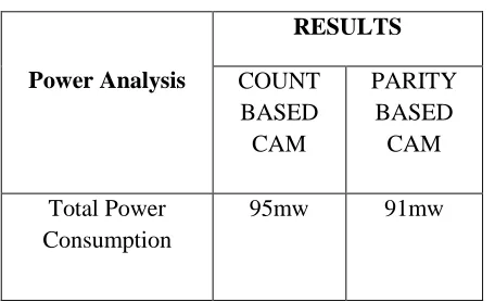
Table 3 Power Consumption in
Count and parity based technique.
From Results, we separated that Parity based CAM circuits eat up less power when contrasted with the tally bit based pre-calculation CAM. Additionally, the inquiry speed is likewise better in the equality based CAM outline. From the above power correlation table, unmistakably Content Addressable Memory rationale executed in light of Parity bit rationale devours lesser power when contrasted with the Content Addressable Memory rationale actualized with the regular pre-calculation based outline of rationale usage utilizing Count bit technique
Power Analysis
RESULTS
COUNT BASED CAM
PARITY BASED
CAM
Total Power Consumption
[image:7.612.66.294.503.642.2]155
9. CONCLUSION
Resolute nature of a thing portrays the limit of a structure or part to play out its required limits under communicated conditions for a foreordained time allotment. Nature of thing is picked in perspective of steadfast nature of the chip. For an Integrated Circuit (IC), as a fundamental thing specific under the present mighty advancement scaling, unflinching quality has constantly been to a great degree troublesome and over the top to evaluate, and to achieve in driving edge development. In this paper, a novel low-control and particularly trustworthy Content Addressable Memory method of reasoning have been proposed to extend the chase speed and decrease the power use in the midst of examining action. In this way, two distinct techniques are created to recognize the reduction in control usage. CAM consumes higher power in the midst of taking a gander at the cycle and from this time forward essential measures are taken to decrease the power in considering a cycle. Basically, the current conventional CAM takes after the technique of pre-estimation system for including an extra check bit which stores the amount of count-based relationship and from this time forward the new methodology proposed depends. From the above power correlation table, it is obviously demonstrated that equality based substance addressable memory expends less power when contrasted with the regular plan of tally based substance addressable memory. From this time forward the new methodology proposed relies upon the balance bit based examination which helps in charge diminish.
REFERENCES
[1] Arsovski, I. in like manner, Sheikholeslami, A. "An overwhelm subordinate power errand strategy for sort out line distinguishing in content-addressable recollections," IEEE J.
Strong State Circuits, vol. 38, no. 11, pp. 1958– 1966, Nov. 2003.
[2] Baeg, S. "Low power ternary substance addressable memory setup utilizing an appropriated sort out line," IEEE Trans. Circuits Syst. I, Reg. Papers, vol. 55, no. 6, pp. 1485– 1494, Jul. 2008.
[3] Do, A. T. Chen, S. S. Kong, Z. H. furthermore, Yeo, K. S. "A low-control CAM with fit power and put off exchange off," in Proc. IEEE Int. Symp. Circuits Syst. (ISCAS), 2011, pp. 2573– 2576.
[4] Mohan, N. Fung, W. Wright, D. additionally, Sachdev, M. "A low-control ternary CAM with positive-input encourage line sense speakers," IEEE Trans. Circuits Syst. I, Reg. Papers, vol. 56, no. 3, pp. 566– 573, Mar. 2009.
[5] Mohan, N. additionally, Sachdev, M. "Low-spillage collecting cells for ternary substance addressable recollections," IEEE Trans. Far reaching Scale Integr. (VLSI) Syst., vol. 17, no. 5, pp. 604– 612, May 2009.
[6] Pagiamtzis, K. moreover, Sheikholeslami, A. "A low-control content-addressable memory (CAM) utilizing pipelined distinctive leveled search for plan," IEEE J. Strong State Circuits, vol. 39, no. 9, pp. 1512– 1519, Sep. 2004.
[7] Pagiamtzis, K. besides, Sheikholeslami, A. "Content-addressable memory (CAM) circuits and structures: An instructional exercise and review," IEEE J. Strong State Circuits, vol. 41, no. 3, pp. 712– 727, Mar. 2006.