A Small-Signal Analysis Based Thermal Noise Modeling Method
for RF SOI MOSFETs
Xiang Wang, Yu Ping Huang, Jun Liu*, and Jie Wang
Abstract—We investigate thermal noise mechanisms and present analytical expressions of the noise power spectral density at high frequencies (HF) in Silicon-on-insulator (SOI) MOSFETs. The developed HF noise model of RF T-gate body contact (TB) SOI MOSFET for 0.13-µm SOI CMOS technology accounts for the mechanisms of 1) channel thermal noise; 2) induced gate noise; 3) substrate resistance noise and 4) gate resistance thermal noise. The extraction method of modeling parameter utilized by
Y-parameter analysis on the proposed small-signal equivalent circuit is demonstrated in this paper. Excellent agreement between simulated and measured noise data is obtained at different temperatures.
1. INTRODUCTION
SOI technology has been considered as a potential technology for low-power microwave circuits due to its excellent RF performance such as gain, speed, and cutoff frequency (fT) [1]. It is prerequisite for the
application of modern SOI technologies in RF circuits to better understand noise mechanisms [2–5]. For the applications in low noise CMOS RF circuits such as low noise amplifier (LNA), accurate modeling of noise is quite important. In the past decade, HF noise characterization and modeling for bulk and floating body SOI MOSFETs has been widely studied [6–15], and some modeling methods have been proposed. In [16], the authors proposed a channel segmentation model for accurate channel noise by several independent MOS model. In [17], the author presented a physical understanding of both intrinsic and extrinsic noise mechanisms in a MOSFET [18], a simple analytical model for the thermal channel noise of deep-submicron MOS transistors including hot carrier effects. However, the HF noise model of TB SOI MOSFET is rarely presented and discussed. Accurate physical-based noise model is needed to shorten the design cycle.
To HF noise modeling, the small signal circuit parameters and noise sources play important roles. In Section 3, we perform an extensive study of the noise mechanisms at high frequencies. The small signal equivalent circuit and parameter extraction techniques for TB SOI MOSFET are presented. In Section 4, we model the total drain-current noise, the gate-current noise, their cross-correlation and the four noise parameters. Finally, experimental verifications of the derived noise model are given at different temperatures.
2. PROPOSED DEVICE STRUCTURE
To suppress floating body effect (FBE), body contacts with different structures have been proposed. In this paper, multi-finger PD SOI nMOSFETs with TB structure are investigated. For a TB device,
P+ implantation is performed to form the P+ body contact area. At one end of the T-type gate, a
P+ injection region is connected to the P-type body region. Because of the P+ body contact area is connected with the ground, the hole produced by the impact ionization can be released from the body region in order to eliminate the Kink effect. The layout of TB SOI nMOSFET is shown in Fig. 1.
Received 6 March 2017, Accepted 24 May 2017, Scheduled 2 June 2017 * Corresponding author: Jun Liu ([email protected]).
P+ implantation
Figure 1. Top view of the proposed TB SOI nMOSFET structure.
3. MODEL PARAMETER EXTRACTION
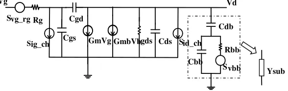
A simplified small-signal equivalent circuit with the associated noise sources of TB SOI MOSFET is proposed in Fig. 2. Rg, Rs,Rdare gate resistance, source resistance, and drain resistance, respectively.
Gds is the ac drain conductance andGm the ac transconductance. Cds, Cgs andCgdare drain-to-source
capacitance, gate-to-source capacitance and gate-to-drain capacitance, respectively.
Rbb Cdb
Cbb gds
GmVg Cgd
Cgs Rg
Vg Vd
Cds Svg_rg
Svbb Sid_ch
Sig_ch GmbVb
Ysub
Figure 2. SOI MOSFET simplified small-signal equivalent circuit including the relevant noise sources.
In order to verify the accuracy of the proposed noise model at different temperatures, on-wafer two-port high-frequency scattering parameters (S parameters) and noise figure (NF) under ultra-low temperatures are measured from 1 to 20 GHz with a step size of 1 GHz by Universit´e de Bordeaux. We use an accurate parameter-extraction approach [19] to get Y-parameters from deembedded S-parameters. The higher order terms of ωRXCX are too small to be neglected in the
measurement frequency range. Y-parameter analysis on the proposed small-signal equivalent circuit can be approximated as follows:
Y11 = I1 V1
V2=0
≈ω2(Cgd+Cgs)2Rg+jω(Cgd+Cgs) (1)
Y12 = I1 V2
V1=0
≈ −ω2Cgd(Cgd+Cgs)Rg−jωCgd (2)
Y21 = I2 V1
V2=0
≈Gm−jω(Cgd+Cgs)RgGm (3)
Y22 = I2 V2
V1=0
≈Ysub+Gds+jω(Cgd+Cgs) +Gmb
Vbs
Vds
(4)
Vbs
Vds
= Ysub
(1−jωRbbCbb)Rbb
1 +ω2R2
bbCbb2
For the extraction of substrate components, Ysub can be defined as follows:
Ysub= ω
2R
bbCdb2 +jωCdb+jω3RbbCdbCbb(Cdb+Cbb)
1 +ω2R2
bb(Cdb+Cbb)
2 (6)
All the components of the equivalent circuit can be extracted by theY-parameter analysis. Gm,
Gds, Rg, Cgd, Cgs and Cds are expressed as.
Gm ≈ Re [Y21]|ω2=0 (7)
Gds ≈ Re [Y22]|ω2=0 (8)
Rg ≈
Re [Y11]
Im [Y11]2
(9)
Cgd ≈ −
Im [Y12]
ω (10)
Cgs ≈
Im [Y11] + Im [Y12]
ω (11)
Cds =
Im (Y22)
ω −Gds (12)
Rbb,Cbb and Cdb can be derived as [13]. In this paper, we simplify the extraction that Rbb is obtained
from the slope of the relationship forω2/Re[Ysub] versus ω2 as follows:
ω2
Re [Ysub]
=ω2Rbb+
1
RbbCdb2
(13)
Cdb is extracted from (13) as follows:
Cdb=
ω2Rbb
Re [Ysub]−ω
2 R2bb
−1 2
(14)
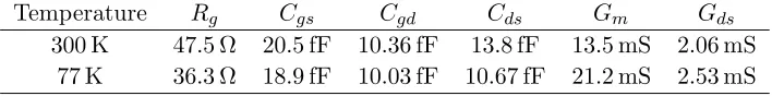
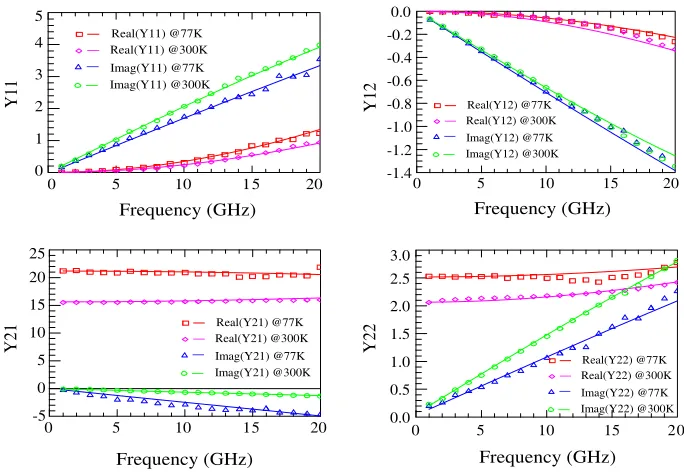
In this paper, the parameter-extraction technique is performed using multi-finger PD SOI nMOSFETs with TB structure of the channel length L = 0.13µm, channel width W = 5µm and number of fingers N = 4 at a biasing condition of Vgs = 0.8 V, Vds = 1.2 V. The cryogenic DC performance
and small signal AC performance of PD SOI nMOSFETs with TB structure can refer to [20, 21]. As shown in Fig. 3, the simulated Y-parameters are found to agree well with the measuredY-parameters which indicates that the proposed small-signal equivalent circuit model can describe linear two-port characteristics commendably. The small signal parameters extracted at 300 K and 77 K are enumerated in Table 1. The decrease in the gate resistance Rg at 77 K is due to lower poly/silicide resistances at
low temperatures. The capacitances are almost invariant with temperature. Gm and Gds increase with
decrease in temperature, largely due to increase in the effective mobility.
Table 1. Values of the extracted model parameters biased at Vgs = 0.8 V, Vds = 1.2 V, at 300 K and
77 K.
Temperature Rg Cgs Cgd Cds Gm Gds
300 K 47.5 Ω 20.5 fF 10.36 fF 13.8 fF 13.5 mS 2.06 mS 77 K 36.3 Ω 18.9 fF 10.03 fF 10.67 fF 21.2 mS 2.53 mS
4. HIGH-FREQUENCY NOISE MODEL
0 5 10 15 20 0
1 2 3 4 5
Frequency (GHz)
Y11
Real(Y11) @77K Real(Y11) @300K Imag(Y11) @77K Imag(Y11) @300K
0 5 10 15 20 -1.4
-1.2 -1.0 -0.8 -0.6 -0.4 -0.2 0.0
Real(Y12) @77K Real(Y12) @300K Imag(Y12) @77K Imag(Y12) @300K
Frequency (GHz)
Y12
0 5 10 15 20 -5
0 5 10 15 20 25
Real(Y21) @77K Real(Y21) @300K Imag(Y21) @77K Imag(Y21) @300K
Frequency (GHz)
Y21
0 5 10 15 20 0.0
0.5 1.0 1.5 2.0 2.5 3.0
Frequency (GHz)
Y22
Real(Y22) @77K Real(Y22) @300K Imag(Y22) @77K Imag(Y22) @300K
Figure 3. Extracted (symbols) and simulated (lines)Y-parameters versus frequency.
Sigid∗ are required, and the noise performance of any noisy two-port network can be represented by
Eq. (15).
N F =N Fmin+Rn
Gs|Ys−Yopt|
2 (15)
N F is the noise figure, N Fmin the minimum noise figure, Rn the equivalent noise resistance, Yopt (=
Gopt+j∗Bopt) the optimum source admittance that results inN Fmin, and Ys (=Gs+j∗Bs = 50) the
source admittance.
4.1. Channel Thermal Noise
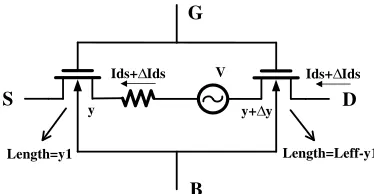
The channel thermal noise induced by the random motion of the carriers in the inversion channel of the MOS transistor is the main contribution to the drain current noise power spectral density (PSD) [22]. The channel thermal noise model is developed based on Tsividis’ method [23], and the linear part of channel is divided into small sections of length Δy as shown in Fig. 4. However, Tsividis cannot consider the impact of channel length modulation (CLM), velocity saturation effect (VSE) and hot carrier effect (HCE) [24–26]. In addition, experimental results indicate that GCR (gradual channal region) significantly contribute to the channel thermal noise [27]. Fig. 5 shows a detailed schematic indicating the partition in the GCR and velocity saturation region (VSR), which is used in the noise analysis. The negligible contribution from the VSR can be attributed to the fact that carriers travel at constant velocity and therefore are insensitive to channel voltage random fluctuations [28]. With consideration of these effects [29], the channel thermal noise can be derived,
Sid ch=
4kT IDS
⎡ ⎢ ⎢ ⎣
W Leffμeff
1 + VDSeff
EcLeff ⎤ ⎥ ⎥ ⎦ 2
VDSeff
0
1 + VDSeff
EcLeff
×QI(Vy)
2
dVy (16)
QI(Vy) = Cox (VGT −αVy) is the inversion layer charge density. Cox is the gate capacitance per unit
area. kis Boltzmann’s constant. αis the bulk charge effect coefficient,μeff the effective mobility of the
carrier,Leff =L−dLthe length of the gradual channel region, andVDSeff the drain bias smoothening
function, which are obtained from BSIMSOI4. Ey is the lateral electric field andEc the critical electric
Length=y1 Length=Leff-y1
y y+Δy
G
S D
B
Ids+ΔIds V Ids+ΔIds
Figure 4. Thevenin equivalent circuit.
N+ Buried oxide P Source Gate Drain Ts i TB o x N+ Substrate GCR VSR L' Lsat
Figure 5. Cross-sectional view of SOI MOSFETs indicating the GCR and the VSR.
The channel thermal noise can be derived as follow:
Sid ch= 4kT
W LeffμeffC
ox × ⎛ ⎜ ⎜ ⎝
VGT2 −αVGTVDSeff +
α2
3 V
2
DSeff
VGT −α
2VDSeff
⎞ ⎟ ⎟
⎠ (17)
4.2. Induced Gate Noise
The channel thermal noise is coupled to the gate terminal through the gate capacitance, resulting in the induced gate noise. The magnitude of this noise is directly proportional to the frequency as the earlier work by van der Ziel [30], and the induced gate noise was modeled for a MOSFET by Shoji [31] that treated the channel as an active distributed RC transmission line. Based on [13, 30], we consider the gradual channel approximation, and the induced gate noise spectral density can be obtained,
Sig ch=ω2W2C
2
ox
L2eff IDS2
4kT IDS ⎡⎢ ⎢ ⎣ W Leffμeff
1 + VDSeff
EcLeff ⎤ ⎥ ⎥ ⎦ 2 ×
VDSeff
0
1 +Ey
Ec
QI2[Vas−Vy]2dVy (18)
WithVas=VDSeff +EcL1eff
V2
DSeff
2
−1 +VEDSeff
cLeff
1
2VGTVDSeff−α6VDS2 eff VGT−α2VDSeff
.
By integrating Eq. (18) over the whole channel, the induced gate noise spectral density is given as,
Sig ch=
4kT ω2W4Cox4μ2eff
I3 DS ⎛ ⎜ ⎜ ⎝ 1
1 + VDSeff
EcLeff ⎞ ⎟ ⎟ ⎠× α2 5 V 5
DSeff −
α
2 (αVas+VGT)V
4
DSeff
+1 3
α2Vas2 + 4αVasVGT +VGT2
VDS3 eff −VasVGT (αVas+VGT)VDS2 eff +VGT2 Vas2VDSeff
(19)
4.3. Substrate Resistance Noise
According Jindal’s original analysis [32], the thermal voltage fluctuations across the total distributed substrate resistance Rbb induces a fluctuating substrate potential, and these random variations are coupled to the FET channel. Based on Nyquist’s assertion of thermal noise [33], the noise voltage spectrum can be adequately described by Equation (15) and coupled to the channel through the back-gate (substrate) transconductanceGmb.
Svbb = 4kT Rbb (20)
Sid sub = 4kT Rbb× G
2
mb
1 +ω2C2
bR2bb
The thermal noise generated in the substrate network is coupled to the gate terminal through the gate–bulk capacitance Cgb, resulting in gate-current noise Sig sub. Due to the small Cgb, Sig sub can
be negligible. Effective substrate capacitance Cb is approximately equal to the channel-substrate series
capacitance. Due to the thick buried oxide (BOX) in SOI MOSFET,Cb is approximately equal toCdb.
The noise contribution from the substrate resistance can be reduced by using a high resistive substrate (Rbb→ ∞) or a “metallic” substrate (Rbb→0).
4.4. Gate Resistance Thermal Noise
When the device transconductance approximates the conductance of the resistive gate, the resistive gate becomes important and can be a significant contributor to noise. Thornber [34] first proposed a solution to this problem for a simple gate geometry. In fact, typical IC layouts are far more complex, so Jindal developed new formulation with many effects [35]. Like any other AC signal, the voltage noise across the gate resistance can be amplified to the drain through transconductance Gm. An additional
drain current noise can be derived as Eq. (22). At high frequency, the gate-current noise due to the voltage noise across the gate resistance cannot be recognized [35] and can be obtained as Eq. (23).
Sid Rg = 4kT RgG2m (22)
Sig Rg = 4kT Rgω2Cgg2 (23)
4.5. Correlation between Drain-Current Noise and Gate-Current Noise
Since the noise sources of the channel current noise Sid ch and channel-induced gate noise Sig ch are
both from the channel, Sid chand Sig ch are correlated, and this noise correlation can be given by,
Sigid∗ ch = jωW Cox
Leff IDS
4kT IDS
⎡⎢ ⎢ ⎣
W Leffμeff
1 + VDSeff
EcLeff ⎤ ⎥ ⎥ ⎦ 2
×
VDSeff
0
1 +Ey
Ec
QI2[Vas−Vy]2dVy(24)
Sigid∗ ch =
4kT ωW3Cox3μ2eff
LeffIDS3
⎛ ⎜ ⎜
⎝ 1
1 + VDSeff
EcLeff ⎞ ⎟ ⎟ ⎠×
−1
4V
4
DSeff +
α
3 (αVas+ 2VGT)V
3
DSeff
−(Vgs−Vth)
2 (2αVas+Vgs−Vth)V
2
DSeff + (Vgs−Vth)2Vas(αVas+VGT)VDSeff
(25)
The contributions of the gate resistance to drain current and gate current noise are correlated, and the correlation is expressed as [36]:
Sigid∗ Rg =j4kT ωCggRgGm (26)
Based on the calculated noise sources, we can summarize the total drain-current noise Sid, total
gate-current noiseSig and their cross-correlation Sigid∗.
Sid = Sid ch+Sid rg+Sid sub (27)
Sig = Sig ch+Sig rg (28)
Sigid∗ = Sigid∗ch+Sigid∗rg (29)
In the end, the four noise parameters can be modeled from the noise power spectral density [37].
Rn = Sid
4kT|Y21|2
(30)
Bopt = −Bcor= S
igid∗Re [Y21]
4kT Rn|Y21|2
−Im [Y11] (31)
Gopt =
|Yopt|2−Bopt2
1 2
=
Sig
4kT Rn − |Y11|
2+ 2 (Re [
Y11]Gcor+ Im [Y11]Bcor)−Bopt2
1 2
Gcor = Re [Y11] +Sigid
∗Im [Y21]
4kT Rn|Y21|2
(33)
Fmin = 1 + 2Rn(Yopt+Ycor) = 1 + 2Rn(Gopt+Gcor) (34)
Extracted total drain-current noiseSid, total gate-current noiseSig and their cross-correlationSigid∗
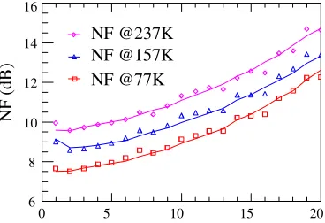
versus frequency for different temperatures are shown in Fig. 6. A positive temperature coefficient of the NF extracted in Eq. (15) versus temperature can be seen in Fig. 7. The good fitting results prove the accuracy of the proposed noise model.
0 5 10 15 20 0.0
0.5 1.0 1.5 2.0 2.5
Dr
ain
Curr
en
t
N
o
ise(10
-2
1A 2/H
z)
Sid @237K Sid @157K Sid @77K
(a)
0 5 10 15 20 0
2 4 6 8
Sig @237K
G
ate Cur
rent
Nois
e(
1
0
-2
1A 2/H
z)
Sig @157K Sig @77K
Frequency (GHz) (b)
0 5 10 15 20
0 1 2 3 4
Sigid*@237K Sigid*@157K Sigid*@77K
(c)
Correlation (10
-2
1A 2/H
z)
Frequency (GHz)
Figure 6. Extracted noise power spectral density versus frequency at 77 K, 157 K and 237 K. (a) Total drain-current noise, (b) total gate-current noise Sig, (c) cross-correlation.
0 5 10 15 20 6
8 10 12 14 16
NF @237K NF @157K NF @77K
NF
(
d
B
)
5. CONCLUSION
A thermal noise modelling method for RF SOI MOSFETs is developed based on small signal analysis. The model parameter-extraction technique is demonstrated by utilizing Y-parameter analysis on the proposed small-signal equivalent circuit. Excellent agreement between the simulated and measured data of 0.13µm TB SOI nMOSFETs is obtained, which indicate that the proposed noise equivalent circuit model is accurate, and its parameter-extraction method is reliable.
ACKNOWLEDGMENT
This work was supported in part by the Zhejiang Provincial Natural Science Foundation of China (LQ15F010005), and by the National Natural Science Foundation of China (No. 61372021).
REFERENCES
1. Lee, B. J., K. Kim, C. G. Yu, et al., “Effects of gate structures on the RF performance in PD SOI MOSFETs,”IEEE Microwave & Wireless Components Letters, Vol. 15, No. 4, 223–225, 2005. 2. Scholten, A. J., L. F. Tiemeijer, R. van Langevelde, R. J. Havens, A. T. A. Zegers-van Duijnhoven,
and V. C. Venezia, “Noise modeling for RF CMOS circuit simulation,” IEEE Trans. Electron Devices, Vol. 50, No. 3, 618–632, Mar. 2003.
3. Smit, G. D. J., A. J. Scholten, R. M. T. Pijper, et al., “RF-noise modeling in advanced CMOS technologies,” IEEE Trans. Electron Devices, Vol. 61, No. 2, 245–254, 2014.
4. Mukherjee, C. and C. K. Maiti, “Channel thermal noise modeling and high frequency noise parameters of tri-gate FinFETs,”IEEE Physical and Failure Analysis of Integrated Circuits, 732– 735, 2013.
5. Chan, L. H. K., K. S. Yeo, K. W. J. Chew, et al., “High-frequency noise modeling of MOSFETs for Ultra low-voltage RF applications,” IEEE Transactions on Microwave Theory & Techniques, Vol. 63, No. 1, 141–154, 2015.
6. Chen, C.-H., M. J. Deen, Y. Cheng, and M. Matloubian, “Extraction of the induced gate noise, channel noise, and their correlation in submicron MOSFETs from RF noise measurements,”IEEE Trans. Electron Devices, Vol. 48, No. 12, 2884–2892, Dec. 2001.
7. Antonopoulos, A., M. Bucher, K. Papathanasiou, et al., “CMOS small-signal and thermal noise modeling at high frequencies,”IEEE Trans. Electron Devices, Vol. 460, No. 11, 3726–3733, 2013. 8. Chen, C., “Accuracy issues of on-wafer microwave noise measurement,” Fluctuation & Noise
Letters, Vol. 48, No. 03n04, L281–L303, 2012.
9. Chalkiadaki, M. A. and C. C. Enz, “RF small-signal and noise modeling including parameter extraction of nanoscale MOSFET from weak to strong inversion,”IEEE Transactions on Microwave Theory &Techniques, Vol. 463, No. 7, 1–12, 2015.
10. Chen, C. H., D. Chen, R. Lee, et al., “Thermal noise modeling of nano-scale MOSFETs for mixed-signal and RF applications,” IEEE Custom Integrated Circuits Conference, 1–8, 2013.
11. Ong, S. N., “High frequency noise modeling of deep-submicron MOSFETs,” Ph.D. Thesis, NTU, 2015, https://repository.ntu.edu.sg/bitstream/handle/10356/63701/High?sequence=1.
12. Deen, M. J., C.-H. Chen, S. Asgaran, G. A. Rezvani, J. Tao, and Y. Kiyota, “High-frequency noise of modern MOSFETs: Compact modeling and measurement issues,” IEEE Trans. Electron Devices, Vol. 53, No. 9, 2062–2081, Sep. 2006.
13. Ong, S. N., et al., “Substrate-induced noise model and parameter extraction for high-frequency noise modeling of sub-micron MOSFETs,”IEEE Transactions on Microwave Theory&Techniques, Vol. 62, No. 9, 1973–1985, 2014.
15. Wang, S. C., et al., “Investigation of temperature-dependent high-frequency noise characteristics for deep-submicrometer bulk and SOI MOSFETs,”IEEE Trans. Electron Devices, Vol. 59, No. 3, 551–556, 2012.
16. Scholten, A. J., L. F. Tiemeijer, R. Van Langevelde, et al., “Noise modeling for RF CMOS circuit simulation,”IEEE Trans. Electron Devices, Vol. 50, No. 3, 618–632, 2003.
17. Jindal, R. P., “Compact noise models for MOSFETs,” IEEE Trans. Electron Devices, Vol. 53, No. 9, 2051–2061, 2006.
18. Knoblinger, G., P. Klein, and H. Tiebout, “A new model for thermal channel noise of deep-submicron MOSFETs and its application in RF-CMOS design,” IEEE Journal of Solid-State Circuits, Vol. 36, No. 5, 831–837, 2001.
19. Ickjin, K., J. Minkyu, L. Kwyro, and S. Hyungcheol, “A simple and analytical parameter-extractionmethod of a microwave MOSFET,” IEEE Transactions on Microwave Theory &
Techniques, Vol. 50, No. 6, 1503–1509, Jun. 2002.
20. Venkataraman, S., B. Banerjee, C. H. Lee, et al., “Cryogenic small signal operation of 0.18µm MOSFETs,”2007 Topical Meeting on Silicon Monolithic Integrated Circuits in RF Systems, 52–55, 2007.
21. Chen, S., C. Cai, T. Wang, et al., “Cryogenic and high temperature performance of 4H-SiC power MOSFETs,”IEEE Applied Power Electronics Conference & Exposition, 207–210, 2013.
22. Scholten A. J., et al., “Accurate thermal noise model for deep-submicron CMOS,” IEDM Tech. Dig., 155–158, Dec. 1999.
23. Tsividis, Y., Operation and Modeling of the MOS Transistor, 2nd Edition, WCB/McGraw-Hill, Boston, 1999.
24. Chen, C. H. and M. J. Deen, “High frequency noise of MOSFETs I modeling,”Solid-State Electron, Vol. 42, 2069–81, 1998.
25. Jeon, J., J. D. Lee, B.-G. Park, and H. Shin, “An analytical channel thermal noise model for deep-submicron MOSFETs with short channel effects,”Solid-State Electron, Vol. 51, 1034–8, 2007. 26. Han, K., H. Shin, and K. Lee, “Analytical drain thermal noise current model valid for deep
submicron MOSFETs,”IEEE Trans. Electron Devices, Vol. 51, No. 2, 261–9, 2004.
27. Scholten, A. J., et al., “Accurate thermal noise model for deep-submicron CMOS,” IEDM Tech. Dig., 155–158, Dec. 1999.
28. Chen, C.-H. and M. J. Deen, “Channel noise modeling of deep submicron MOSFETs,”IEEE Trans. Electron Devices, Vol. 49, No. 8, 1484–1487, Aug. 2002.
29. Ong, S. N., et al., “Impact of velocity saturation and hot carrier effects on channel thermal noise model of deep sub-micronMOSFETs,”Solid State Electron, Vol. 72, 8–11, 2012.
30. Van Der Ziel, A.,Noise in Solid State Devices and Circuits, Wiley, New York, NY, USA, 1986. 31. Shoji, M., “Analysis of high frequency thermal noise of enhancement mode MOS field-effect
transistors,”IEEE Trans. Electron Devices, Vol. 13, No. 6, 520–524, June. 1966.
32. Jindal, R. P., “Distributed substrate resistance noise in fine line NMOS fieldeffect transistors,”
IEEE Trans. Electron Devices, Vol. 32, No. 11, 2450–2453, Nov. 1985.
33. Nyquist, H., “Thermal agitation of electric charge in conductors,” Phys. Rev., Vol. 32, No. 1, 110–113, Jul. 1928.
34. Thornber, K. K., “Resistive-gate-induced thermal noise in IGFET’s,”IEEE J. Solid-State Circuits, Vol. 16, No. 4, 414–415, Aug. 1981.
35. Jindal, R. P., “Noise associated with distributed resistance of MOSFET gate structures in integrated circuits,” IEEE Trans. Electron Devices, Vol. 31, No. 10, 1505–1509, Oct. 1984.
36. Razavi, B., R. H. Yan, and K. F. Lee, “Impact of distributed gate resistance on the performance of MOS devices,” IEEE Trans. Circuits Syst. I, Vol. 41, 750–754, 1994.