© 2014, IJCSMC All Rights Reserved 361 Available Online atwww.ijcsmc.com
International Journal of Computer Science and Mobile Computing
A Monthly Journal of Computer Science and Information Technology
ISSN 2320–088X
IJCSMC, Vol. 3, Issue. 12, December 2014, pg.361 – 368
RESEARCH ARTICLE
32-Bit RISC and DSP System
Design in an FPGA
Dr. S.Muthukrishnan
1, R.Priyadharsini
21. Associate Professor (ECE) Sri Eshwar College of Engineering, Coimbatore,India 2. Department of (ECE) Sri Eshwar College of Engineering, Coimbatore, India
1
[email protected], 2 [email protected]
ABSTRACT: Reduced Instruction Set Computer (RISC) cores use fewer instructions with simple
constructs, and therefore they can be executed much faster within the CPU without having to use
memory as often. When combined with a digital signal processor system (DSP), they can perform
several operations quickly and efficiently. Here, the project present a system with RISC and DSP that
uses very high-density logic (VHDL) and a field-programmable gate array (FPGA) to improve speed
and functionality. This offers a variety of features, including arithmetic operations and Fourier
transform. The design will be useful in several areas, including Android phones.
I. INTRODUCTION
Reduced Instruction Set Computer (RISC) cores use fewer instructions with simple constructs, and
therefore they can be executed much faster within the CPU without having to use memory as often.
When combined with a digital signal processor sys-tem (DSP), they can perform several operations
quickly and efficiently. Here, we present a system we designed with RISC and DSP that uses very
© 2014, IJCSMC All Rights Reserved 362 RISC, DSP, and FPGA
The concept of a RISC architecture involves an at-tempt to reduce execution time by simplifying the
instruction set of the computer. The main features of a RISC processor are
Relatively few instructions.
Most instructions are register-based.
Relatively few addressing modes.
Better compilation.
A fixed-length, easily decoded instruction format.
All operations are done within the registers of the CPU.
Efficient optimization of the instruction pipe-line.
Improved performance for parallelism and for pipelined and superscalar architectures.
The most important task of RISC instruction format is to decode the information. It has the ability to
execute one instruction per cycle by overlapping the fetch, decode, and execute phases of two or three
instructions using a procedure referred to as pipelining. Instructions are of a fixed number of bytes and
take a fixed amount of time for execution.
RISC implements each instruction in a single cycle using a distinct hardwired control with a lesser
amount of circuitry, and thus, it lessens power dissipation because of its reduced instruction set.1 Next,
DSP is optimized specially for digital signal processing. It also supports features as an applications
processor or microcontroller. DSP operations process the continuous signals and data.
A DSP is a specialized microprocessor with an architecture developed for the fast operational
needs of digital signal processing. The main features of a DSP processor include its ability to
Use special arithmetic operations, such as multiply-accumulates (MACs)
Perform discrete cosine transform (DCT) and inverse DCT (IDCT)
Perform discrete Fourier transform (DFT) and fast Fourier transform (FFT)
Be implemented in general-purpose computers or with embedded processors that may or may not
include specialized DSP microprocessors.
Use very large instruction word (VLIW) techniques, so each instruction drives multiple arithmetic
units in parallel.
Next, from a conceptual point of view, FPGA can be considered as an array of configurable logic
blocks (CLBs) that can be connected together through a vast interconnection matrix to form complex
digital circuits.
FPGAs have traditionally been used in high-speed custom digital applications, where designs
© 2014, IJCSMC All Rights Reserved 363
reduction in price has led to the more recent widespread use of FPGAs in common embedded
applications. FPGAs along with their nonvolatile cousins, complex programmable logic devices
(CPLDs) are emerging as the next digital revolution that will bring about change in much the same
way that
Microprocessors did.
Figure 1 shows a block diagram that describes the basic Spartan-II FPGA. The FPGA consists of
an array of CLBs embedded within a set of horizontal and vertical channels, which contain routing
that can be personalized to interconnect CLBs. The state that determines a given interconnect pat-tern
is held in static RAM cells distributed across the chip close to the controlled elements. The CLBs and
routing channels are surrounded by a set of programmable I/Os.
Typically, an FPGA consists of,
CLBs that provide the functional element to implement most of the logic gates.
Delay locked loops (DLLs) that are used to distribute the clock and properly compensate the
delays.
Blocked RAMs, each of which has 4,096 bits. Now that we’ve discussed some of the primary features, let’s take a look at the instruction sets for the system’s processor.
Instruction Sets for the RISC Processor
The RISC processor performs various instructions here; we’ll briefly detail how it performs 11
instructions. In these instruction sets, the processor uses 4-bit opcode to provide instructions on how to
© 2014, IJCSMC All Rights Reserved 364
II. SURVEY OF RELATED WORK
The design of our processor is based on certain assumptions. One assumption is that the design
must have few registers as opposed to the common wisdom of having as many registers as possible.
Such an assumption can be justified by the fact that FPGAs have internal memories that are as fast as
registers and the fact that for pre-emptive multitasking, a small number of registers leads to faster
context switching.
Another assumption that we have followed prior to the design of the processor is that RISC based
processor is more suitable for real-time embedded systems than a CISC processor. Our justification
behind this is that having RISC architecture reduces the complexity of the design and also it becomes
possible to speed-up the execution time. With CISC processor it is possible to speed up the operation
time but it will prove to be difficult.
The memory and bus architecture design of a Digital Signal Processor is guided by optimization of speed.
Data and instructions must flow into the numeric and sequencing sections of the DSP on every instruction
cycle. There can be no delays, no bottlenecks. Everything about the design focuses on throughput. To put
this focus on throughput in perspective; Harvard architecture is used in which memory is typically
divided into separate program and data memory. By using Harvard architecture instead Von Neumann
architecture, it doubles the throughput of this processor as separation of data and instructions gives this
DSP processor the ability to fetch multiple items on each cycle. FPGAs are well suited for reducing
combinational path as well as employing parallel operations which can provide a better solution for
© 2014, IJCSMC All Rights Reserved 365
for most DSP applications. Today’s FPGAs due to advancements in VLSI have started to close the delay
and power gap with ASIC.
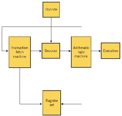
Register Set (RS): In this information is encoded, stored, and retrieved. The RS of this system contains
the following registers:
IR - holds the current instruction.
PC - holds the address of the next instruction.
Load - holds data loaded from memory.
Store - holds data being stored to memory.
SR - when an operation involves two operands, the status signals are updated. The SR can also
the used as an operand in arithmetic and logical operations.
All GPRs and the SR can be used in any operation except for the load and store instructions. Only
GPR can be used for loading and storing.
Instruction Fetch Machine: This machine fetches an instruction from external memory, and upon
completion of the instruction fetch cycle this machine signals the decoder to decode the instruction. This
machine utilizes a 3-bit up counter with an active low reset. the CPU changes states and begins to decode
the instruction.
Decoder: Upon completion of the instruction fetch cycle, the instruction is decoded. The decoder reads
bit 3 down to 0 of the IR, decides which of the sixteen operations the CPU needs to performs, and signals
one of the next states to
begin its operation.
Move Machine: The move machine controls all register movement. The most basic of these movements
is the movement of data from one GPR to another GPR. Upon completion of the movement of data, a new
instruction is fetched.
Arithmetic Logic Unit: The ALU performs arithmetic and logical operations on data. The data is taken
from two GPRs and is moved to the ALU. The result is stored in a GPR. For operations that involve one
operand, a GPR can be specified to store the result. The ALU supports two’s complement data.
Specified to store the result. The ALU supports two’s complement data.
III. PROPOSED TECHNIQUE
RISC
To reduce execution time by simplifying the instruction set of the computer. It has the ability to
execute one instruction per cycle by overlapping the fetch, decode, and execute phase of two or three
instructions using a procedure referred to as pipelining. Instructions are of a fixed number of bytes and
© 2014, IJCSMC All Rights Reserved 366 Combining with DSP:
A DSP is a specialized microprocessor with an architecture developed for the fast operational
needs of digital signal processing.
FPGA:
CLBs that provide the functional element to implement most of the logic gates. Input/output
blocks (IOBs) that provide the interface between the package pins and the internal logic delay-locked
loops (DLLs) that are used to distribute the clock and properly compensate the delays and blocked RAMs,
each of which has 4,096 bits
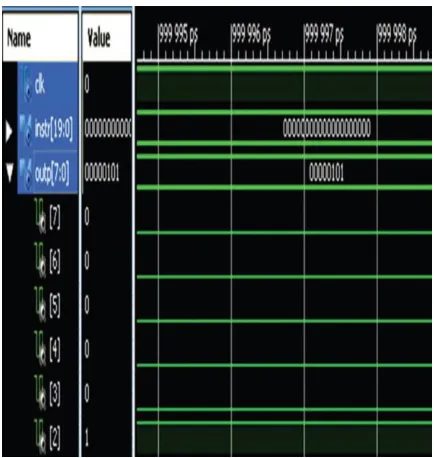
IV. SIMULATION RESULT
© 2014, IJCSMC All Rights Reserved 367
Figure 3 : Simulation of the OR gate of two 8-bit input Registers.
V. CONCLUSION
The design has been implemented and easily seen in the Model sim 14.0.0.200 windows as
waveforms. The simulation and results show that this design successfully offers a variety of features,
including arithmetic operations and logical operations. The design will be useful in several areas,
including Android phones. The implemented design easily can be seen in the waveform. Another great feature is that it’s easily upgraded by increasing the processor’s memory, and can be implemented with a
higher bit value. Using ModelSim operation can be implemented. The assembler of this processor is full
of macros that extend the native instruction set to facilitate low level programming.
REFERENCES
1) Kui Yi., WuHan, Yue-Hua Ding,”32 Bit Multiplication And Division ALU Design Based On RISC
Structure” International Joint Conference on Artificial Intelligence, pp. 761 – 764, 25-26 April 2009.
2) Ryszard Gal, Adam Golda, Maciej Frankiewicz, Andrzej Kos, “FPGA implementation of 8-bit RISC
Microcontroller for Embedded System”18th International Conference on MIXDES, pp. 323-328, 16-18
June 2011.
3) R. Kamal, “Microcontrollers: Architecture, Programming, Interfacing and System Design”
© 2014, IJCSMC All Rights Reserved 368
4)John L. Hennessy, and David A. Patterson, “Computer Architecture A Quantitative Approach”,4th Edition; 2006.
5)S. de Pablo, J.A. Cebrián, L.C. Herrero “A very simple 8-bit RISC processor for FPGA” FPGA
world Conference 2006, November 2006.
6)J.D. Luker and V.B. Prasad, “RISC System Design in an FPGA,” Proc. 44th IEEE 2001 Midwest
Symp. Circuits and Systems, 2001, pp.532–536.
7) L. Kaouane et al,” A Methodology to Implement Real-time Applications on Reconfigurable
Circuits”.
8)P. Kohlig et al, “FPGA Implementation of high performance “, In Proc. International Symposium
on Circuits and Systems, 1997.
9) Ryszard Gal, Adam Golda, Maciej Frankiewicz, Andrzej Kos,