Asynchronous Pulse Logic
Thesis by
Mika Nystrom
In Partial Fulfillment of the Requirements for the Degree of
Doctor of Philosophy
California Institute of Technology Pasadena, California
200l
©
2001Acknowledgments
What am I doing in graduate school? My interest in computing goes back to when I disassembled, with my father, an Original-Odhner pinwheel calculating machine. I must have been about four or five years old at the time, and like most four-or-five -year-olds who have a passing acquaintance with
addition and subtraction, arithmetic is something very mysterious. The sight of the many, many tiny gears in the insides of that calculator has dogged me ever since. I have been determined to figure out how it worked. Today I think I have a fair idea.
This thesis is first and foremost dedicated to my parents, who started it all-in more ways than one. I am sad to say that they did not live to see me through school; I should not have been here without their insistence on education before all else. I shall always be baffled by my mother's courage in sending me to a school where a foreign language--English-was the only one we young students could communicate in. Eventually it led to my leaving my native Sweden just as she once left her native Finland.
One's own insistence is not enough. I have been lucky to live in a world where willing and able teachers are plentiful. Starting with Lynn Carlisle, whom I still blame when my accent marks me a Midwesterner, I have had many: Maurice Naddermier, who first opened my eyes to the vastness of science; Simeon Leet, who in three years of high school taught me most of the mathematics that I know to this day and gave me a strong appreciation for the place of science and technology in the larger universe of human wisdom; and latest but not least, my advisor, Alain J. Martin, whose patience in the last seven years with the many things I have enjoyed myself working on has seemed infinite. I have had many other inspiring teachers in between; and if I were to list also those teachers that have taught me through their writings, the list would go on forever (some of their names appear in the Bibliography).
and much of what I write about here originally came from their minds and only made a detour through mine before landing on paper.
The members of my thesis committee, Andre DeRon, Alain Martin, Rajit Manohar, and Ali Rajimiri, have read the thesis carefully and suggested many changes. I have tried to control my own stubbornness and take as much of their advice as possible, but I have not always been successful in this.
Several others have read the thesis out of the goodness of their hearts and given me hundreds of helpful comments: Karl Papadantonakis, Cathy Wong, Eitan Grinspun, Paul Penzes, Abe Ankumah, and the anonymous Institute Proofreader. Especially Chapter 3 owes much of its Greek clarity to Karl's demands. Again, these kind readers' comments have had a powerful foe in my stubbornness, and remaining errors are all mine.
This thesis is written in English (or American; but I think they are the same), a language that I learned (from Lynn) when I was four years old. Writing a Ph.D. thesis is something one tries to do carefully, so before I embarked on it, I decided to try to improve my writing by reading up on the English language. I may have succeeded, but I have also acquired some unusual habits of expression that I should perhaps caution the reader of. (Such as obstinately putting prepositions at the ends of sentences whenever I deem it appropriate.) These habits have been inspired by H. W. Fowler.1 As I am writing computer-science English, I am permitted a great degree of leeway. I do not know why so many computer scientists write such sloppy English; we that are used to expressing ourselves with such exactitude when dealing with machines seem to of tell fall flat on our faces when trying to deal with human readers. I have tried to use my technical writer's leeway to write unambiguously rather than sloppily; in this I have made fewer concessions to convention than Fowler himself would have. No doubt sometimes all that I have achieved is annoyingly unconventional writing, and for all my efforts I have not managed to completely banish the sloppy mistakes; I am for instance convinced that hyphenation in English, especially noun-stacking technical English, walks a thin line between illogicality and illegibility. I cannot blame Fowler for these failings: they are due to my own pedantry and my sometimes foolish wish for consistency.
We live in a practical world, and research clops not come of the mind alone. Many generous sponsors have made the work described here possible: it has been supported by the Defense Advanced Research Projects Agency (DARPA) for a long time, and I have been directly supported by the Okawa Foundation and by a two-year Graduate Research Fellowship from IBM Corporation. The computers used for the work were donated by Intel Corporation.
Caltech is a truly remarkable place filled with remarkable persons. On the practical side, my stay as a graduate student has been made less stressful by the hard work of many Computer Science staff members; especially Cindy Ferrini, Jeri Chittum, and Betta Dawson.
Abstract
This thesis explores a new way of computing with CMOS digital circuits, single-track-handshake
asynchronous pulse-logic (STAPL). These circuits are similar to quasi delay-insensitive (QDI) cir-cuits, but the normal four-phase QDI handshake is replaced with a simpler two-phase pulsed hand-shake. While a delay-insensitive two-phase handshake requires complicated decoding circuits, the pulsed handshake maintains the simpler, electrically beneficial signaling senses of four-phase hand-shaking by using timing assumptions that are easy to meet.
We cover many aspects of designing moderately large digital systems out of STAPL circuits, from the communicating-process level to the production-rule and transistor level.
We study the theory of operation of pulsed asynchronous circuits, starting with simple pulse repeaters; hence we progress to a general theory of operation for pulsed asynchronous circuits. This theory is a generalization of the theory of operation of synchronous digital circuits.
We then develop the family of STAPL circuits. This is a complete family of dataflow processes: the presented circuits can compute unconditionally as well as conditionally; they can also store state and arbitrate.
Next, we present some aspects of automatic design-tools for compiling from a higher-level de-scription to STAPL circuits. Many of these aspects apply equally well to tools for QDI circuits; in particular, we study boolean-simplification operations that may be used for improving the perfor-mance of slack-elastic asynchronous systems.
Finally, a simple 32-bit microprocessor is presented as a demonstration that the circuits and design methods work as described. Comparisons arc made, mainly with QDI asynchronous design-styles: SPICE simulations in 0.6-ILm CMOS suggest that a system built out of automatically com-piled STAPL circuits performs at about three times higher throughput (650-700 MHz in 0.6-lLm
CMOS) compared with a similar system built out of carefully hand-compiled QDI circuits; the STAPL system uses about twice the energy per operation and twice the area; in other words, the STAPL system improves on the QDI system by four to five times as measured by the Et2 and At2
Contents
Acknowledgments
Abstract
1 Introduction
1.1 The VLSI design process . 1.2
1.3 1.4
1.5
From physics to computer science . Asynchronous digital design Asynchronous design-styles 1.4.1 Bundled-data design
1.4.2 Delay-insensitive design-styles. Contributions
2 Preliminaries
2.1 Quasi delay-insensitive design 2.2 High-speed CMOS-circuits . .
2.3 Asynchronous protocols and delay-insensitive codes 2.4 Production rules . . . . .
2.5 The MiniMIPS processor . 2.6 Commonly used abbreviations.
3 Asynchronous-Pulse-Logic Basics 3.1 Road map of this chapter
3.2 The pulse repeater . . . .
3.2.1 Timing constraints in the pulse repeater 3.2.2 Simulating the pulse repeater .
3.2.3 The synchronous digital model 3.2.4 Asymmetric pulse-repeaters 3.3 Formal model of pulse repeater . .
3.3.1 3.3.2 3.3.3 3.3.4
Basic definitions . , . . . . Handling the practical simulations Expanding the model
U sing the extended model 3.3.5 Noise margins . . . .
3.4 Differential-equations treatment of pulse repeater 3.4.1 Input behavior of pulse repeater
3.4.2 Generalizations and restrictions .
4 Computing With Pulses 4.1 A simple logic example. 4.2 Pulse-handshake duty-cycle
4.3 Single-track~handshake interfaces
4.4 Timing constraints and timing "assnmptions" 4.5 Minimum cycle~transition-counts . . . 4.6 Solutions to transition-count problem 4.7 The APL design-style in short . . .
5 A Single-Track Asynchronous~Pulse-Logic Family: 1. Basic Circuits 5.1 Introduction.
5.2 Preliminaries 5.2.1
5.2.2 5.2.3 5.2.4 5.2.5
Transition counting in pipclined asynchronous circuits Transition-count choices in pulsed circuits
Execution model . . . . Capabilities of the STAPL family. Design philosophy
5.3 The basic template . 5.3.1 Bit generator 5.3.2 Bit bucket. . 5.3.3 Left-right buffer
5.4 Summary of properties of the simple circuits.
25 27 28 30 31 31 33 37 39 40 44 46 47 48 49 49 51 51 51 52 53 56 56 57 58 58 62 66 71 6 A Single-Track Asynchronous~Pulse-Logic Family: II. Advanced Circuits 73
6.1 Multiple input and output channels. 73
6.1.1 Naive implementation . . . . 75
6.1.4 Timing assumptions 6.2 Generallogic computations
6.2.1 Inputs whose values are not used 6.3 Conditional communications . . . .
6.4
6.5
6.6
6.7 6.8
6.3.1 The same program can be expressed in several ways 6.3.2 Simple techniques for sends . . . . 6.3.3 General techniques for conditional communication-actions Storing state . . . . . .
6.4.1 The general state-storing problem 6.4.2 Implementing state variables 6.4.3 Compiling the state bit Special circuits . .
6.5.1 Arbitration
6.5.2 Four-phase converters Resetting STAPL circuits . .
6.6.1 Previously used resetting schemes 6.6.2 An example . . . . . . . . 6.6.3 Generating initial tokens.
How our circuits relate to the design philosophy . Noise . . . .
6.8.1 6.8.2 6.8.3 6.8.4 External noise-sources Charge sharing Crosstalk . . . Design inaccuracies .
7 Automatic Generation of Asynchronous-Pulse-Logic Circuits 7.1 Straightforwardly compiling from a higher-level specification. 7.2 An alternative compilation method
7.3 What we compile. 7.4 The PL1 language
7.4.1 Channels or shared variables?
7.4.2 Simple description of the PL1 language 7.4.3 An example: the replicator
7.5 Compiling PL1 . . . 7.6 PL1-compiler front-end
7.6.1 Determinism conditions
7.6.2 Data encoding . 7.7 PL1-compiIer back-end. 7.7.1 Slack . . . . 7.7.2 Logic simplification. 7.7.3 Code generation ..
8 A Design Example: The SP AM Microprocessor
8.1 The SP AM architecture 8.2 SPAM implementation
8.2.1 Decomposition
8.2.2 Arbitrated branch-delay 8.2.3 Byte skewing
8.3 Design examples .. 8.3.1 The PCUNIT . 8.3.2 The REGFILE
8.4 Performance measurements on the SPAM implementation 8.4.1 Straightline program . . . .
8.4.2 8.4.3 8.4.4 8.4.5
Computing Fibonacci numbers Energy measurements . . . . .
Summary of SPAM implementation's performance Comparison with QDI . . . .
9 Related Work
9.1 Theory . . . . 9.2 STAPL circuit family. 9.3 PL1 language . . . . . 9.4 SPAM microprocessor
10 Lessons Learned
10.1 Future Work 10.2 Conclusion
A PLI Report
A.1 Introduction. A.I.1 Scope
A.I.2 Structure of PL1 A.2 Syntax elements
A.2.1 Keywords
A.2.2 Comments. A.2.3 Numericals A.2.4 Identifiers
A.2.5 Reserved special operators. A.2.6 Expression operators A.2.7 Expression syntax A.2.8 Actions
A.3 PLI process description A.3.1 Declarations .
A.3.2 Communication statement . A.3.3 Process communication-block A.4 Semantics
A.4.1 Expression semantics . A.4.2 Action semantics A.4.3 Execution semantics A.4.4 Invariants
A.4.5 Semantics in terms of CRP A.4.6 Slack elasticity
A.5 Examples
B SPAM Processor Architecture Definition B.1 Introduction.
B.2 SP AM overview .
B.3 SPAM instruction format
B.4 SPAM instruction semantics . B.4.1 Operand generation B.4.2 Operation definitions . B.5 Assembly-language conventions
B.5.1 The SPAM assembly format .
C Proof that Definition 3.2 Defines a Partial Order C.1 Remark on Continuity
List of Figures
2.1 One stage of domino logic . . . . 2.2 Dual-rail encoding of one bit of data.
3.1 Three-stage pulse repeater. 3.2 Five-stage pulse repeater. .
3.3 A long pulse almost triggers a pulse repeater twice. 3.4 Shmoo plot for three-stage pulse repeater.
3.5 Shmoo plot for five-stage pulse repeater. .
3.6 Input-output relationship of pulse lengths for five-stage pulse repeater; this particular circuit stops working for input pulses longer than 1.47 ns.
3.7 Qualitative interpretation of shmoo plots. . ..
8 9
16 17 19 19 20
20 22
3.8 Mapping of input to output pulse parametf~rs. . 23
3.9 Asymmetric 3-5-stage pulse repeater. . . . 25
3.10 (a) the function
f
and two members j, k E P(P). Here j :::;f :::;
k. (b) parameter-space representation of sets J(f) and K(f) and the points j and k (more properlyp-l(j) and P-l(k)) picked by M. 29
3.11 Input circuitry of a pulse repeater. 33
3.12 Pulse repeater modeled with inverting ill(~rtial delay. 35 3.13 Two different input-pulse scenarios and tht~ir corresponding intermediate-node values
and output values. . . . . 36
4.1 Input transistors in QDI merge. 41
4.2 APL circuit, version with diodes. 41
4.3 APL circuit, version with diodes and reset transistors. 42
4.4 APL circuit; diodes implemented with transistors. 43
4.5 Pseudo-static C-element. . . . . 47
5.2 Path from input's arriving to its being removed in STAPL circuit: dotted, forward path; dash-dotted, backward path. . . 55
5.3 Forward (compute) path of STAPL bit generator. . 60
5.4 Complete STAPL bit generator. . 61
5.5 STAPL bit bucket. . . . 65
5.6 STAPL left-right buffer. 68
5.7 Paths implementing the delays Strue, Bfalse, :Ctrue, and Xfalse. 70
6.1 Schematic version of unconditional STAPL template. 83
6.2 Schematic version of conditional STAPL template. 88
6.3 Basic state bit. . . 93
6.4 Naive state-variable compilation. 94
6.5 Sophisticated state-variable compilation. 97
6.6 "Mead & Conway" CMOS arbiter. 98
6.7 Complete STAPL ARB process. . . 98
6.8 QDI-to-STAPL interfacing cell built from a QDI and a STAPL buffer. 100 6.9 STAPL-to-QDI interfacing cell built from a STAPL and a QDI buffer. 101 6.10 Circuit alleviating charge-sharing problems. Resistor implemented with weak transistor. 108 6.11 "Load lines" of pulsed circuit. 1: pulse becomes lower when the circuit is overloaded;
2: pulse becomes lower and longer. . . . . 110
7.1 Structure of the PL1 compiler. Files are shown in dashed boxes; program modules in solid. . . 119 7.2 Relevant parts of declaration of sum-of-products data structure in Sop. i3. . 129 7.3 Modula-3 code for boolean simplification. . . 130
8.1 Sequential CRP for SPAM processor. . 134
8.2 Overview of SPAM decomposition. . . 134
8.3 Three ways of distributing control, shown OIl a hypothetical datapath operating on 32
bits encoded as 16 1-of-4 values. (a) MiniMIPS method: two-stage copy to four byte-wide processes. (b) Asynchronous-filter method: linear tree (list) of control copies to 16 processes operating on 1-of-4 data (bit skewing). (c) SPAM method: linear tree of control copies to four four-way copies and thence to 16 processes operating on 1-of-4 data. . . 138 8.4 Top-level CAST decomposition of SPAM PCUNIT (without arbiter). . 141 8.5 Process graph of PCUNIT. Data channels are drawn solid; control channels dotted.
8.6 PL1 program for a single 1-of-4 process of psel.
8.7 PL1 program for pcunitctrl.
143 144 8.8 Block diagram of pc incrementer; layout alignment. Flow of data is from left to right. 145
8.9 Block diagram of pc incrementer; time alignment. . 146
8.10 Behavior of expc [1J after reset; no branches. . . . 148 8.11 Behavior of control for pc-selector psel; a branch is reported at t =12 ns. 148 8.12 Current draw of PCUNIT in amperes; no branching. Go active at t = 6.5 ns. . 149 8.13 Current draw of PCUNIT in amperes; constant branching after t = 12 ns. Go active
at
t
= 6.5 ns. . . 150 8.14 Arrival of least and most significant 1-of-4 codes of pc. 150 8.15 Charge sharing in the pc incrementer. . . 151 8.16 Circuit diagram of compute logic for the upper 1-of-4 code in pc-incrementer. 152 8.17 Top-level CAST decomposition of SPAM REGFILE. . . . 154 8.18 Process graph of REGFILE. Data channels are drawn solid; control channels dotted. 155 8.19 Block diagram of 8 x 8 register-core cell; input and output channels are each four1-of-4 codes. . . . 156 8.20 Circuitry associated with each pair of state bits in register core. Dummy-write
cir-cuitry not shown. . . . . 157 8.21 Overall arrangement of register-core cell. A two 1-of-4-code tall, three-register wide
chunk is shown. . . 158
8.22 SPAM program for computing Fibonacci numbers. 159
8.23 Part of the critical-path transition-trace of running the program of Figure 8.22. Time goes upwards; each transition delay is counted as 100 time units.
8.24 SPAM program for computing Fibonacci numbers, unrolled once.
Chapter
1
Introduction
For 'tis your thoughts that now must deck ollr kings, Carry them here and there; jumping o'er times, Turning th'accomplishment of many years
Into an hour-glass: for the which supply,
Admit me Chorus to this history;
Who, prologue-like, your humble patience pray,
Gently to hear, kindly to judge, our play.
- William Shakespeare, The History of King Henry the Fifth (1599)
In January of 1979, the first of a series of conferellces on "Very Large Scale Integration" took place at Caltech. The two keynote speakers, Gordon :!VIoore of Intel and Carver Mead of our Computer Science Department, both spoke of the same concern, but from two very different viewpoints. Their concern was design complexity.
Moore, the conservative industrialist, questioned whether the electronics industry was really ready for VLSI: "If the semiconductor industry had a million-transistor technology like VLSI," he wrote in the article accompanying his talk, "I'm not so sure it would know what to do with it." [62] He seemed to find it a far-fetched idea that a circuit designer should possibly know how to make use of a canvas large enough to hold a system as complex as VLSI would allow.
the large-system design problem would in time be tackled, as the fundamental problems of device physics and fabrication had been before it.
A quarter century will soon have passed since these words were written. In this time, there have been great advances, along the lines Mead predicted, in circuit design techniques and in computer-aided design and design automation. But the fact remains that most of today's VLSI systems are understood in terms of the same finite-state machines that were used for describing the mainframes of the 1960's; the fact remains that highly concurrent systems are poorly understood, especially by circuit designers.
The inevitable conclusion is that today';; multi-million-transistor chips have been made possible not mainly by new fundamental ideas, but by the almost superhuman efforts made in exploiting the old ones. Though the fact may puzzle him that reads in today's newspapers that he stands in the middle of a "tech revolution," Carver Mead's VLSI revolution, 25 years in coming, is yet unfulfilled.
1.1
The
VLSI
design process
VLSI-system design is the process of implementing and realizing a system specification, the archi-tecture, as an electronic circuit. We shall assume that the architecture is given to us and that the fabrication is not our concern. Longtime tradition, due to IBM [11], divides the design process into two stages beyond computer architecture: irnple'fnentation of the architecture by a micro-architecture and realization of the micro-architecture by a physical circuit design.
The border between implementation and realiza.tion, like that between the United States and Mexico, is an artificial demarcation drawn for political purposes. The VLSI border traditionally serves to separate high-level logical reasoning from electronic-circuit design, tasks usually performed by different people, or at least by different software systems.
1.2
From physics to computer SCIence
1.3
Asynchronous digital design
Poor performance is usually unacceptable for a VLSI system. Optimists have long studied asyn-chronous design techniques, hoping that they have found at least a partial solution to the design problem. While it is true that proponents of asynchronous design like claiming that asynchronous circuits offer speed and power advantages, the author believes that the main advantage of asyn-chronous design is more subtle than these: it is the designer's ability of easily composing circuits that operate at different points in the design space (characterized by speed, power, and design effort) without destroying the beneficial properties of any of the circuits.
What makes a digital system asynchronous'! A system is asynchronous if, in short, it does not use a clock for sequencing its actions. Asynchronous logic has been used for computer design since the 1950's, when several members of the ILLIAC series of computers were designed partly asyn-chronously [45]; somewhat later, Digital Equipment Corporation's PDP-6 computer was a modest commercial success [20].
What unites all methods of asynchronous circuit design is that they all strive for making the speed of computing dependent on the operations that are being carried out. A slow operation is allowed to take longer than a fast one; the system continues to the next operation only once the previous one is completed.
It is as if we could assemble a troika consisting of an Arabian, a Shetland pony, and a draught horse, without losing the useful qualities of the individual horses. If we should try this with real horses, the harness would act much as the clock does in a synchronous system and render the exercise pointless. But the asynchronous troika may he ahle to pull its load better than even a well-matched synchronous team, because the horses are not harnessed together by the clock-the draught horse does not have to keep up with the Arabian, and we do not have to feed the big horses if we only have need for the pony.
By allowing us to divide up a system into smaller, more independent pieces, the asynchronous design technique simplifies the large-system design problem: the main goal of asynchronous design is addressing Carver Mead's concern of 1979.
1.4
Asynchronous design-styles
In contrast, the chief difficulty in asynchronous design is knowing when a specific computation is done. If we encode data in the same way as in a synchronous system, e.g., using two's-complement numbers, and start an operation f(x), and the number "5" should appear on the result bus of our asynchronous system, how are we to know that it signifies the result of the present computation, and not of the previous? Worse, might it not be the bitwise combination of the results of the previous and current computations?
1.4.1
Bundled-data design
The early asynchronous computers were designed ill what we shall call the bundled-data style. De-signing in this style, the designer assumes that he can build a delay that matches whatever the delay is of the computation that he is really interested in. This matched delay is used as an "alarm clock" that is started when
f
(x) is started and that rings when we can be sure thatf
(x) has been completely computed. The design style is called bundled data because the data travels in a "bundle" whose timing is governed by the control signal that we called the "alarm clock." As one might guess, arranging for the matched delay is the Achilles' heel of the bundled-data style. If the delay is too short, the system will not work; if too long, then it will work slowly. Especially if computation times are data-dependent, the matched delay can easily become a designer's nightmare. The matched delay mechanism's working rests on a form of a pn;ori knowledge of relative timing; we shall call making use of such knowledge a timing (lss'umption.1.4.2
Delay-insensitive design-styles
Originally conceived of at about the same time as the bundled-data design-style, delay-insensitive logic design attempts using the data bits themselves for sequencing. By making every input transition (change in logic level) cause, either in itsdf or within a cohort of input transitions, an output transition or a detectable pattern of output transitions, we can at least make interfaces between processes delay-insensitive.
Systems built using the delay-insensitive philosophy range from the speed-independent investi-gated by D. E. Muller in the 1950's [63], which work under the assumption that all wire delays are negligible compared with the operator delays (which may be of any length), to the truly delay-insensitive, in which both operator delays and wire delays may be arbitrary. Martin has shown that, using a reasonable operator model,J truly delay-insensitive systems are of little use [51]; the work in our research group has mainly beel! within the q'u,(lsi delay-insensitive (QDI) model, which is essentially Muller's speed-independent model with information added for distinguishing between
wires whose delays must be short compared with the operator delays and wires whose delays may be arbitrarily long.
We cannot possibly do justice to the many different design methods that have been proposed for asynchronous-circuit design;2 bundled-rlata and QDr rlesign will however serve as convenient extremes that we can compare with.
Assembling a working system out of QDI parts is almost frighteningly easy: start from a correct sequential program, decompose it into communicating processes, compile these processes into cir-cuits, put the pieces together, and everything works. The chief advantage of this way of designing systems is that once we have decomposed, the design style is completely modular: there is no implicit use of global information (i.e., no clock), and the different parts can be designed independently.
In this sense, QDI design comes close to finally putting Carver Mead's concern to rest. But there is one difficulty with QDr design: the requirement that the circuits work properly even if
all operator delays were to vary unbouncledly is a difficult one to satisfy; our satisfying it involves inserting much circuitry whose only purpose is checking for the occurrences of transitions that we may know would in any case take place.:' We should say that QDI systems must still be designed "within reason": it is possible to make things not work by designing them very poorly; likewise, it still takes considerable work and skill to achieve good performance. Yet, with these things in mind, the message-passing QDr design-style allows the design of large, well-performing systems with relatively little design effort [53, 18, 55].
1.5
Contributions
This thesis makes its main contribution by developing a design style that allows making use of limited amounts of timing information, i.e., limited use of timing assumptions, without destroying the most important, system-simplifying property of QDI design, namely that of the data's carrying its own timing information. We do this by replacing some of the four-phase (return-to-zero) handshakes in a QDr circuit with pulses, thus breaking the timing dependencies that are the source of the performance problems of QDI circuits. Our ultimate goal is that of improving the performance of modular asynchronous systems so much that it becomes possible to use asynchronous techniques for implementing large systems that perform well, yet are easy to design.
The organization of the thesis is as follows:
2The interested reader should see Hauck's paper for a b;tlanced introduction [34J.
I. \Ve develop a theory that accounts for the proper functioning of pulsed asynchronous circuits (Chapter 3).
II. We develop a new target for the compilation of CHP programs, the single-track-handshake asynchronous-pulse-Iogic (STAPL) circuit (Chapters 5 and 6). These circuits are as easy to compose as QDI circuits, yet they operate faster: they have fewer transitions per execution cycle (10 instead of QDI's 18 for many nontrivial circuits), and they have less loading from p-transistors (no input-completion circuitry ill most cases, and even when it is present, it has no p-transistors).
III. We explore some properties of Pipeline Language 1 (PLl), a simple yet expressive language for describing asynchronous bit-level processes (Chapter 7). PLI is a convenient language for expressing the behavior of basic dataflow-style processes. It succinctly captures all the capabil-ities we should like to have and that are easy to implement for simple asynchronous processes. The particular capabilities that we choose for the language are inspired by the MiniMIPS work: we thus have evidence that the capabilities are enough for implementing large and well performing asynchronous digital VLSI systems. It is much easier to work with descriptions at this level than in terms of production-rule systems; compared with CHP programs, the PLI language allows only a subset that can be :.;traightforwardly and automatically compiled. The PLI language is intended to be used for both STAPL and QDI design.
IV. Putting the methods developed in previous chapters to the test, we study a microprocessor design consisting of STAPL circuits, most of which were themselves designed using the PLI language (Chapter 8). The microprocessor is a simple 32-bit one; the design shows how best to take advantage of the capabilities of the STAPL circuit family. The results of the test are good: the STAPL family is shown to he capable of significantly higher throughput than QDI circuits at a small extra cost in energy; the overall improvement using the Et2 metric is
Chapter
2
Preliminaries
-And why not the swift foot of Time? lwei not that been as proper?
-By no means, sir. Time travels in divers paces 1vitil divers persons.
~- William Shakespeare, As You Like It (1599)
2.1
Quasi delay-insensitive design
This thesis aims at establishing a new t.arget for hardware designers; while asynchronous, the new pulsed-logic design-style depends on timing assnmptions for working properly, which quasi delay-insensitive (QDr) circuits do not. Still, many of the design issues are very similar, especially at the higher levels of the design; consequently, we shall be able to reuse much of what is known of QDr design.
We shall use much of the same terminology and not.ation as QDr designers do. To wit, we shall compile our circuits starting from the Communicat.ing Hardware Processes (CHP) language, a language based on Hoare's Communicating Sequential Processes (CSP) [36J; we shall describe our communication protocols using the not.ation of the Handshaking Expansion (HSE) language used by QDr designers; we shall describe our t.ransistor networks using the Production-Rule Set (PRS) notation. These languages are all explained in detail by Martin [48, 54]; some more recent extensions to CHP, whose syntax was suggested by Matthew Hanna, are described by Hanna (33J and the author [66].
2.2
High-speed CMOS-circuits
Vdd
c-4
out
in
L-_-¥--"",---'
network of
n-transistors
c--1
GND
Figure 2.1: One stage of domino logic.
Here we shall only cover a few issues in nomenclature. A basic CMOS domino-logic "stage" is shown in Figure 2.1. The part on the left. of the f:igun~ is the "precharged domino" part of the circuit. When the control signal C goes low, the stage precharges--the node x rises and the output out falls. When C next goes high, depending on the values on the in wires, the domino mayor may not "fall" (i.e., x mayor may not fall to GND). The llame "domino logic" comes from these circuits' ability of being cascaded within a single clock-phase in a synchronous system. Confusingly, while Figure 2.1 depicts a single "domino stage," the same structurp can also be called two "stages of logic" -the domino block plus the inverter. In the design style that we use, a block like this also implements an entire "pipeline stage"; i.e., cascaded dominos cycle independently (to an extent determined by the
"reshuffling" of the handshake).
The important features of domino logic: are as follows. There are few p-transistors; because of the much higher mobility in silicon of electrons compared with holes, this means that domino logic will usually be much faster than combinational logic, where pulling up the outputs has to be handled by the inputs. Furthermore, if we wish to cascade the dominos, each computation stage takes two logic transitions (one for the domino, one for the inverter)-this we call the forwarrllatency of the stage; alternating "n-dominos" with "p-clominos" is possible, hut the performance gain, if any, compared with standard domino logic, is small; owing to the lIlany p-transistors in the p-dominos, this style can indeed be slower. An important drawback of domino logic is that it is more sensitive to different kinds of noise than combinational logic is.
Rail Value
x.O false true false true
x.l false false true true
Meaning No data :r:
=
0 :r;=
1 IllegalFigure 2.2: Dual-rail encoding of one bit of data.
can be required by asynchronous data-transfer protocols.
2.3
Asynchronous protocols and delay-insensitive codes
Asynchronous systems are based on handshaking protocols; i.e., two processes wishing to transfer data between each other synchronize the data transfers with signals that the processes themselves generate. It is most straightforward for us first to envision the handshake itself and then to add the data transfers in later. This way of designing things allows transferring data using conceptually simple protocols. One property that must be satisfied by the data is that it is encoded using a
delay-insensitive code.
This means informally that the data encoding contains the same information that was present in the original "bare" handshake (i.e., data present or not-present) and that the data is encoded so that transitioning between the data present and not-present states is free from timing assumptions (i.e., it does not matter in which order the transitions are received). The most basic encoding that satisfies these conditions is the dual-rail ellcoding of a single bit (Figure 2.2); one that will also be seen often in this thesis is the l-of-4 encoding of two bits.
Generalizing from bare handshakes to using delay-insensitive codes leads naturally to needing circuits for determining whether data is present or not-present. This we loosely refer to as "comple-tion circuitry." For instance, a two-input OR-gate can be used for completing a dual-rail channel, as can a four-input OR-gate for a l-of-4-cocled channel.
2.4
Production rules
In this thesis, we shall not generally describe circuits at the level of transistor netlists; this would be unnecessarily much detail. Instead, we shall use pr-odnction rules. A production rule (PR) is a statement of the form
G --7 x := c
x := true as
xt
(read as "x up") and .'f := false as 1;+ (read as "x down"). At the circuit level, the effect of such an elementary assignment is a transition on 1: from a low to a high or from a high to a low voltage.In a given system, we must necessarily have rules for the setting of each node x that transitions more than once both to true and to false; the combination of the two rules is called an operator.
In other words, an operator is a device with one or more inputs and a single output. The mapping from operators to circuit gates is fairly direct, but we do not consider it in detail in this thesis; nor do we consider layout issues in detail.
Before proceeding, it must be pointed out that although we use the same notation, our using timing assumptions means that we cannot ascribe quite the same semantics to HSE and PRS as we can in QDI designs. We shall have more to say about this later; in short, we disallow "stuttering" in HSE and we shall use a timed execution model for production rules instead of the weakly-fair-interleaving model that can be used for QDI circuits.
2.5
The MiniMIPS processor
The MiniMIPS processor, designed by the Caltech group during 1995-1998, represents the state of the art in QDI asynchronous design today [55].
The MiniMIPS processor consists of two million transistors; it has been fabricated in 0.6-JLm
CMOS, and in this technology, it runs approximately 170 MHz at the nominal process voltage (3.3 V).
A few notable features of the MiniMIPS processor an~ the following:
• Almost complete reliance on QDI circuits. (The exceptions are the low-level implementation of the cache-write mechanism and the off-chip bundled-data asynchronous interface.)
• Extensive use of 1-of-4 data-encoding to minimize completion delays and save switching power.
• Universal use of precharged, pseudo-static1 domino-logic.
• A deeply pipelined design with buffering in every domino stage. The processor can execute many programs at an average speed of 182
/1
logic transitions per fetch cycle.As important as the MiniMIPS processor itself a.re the techniques used to design it:
• Initial specification as a sequential CHP program and stepwise refinement to a collection of concurrent processes.
• Use of slack elasticity [45] to allow variable latencies yet ensure deterministic behavior.
• Final, formal specification in terms of a hierarchical production-rule set (PRS), using the CAST language.
• Universal use of full-custom physical design, in terms of a magic cell hierarchy. Several man-years were spent on this aspect of the design.
2.6
APL BDD C CAST CHP CMOS CSP DI DRAM ERGND
HP HSE IBM MIPS MOS PCHB PLI PR PRS QDI RIse SPAM SRAM STAPL Vdd VLSI WCHB 12Commonly used abbreviations
Asynchronous pulse-logic Binary-decision diagram Consensus (in "C-element")
Caltech asynchronous synthesis tools (hardware description language) Communicating hardware processes
Complementary metal-oxide-semiconductor [field-effect transistor] Communicating sequential processes
Delay insensitive
Dynamic random-access memory Event rule
Ground (circuit node) Hewlett-Packard [Corp.] Handshaking expansion
International Business Machines [Corp.]
Microprocessor without interlocked pipeline-stages Metal-oxide-semiconductor [field-effect transistor] Precharged half-buffer
Pipeline language 1 Production rule Production-rule set Quasi delay-insensitive
Reduced-instruction-set computer
Simple pulsed asynchronous microprocessor Static random-access memory
Single-track-handshake asynchronous pulse-logic Positive power supply (circuit node)
13
Chapter 3
Asynchronous-Pulse-Logic Basics
All delays are dangerous in war.
- .101111 Dryden, Tyrannic Love (1669).
Over the years, asynchronous design techniques have gone from Muller's simple handshaking circuits and the carefully timed bundled-data circuits used in the PDP-6 to the sophisticated, yet easy to design, dataflow techniques used for the MiniMIPS design. It remains, however, that the MiniMIPS processor operates, under ideal conditions, at a fetching rate of 182
/3
CMOS transitions per instruction fetch, and designing a QDI microprocessor that fetches much faster than this seems an impossible challenge. This number compares favorably with the performance achievable by most synchronous design techniques, but it falls short of the 10--14 transitions per cycle that the most aggressive (and hard-working) synchronous designers achieve.The barrier that prevents QDI circuits from achieving higher performance lies in the QDI hand-shake. By insisting on the four-phase handshake, e.g.,
* [
[li]; (compute outputs); lot; [.h]; loJ- ],we demand that any process in our system shall, after it has acknowledged receipt of its inputs, wait for those inputs to reset to neutral. This is expensive because checking inputs' neutrality is done in p-transistors: hence it must be decomposed into several stages, and it also loads the inputs heavily. (Of course, switching to inverted logic docs no good since then computing the outputs and checking the validity of the inputs must instead be done in p-transistors, which would be even worse than before.) The most trivial four-phase-handshaking QDI circuit takes ten transitions per cycle,! and anything nontrivial takes 14; inescapably, the complicated control-processes take 18. (These numbers are taken from the MiniMIPS [55] and Lines's work [43].)
Various authors have suggested that the solution to the performance problems that plague four-phase QDr circuits is that we should use two-four-phase signaling instead. Many variants exist; the
14
simplest is:
* [
[Ii -=I- 10]; (compute outputs); 10:= li ]Some things can be implemented well with this protocol, but designers struggle fruitlessly with anything but the simplest specifications when they must design logic. This is why: on each iteration of the loop, the sense of the input signal changes. At one moment, an input near Vdd means a true input; at another, it means a false input. Who can make sense of that?::!
What we want is a design style that combines the straightforward logic of four-phase QDI with the timing of two-phase logic. Obviously, we cannot expect to have all the desirable properties at once. Accordingly, we shall no longer demand that the circuits be QDI; yet they will in many ways operate similarly to the QDI circuits we used in the MiniMIPS.
But is it even possible to use the MiniMIPS design-style for designing anything but QDI circuits; shall we not have to abandon all that we know of asynchronous design and start over?
It turns out that most QDI circuits that have heen designed can be sped up considerably by introducing weak timing-assumptions, without our having to rethink the high-level design. The reason for this is simple: while using a four-phase handshake for implementing two synchronization actions is certainly possible (indeed, this technique is used in some special circuits, such as the distributed mutual-exclusion circuit designed by Martin [50]), this is not commonly done. In the dataflow-style processes used in the MiniMIPS, it is never done. Hence, out of the four phases of the four-phase handshake, only two are used: send and acknowledge. The remaining two, resetting the data and resetting the acknowledge, are not used for synchronization. These phases are entirely superfluous from the point of view of the specification.
Each phase consists of two actions: an assignment and the wait for that assignment. We can make use of the phases' being superfluous by eliminating the waits, even though we keep the assignments; by removing the waits, we get the synchronization behavior of two-phase handshaking; but by keeping the assignments, we keep the encoding properties of four-phase. What we propose doing is allowing communicating circuits to reset their interface nodes in parallel; in other words, once we acknowledge an input, we assume it will reset "quickly." This achieves the desiderata: the inputs may still always be in positive logic, yet their synchronization behavior will have many of the characteristics of two-phase signaling, since we only wait for the first phase of the inputs. Waiting for the first phase of the inputs is anyway normally required for computing the outputs, so what remains will definitely be closer to optimal.
In this chapter, we shall study a few simple pulsed circuits and then develop a theory that may be used to account for the proper functioning of a wide class of pulsed circuits and show how that
15
theory may be applied to the specific simple pulsed circuits.
3.1
Road map of this chapter
This is the most challenging chapter of this thesis as we make the needed connection between physics and computer science. So that the reader will not get lost in the chapter, let us first discuss the main points.
We shall first study the designing and simulating of a basic pulsed asynchronous circuit, viz. the pulse repeater. This will be an ad hoc discussion based on properties easily observable by and well-known to the electrical engineer: pulse lengths:l (widths) and heights.
Secondly, we shall explore why these simple and readily observable properties are not enough for describing the full range of possible pulse-repeater behaviors. Simply speaking, the essential shortcoming of the pulse length and pulse height is that these two properties, while they may suffice for specifying a testing pulse that is applied to a circuit, do not suffice for completely describing the shape of the output waveform produced by that circuit.
Thirdly, we shall generalize the legal-logic-range-noise-margin argument commonly made for es-tablishing the correctness of traditional synchronous circuits. This generalizing serves two purposes: on the one hand, it establishes a framework that we can understand the logic family of Chapters 5 and 3 within; on the other hand, it serves the wider purpose of taking a baby step towards establish-ing a formal model for the functionestablish-ing of asynchronous circuits with the simple understandability of the synchronous model. The mathematical argument in this section may seem overly formal, but it is really a straightforward generalization of the synchronous argument.
In generalizing we consider uncountably infinite sets of waveforms instead of the simple voltage-ranges used by the synchronous argument. By spncifying the sets of waveforms as "the set of all functions f(t) such that each f(t) is bounded below by the function j(t) and above by k(t)," we reduce the argument to one where j(t) and k(t) play the leading rOles instead of the much more cumbrous infinite sets of functions. This corresponds to understanding the synchronous argument in terms of the boundaries between the voltage ranges rather than having to consider every possible intermediate voltage separately.
Fourthly, we shall recognize that, given certain desirable properties of the circuits that we study, establishing the correctness of an asynchronous-pulse-logic family can be clone entirely in terms of functions j(t) and k(t); we shall determine what properties are necessary for allowing this vast simplification.
Lastly, we shall argue that the pulse n~peaters we first studied in such an ad hoc way actually satisfy the conditions allowing the simplification. At this point, we shall have to appeal to more
16
vaguely known things, such as transistor equations and circuit parameters; this argument is hence specific to the kind of circuits we are studying.
3.2
The pulse repeater
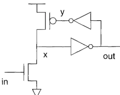
The first pulsed asynchronous circuit that we shall investigate is the "pulse repeater." A pulse repeater copies input pulses to its output. While this function could be performed by a wire or an open-loop amplifier, the pulse repeater has feedback; llsing the feedback, it restores the quality of the signals, both in the time domain and the voltage domain.
x
out
i;-1
Figure 3.1: Three-stage pulse repeater.
The circuit in Figure 3.1 is a simple three-stage pulse repeater. In its idle state, both the input and the output are at a logic zero, and the internal node :1: is at a logic one; this is the only stable
state of the circuit. When the input voltage is raised towards a logic one, the voltage on x begins to fall; which then causes 07J,t to rise, and finally, at least if in has meanwhile returned to zero, x
to rise back to the idle state. The circuit can misbehave if in remains at a logic one for too long. Characterizing the misbehavior and finding ways of avoiding it are the main topic of the rest of this chapter.
17
3.2.1
Timing constraints in the pulse repeater
The pulse repeater is a difficult circuit to get working reliably, owing to the timing assumptions that are necessary for verifying its correctness. If we will ensure that a pulse on in is noticed by the repeater, we must arrange that its length4 exceed some minimum. On the other hand, the pulse must not be too long; if it is, then the circuit may produce multiple outputs for a single input. (Depending on device strengths, it may instead stretch the output pulse. We might endeavor to design a pulse repeater so that this stretching could be used to keep the circuit reliable even with arbitrarily long input-pulses. Owing to the difficult design problems posed by the transistor-ratioing constraints, designing a reliable pulse repeater along these lines is difficult.)
We shall not consider the possibility that two input pulses arrive so close together that they appear as a single pulse-for two reasons: first, the problem of the pulses' arriving too close together can be understood similarly to how we understand the single too-short and too-long pulses; secondly, we shall see that the issue is not of much concern in the APL circuit-family because the pulse-handshake protocols require inserting an acknowledgment of some sort between the two pulses (i.e., we ensure at a higher level of the design that we never have two pulses sent without the target's responding with an acknowledgment in between).
x
out
i;-1
Figure 3.2: Five-stage pulse repeater.
3.2.2
Simulating the pulse repeater
The author has simulated a few variants of the pulse-repeater design described above with input pulses of varying lengths and heights applied, thus illustrating the timing margins of the pulse repeater. The repeaters that were simulated are similar to the simple three-stage version described above. The differences are that the input and output were negative-logic (i.e., the input transistor
18
is a p-transistor) and that "keeper" resistors were used on the x nodes. We shall see the results for two separate circuit designs: a three-stage version, and a five-stage version that differs only in two extra inverters' being used in the feedback path from x to y (Figure 3.2). The author produced layout for the pulse repeaters using the magic layout editor and simulated them with the aspice circuit simulator. The assumed technology is HP's O.6-ILm CMOS via MOSIS; the supply voltage,
V dd, is 3.3 volts for all simulations present(~d in this thesis. ,S
In what follows, we shall mainly aim at understanding the behavior of a single pulse traveling down an infinite chain of pulse r·epeater>8. Will t.lw Imlse die down? Will it lengthen until it becomes several pulses? Or will it~as we hope~travel down the chain unscathed?
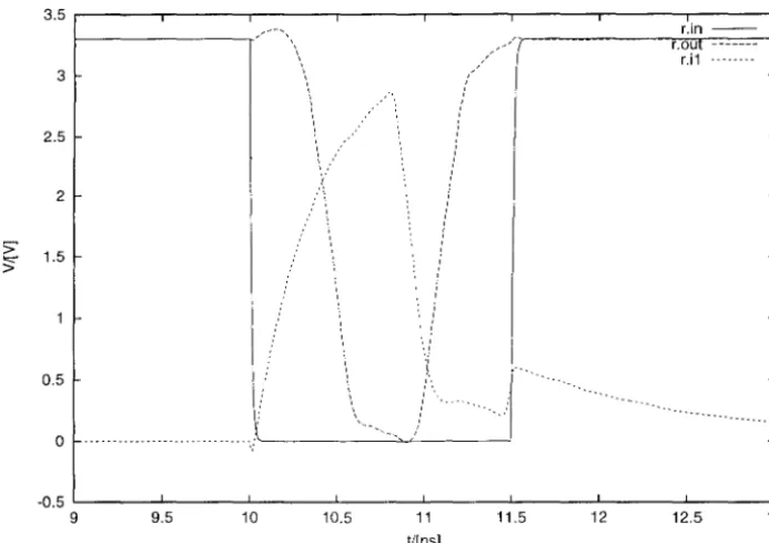
Two things can go wrong with the pulse repeater. The input pulse can be too weak for the circuit to detect it, or the input pulse can be of such long duration that it is detected as multiple pulses. An example of a pulse repeater on the verge of misbehaving owing to a too-long input pulse is shown in Figure 3.3. The nodes are labeled as follows: input, T.in; internal node, T.il; output, T.out; their senses are inverted compared with the pulse repeaters in the text. Here the input pulse is 1.5 ns long, beginning at t =10 ns. As we can see from t.he graph, the internal node T.il starts rising almost instantly, causing the output to fall about 20D ps later. At t = 11 nfl, the internal node rises again, thus re-arming the circuit. Slightly before t
=
11.5 ns, the re-armed circuit starts detectingthe input~which has by now overstayed its welcome~as a second pulse, but the detecting transistor
is cut off by the input, which falls back to GND barely in time to avoid being double-latched. Figure 3.4 shows the results of applying pulses of varying lengths and heights to the three-stage pulse repeater. The pipe-shaped region shows when a single input pulse results in a single output pulse, as desired. The other two regions correspond to forms of misbehavior: the region to the right of the pipe shows when a single input puls() results in several output pulses, i.e., when the input pulse is too long to be properly detected as a single pulse; the region to the left of the pipe shows when the input pulse is too feeble to elicit any response at all. (The gaps in the plot are due to irrelevant practical difficulties with the simulatiomi.)
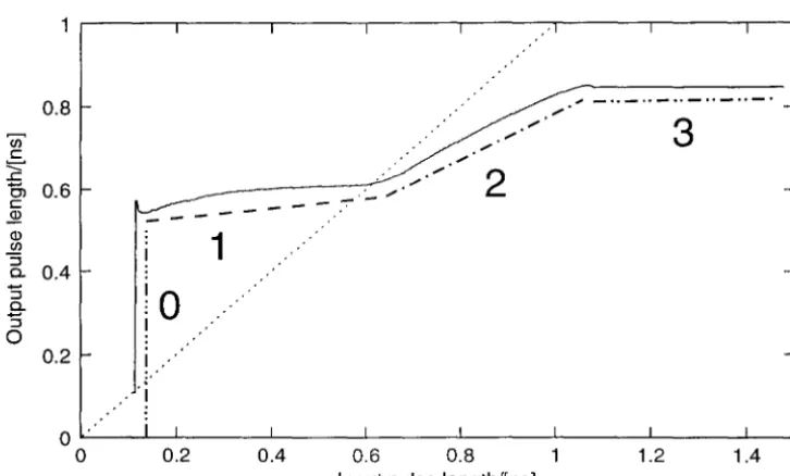
Figure 3.5 shows the results for the five-stage pulse repeater. Figure 3.6 shows a plot for the five-stage pulse repeater of the length of the output pulse for different lengths of the input pulse, the input swing here being from GND to Veld. The solid line shows the data; "0," "1," "2," and "3" indicate operating regions explained below. The diagonal dashed line in Figure 3.6 denotes the stability constraint that the output pulse is as long as the input pulse; we should expect that in an infinite chain of pulse repeaters, the pulses will eventually have the parameters implied by the intersection of the input-output curve and the stability constraint.6
5The parameters used are known to be inaccurate. The circuit speeds indicated by the simulations are 15-20 percent higher than what one can reasonably expect from fabricated parts. These parameters keep the simulations straightforwardly comparable with most of the work done ill the Caltech group in the last five years.
~
.<=
.!2' Q)
.<=
Q)
V)
"3
0-:;
0-s:
19
0.5
o ... .
. 0.5 " - - - ' - - - ' - - - ' - - - ' - - - ' - - - ' - - - ' - - - ' 9
3.5
3
2.5
2
1.5
0.5
9.5 10 10.5 11 tJ[ns]
11.5 12 12.5
Figure 3.3: A long pulse almost triggers a pulse repeater twice.
13
O~---~---~---L---L---~---~---L_~
o 0.2 0.4 0.6 0.8 1.2 1.4
Input pulse length/[ns]
3.5
3
2.5
~
""
2.9' CD
""
OJ<J) :5
c. 1.5
'5 c.
.E
0.5
o*---~---L---~---~
o 0.5 1.5 2
Input pulse length/[ns]
Figure 3.5: Shmoo plot for fivc-stage pulse repeater.
0.8
....
....
,._
..-
.._
.._
.._
.. -.3
Iii'
....
....
c
....
"'=:'
....
2
..c
....
"5l 0.6 . ....
c
- - -
..,..-~
-Q)
1
CIl"S 0. 0.4
"S
0
0.
"S
0
0.2
I 0
0 0.2 0.4 0.6 0.8 1.2 1.4
Input pulse length/[nsj
21
3.2.2.1 Analysis of pulse repeater data
There are two important questions we should ask when analyzing the pulse repeater data: First, can we cascade the circuits-can we connect them so that they work properly when the output of one is the input of another'? Secondly, do the circuits work over a reasonable range of parameter variations?
The "shmoo" plots, Figure 3.4 and Figure 3.5, are caricatured in Figure 3.7.7 Normally, if the
input pulse is of a reasonable height and length (see below), t.hen the gain of the pulse repeater will force the output pulse to be approximately characterized by t.he point. marked "X" in the caricature. Furthermore, the line "A" describes the minimum pulse length t.hat can be detected by the pulse repeater. This is set by circuit parameters, mainly by t.he strength of the input transistor and the load on its output. The other line, "B," marks t.he longest. pulse length that. will lead to a single output pulse.
The reason there is a maximum lengt.h t.hat. the repeat.er will not work properly beyond is that the repeater "double-latches" when the input. pulse is so long t.hat it is still present when the repeater has gone through the entire cycle x-L-; ... y-L-; :rt; ... yt; furthermore, the up- and down-going behaviors of the pulse repeater are roughly similar; t.he salIle numher of transitions is exercised, through roughly similar circuitry. Taken t.oget.her, this means t.hat the interval .T.!-; y.!-; xt (approximately the same length as the output pulse) is about t.he same lengt.h as t.he interval xt; yt; x-L-, where the final x-L-is the mx-L-isfiring resulting from the too-long input pulse. Hence, t.he pulse length along "B" will be about twice the length of the normal pulse "X."
3.2.2.2 Digital-analog correspondence
If we restrict ourselves to the digit.al domain, we can underst.and the pulse repeater's behavior for different input pulse lengths by considering the input pulse as two t.ransit.ions int; in.!-. The length of the input pulse is the length of the time interval bet.ween int and inl int begins the operation of the pulse repeater; leaving out in.!-, the sequence of t.ransit.ions is
int; x-L-; outt; y-L-; xt; out-L-; yt .
Changing the input pulse length amounts t.o changing the position of in-L- in this trace (we are here assuming that the sequence continues even in the absence of in-L-; i.e., in the presence ofinterference). There are five main possibilities:
O. in-L-occurs so early that the pulse on in is t.oo short t.o trigger the pulse repeater-t.hen t.here will be no sequence x-L-; O'll,tt; etc. The repeater fails.
impatient reader is urged to take a peek at Section :3.3 and t.heu to return here.
1. in-J,. occurs long enough after int that the input pulse is noticed, but it occurs before y-J,.. This is the ideal situation. There is no interference. The repeater works perfectly.
2. in-J,. occurs during y+- There is some interference, but because the input behavior is monotonic (the inputs tend to drive :r: strictly more towards Vild as time goes by), the interference is fairly harmless-a slig"htly lengthened output pulse may result. The repeater still works.
3. in-J,. occurs after y-J,. but not long enough after it to trigger the repeater again. The repeater still works, but it draws a great deal of short-circuit current.
4. in-J,. occurs long enough after y-J,. that :r:t has already occurred; x-J,. is triggered again, and the repeater generates a second output pulse. The repeater fails.
We may draw an analog connection: the possibilities 0.-3. correspond to the so labeled segments of Figure 3.6 (the part of the curve for possibility 4. is not shown). In normal operation, the repeater is thus operating at the border between possibilities 1. anel 2. This is not surprising, since the input pulse is approximately the same length as the resetting pulse on y.
3.2.2.3 The cascaded repeater
::r
CD
cO'
::r
~
'<
...
A
B
x
I
-I - - - -I -
-:--:-::-:---::-::-=--=-=-'""=-~-~~---input length/[ns]
Figure 3.7: Qualitative interpretation of shmoo plots.
Vdd
F
characteristics of the input pulse? Yes, it is. We can see this8 from Figure 3.6. This figure shows
that, in this fabrication technology, for input pulse lengths in the wide range from 0.12 to 1.47 ns, the output pulse lengths range only from 0.57 to 0.85 ns. (Note that the scale along the abscissa is not the same as that along the ordinate.) Since five transitions take about 0.61 ns here, we can say that in technology-neutral terms, the input pulse lengths may vary from about 1.0 normal transition delays to about 12 delays for an output variation from 4.7 to 7.0 delays.
Since the range of input pulse lengths comfortably contains the range of output pulse lengths, we should have to add considerable load, or we should have to fall victim to extreme manufacturing variations to make the pulse either die out or double up as it travels down a pipeline of pulse repeaters of this kind. Since, further, the input-output relationship of the pulse lengths is almost entirely monotonic, we can summarize the behavior of the pulse repeater thus: an input pulse of length between about 1.0 and 12 transition-delays will generate a single legal output pulse; the length gain averages 4.8.
~~
/~
input
\~
pulse length/[ns]
Figure 3.8: Mapping of input to output pulse parameters.
Figure 3.8 is another caricature of the operation of pulsed circuits. The input pulses within the input pipe lead to output pulses within the indicated output region.9
8Note that the various shmoo plots and the width-p;ain plot are drawn for several different circuits, so the numerical values are not necessarily directly comparable across them; ,L1so the criterion for a pulse's being legitimate is somewhat over-strict in the shmoo plots. We shall formalize the conditions later.
3.2.3
The synchronous digital model
The correctness of synchronous digital logic is justified by a two-part model that is familiar to every electrical engineering undergraduate. The first part explains what it means to be a valid logic-level by dividing the possible analog voltages of a digital circuit into a few ranges with the right properties to guarantee that noise is rejected; this division we call the digital logic-Ie vel-discipline , 10
or logic discipline for short. The second part introduces a synchronous timing-discipline. The timing discipline can be introduced in several ways, which all rely on defining the times when circuit elements are allowed to inspect the analog voltages (i.e., when they can be proved to obey the logic discipline) and defining the times when the circuit may change the voltages (when the voltages cannot be shown to obey the logic discipline of the model). The timing discipline is normally maintained by introducing latches and a clock and specifying setup and hold times for the latches. Comparing Figure 3.8 with the synchronous logic-discipline, we can identify the big pipe with the legal input-range for a logic value; the little pipe, with the legal output range; the difference between the two is, intuitively speaking, the noise margin.
The synchronization behavior of asynchronous circuits is sufficiently different from the syn-chronous timing-discipline that we shall have to develop a different timing model. The synsyn-chronous logic-discipline, on the other hand, rests on a transitive-closure property of synchronous digital cir-cuits that we may emulate for deriving sufficient conditions for the correctness of APL circir-cuits. In the synchronous world, introducing legal-voltage ranges and noise margins establishes the correct-ness of the digital model; having introduced these constructs, we can show that voltages that have clear digital interpretations will be maintained throughout a circuit as long as the noise that is present is less than the noise margins [84]. We shall generalize this one-dimensional model for the asynchronous pulses.
3.2.4
Asymmetric pulse-repeaters
We noted above (Section 3.2.2.2) that the pulse repeater normally operates on the border between the "ideal" domain and the "fairly harmless" clomaill. The reason for this is that, in a long chain of cascaded inverters, the reset pulse on y is about the same length as the input pulse on in.
Practically speaking, there is interference in tht~ "fairly harmless" domain; this means that the circuit generates extra noise and uses more power than necessary. Furthermore, many theoretical difficulties are caused by this interference, as we shall see below. Is there no way of avoiding this?
In fact, it is fairly easy to avoid the 'in pulse's interfering with the y pulse. What we need is a circuit that generates pulses of different lengths on y and 011,t; the pulse on out needs to be shorter
shall touch the input shape. Hence, the pipe Rhown in Figure 3.8 is actually a little smaller than the ones shown in Figures 3.4 and 3.5 (by about 1/5).
25
than the one