ISSN(Online): 2320-9801 ISSN (Print): 2320-9798
I
nternational
J
ournal of
I
nnovative
R
esearch in
C
omputer
and
C
ommunication
E
ngineering
(An ISO 3297: 2007 Certified Organization)
Vol. 3, Issue 5, May 2015
Low Power, Area Efficient & High
Performance Carry Select Adder on FPGA
Bagya Sree Auvla, R.Kalyan
M. Tech Student , Dept. of ECE, Swetha Institute of Technology & Science, JNTUA, Tirupati, India
Assistant professor, Dept.ECE, Swetha Institute of Technology &Science, JNTUA, Tirupati, India
ABSTRACT: LOW-POWER, area-efficient, and high-performance VLSI systems are increasingly used in portable and mobile devices, multi standard wireless receivers, and biomedical instrumentation. An adder is the main component of an arithmetic unit. A complex digital signal processing (DSP) system involves several adders. An efficient adder design essentially improves the performance of a complex DSP system. A ripple carry adder (RCA) uses a simple design, but carry propagation delay (CPD) is the main concern in this adder. Carry look-ahead and carry select (CS) methods have been suggested to reduce the CPD of adders. A conventional carry select adder (CSLA) is an RCA configuration that generates a pair of sum words and output carry bits corresponding the anticipated input-carry (cin = 0 and 1) and selects one out of each pair for final-sum and final output-carry . A conventional CSLA has less CPD than an RCA, but the design is not attractive since it uses a dual RCA. In the existing designs, logic is optimized without giving any consideration to the data dependence. In this paper, we prepared an analysis on logic operations occupied in conventional and BEC-based CSLAs to study the data dependence and to identify redundant logic operations. Based on this study, we have planned a new logic formulation for the CSLA. The major contribution in this paper is logic formulation based on data dependence and optimized carry generator (CG) and carry select unit Based on the proposed logic formulation, we have found a capable logic design for CSLA. Due to better logic units, the projected CSLA involves significantly less ADP than the existing CSLAs. We have shown that the SQRT-CSLA using the proposed CSLA design involves nearly 32% less ADP than that of the corresponding SQRT-CSLA.
KEYWORDS: XOR gate, Carry Select Adder, FPGA, Digital Signal Processing, BEC.
I. INTRODUCTION
Carry Select Adder (CSLA) is one of the fastest efficient adders which are used in many data-processing processors to perform fast arithmetic functions. CSLA is called efficient adder because of less delay and reduced size. Since, area is the major constraint which plays a vital role in integrated circuits. From the structure of the CSLA, it is clear that there is scope for reducing the area and power consumption in the CSLA. The proposed work conveys that it uses a simple and efficient gate-level modification to significantly reduce the area and power of the CSLA. Based on this modification 8-, 16-, 32-, and 64-b square-root CSLA (SQRT CSLA) architecture have been developed and compared with the regular BEC SQRT CSLA architecture. The proposed design has reduced area and power as compared with the regular BEC SQRT CSLA. The proposed design has lesser area owing to the modifications in the BEC unit by gate reduction due to combinational logic. The performance factors of the proposed design are evaluated in terms of delay, area, power and their products by simulation tool and implemented in FPGA kit.
ISSN(Online): 2320-9801 ISSN (Print): 2320-9798
I
nternational
J
ournal of
I
nnovative
R
esearch in
C
omputer
and
C
ommunication
E
ngineering
(An ISO 3297: 2007 Certified Organization)
Vol. 3, Issue 5, May 2015
isting SQRT-CSLA designs, on average, for different bit-widths. The application specified integrated circuit (ASIC) synthesis re-sult shows that the BEC-based SQRT-CSLA design involves 48% more ADP and consumes 50% more energy than the proposed SQRT-CSLA, average, for different bit-widths. In this brief, the logic operations involved in conventional carry select adder (CSLA) and binary to excess-1 converter (BEC)-based CSLA are analysed to study the data dependence and to identify redundant logic operations. We have eliminated all the redundant logic operations present in the conventional CSLA and proposed a new logic formulation for CSLA. In the proposed scheme, the carry select (CS) operation is scheduled before the calculation of final-sum, which is different from the conventional approach. Bit patterns of two anticipating carry words (corresponding to cin = 0 and 1) and fixed cin bits are used for logic optimization of CS and generation units. An efficient CSLA design is obtained using optimized logic units. The proposed CSLA design involves significantly less area and delay than the recently proposed BEC based CSLA. Due to the small carry-output delay, the proposed CSLA design is a good candidate for square-root (SQRT) CSLA. A theoretical estimate shows that the proposed SQRT-CSLA involves nearly 35% less area–delay–product (ADP) than the BEC-based SQRT-CSLA, which is best among the existing SQRT-CSLA designs, on average, for different bit-widths. The application specified integrated circuit (ASIC) synthesis result shows that the BEC-based SQRT-CSLA design involves 48% more ADP and consumes 50% more energy than the proposed SQRT-CSLA, on average, for different bit-widths. RCA due to the anticipation of both possible CIN values of in advance, and as the multiplexers is used for the selection of ϹIN , so the area increases as compared to RCA. The propagation time through the Carry Select Adder is calculated using following mathematical equation:
Fig: System architecture
II. LITERATURE SURVEY
ISSN(Online): 2320-9801 ISSN (Print): 2320-9798
I
nternational
J
ournal of
I
nnovative
R
esearch in
C
omputer
and
C
ommunication
E
ngineering
(An ISO 3297: 2007 Certified Organization)
Vol. 3, Issue 5, May 2015
increment adder, carry save adder and carrybypass adder. The module functionality and performance issues like area, power dissipation andpropagation delay are analyzed at 0.12μm 6metal layer CMOS technology using micro wind tool.
III.EXISTING SYSTEM
Carry Select Adder (CSLA) In RCA every full adder has to wait for the incoming carry before an outgoing carry is generated. One way to get around this linear dependency is to anticipate both possible values of the carry input i.e. 0 and 1 and evaluate the result in advance. Once the real value of the carry is known the result can be easily selected with the help of a simple multiplexer stage. Figure 1 Block Diagram of Carry Select Adder A 16-bit CSLA is constructed by dividing into 4 stages i.e. N=16 total number of bits, M=4 number of bits per stage, (N/M = 4) and chaining such four equal length blocks as shown in Figure 1.6. CSA has less delay as compared to M U M U M U 0 0 0 0 C C C C C SUM[ SUM[1 SUM[ SUM[ SUM 15:11 10:7 6:4 3:2 1:0 A[15: B[1 A[1 B[1 A[ B[ A[3 B[3:2] A[ B[ M U MODIF IED 6 MODIF IED 3 MODIF IED 4 MODIF IED 5 RCA due to the anticipation of both possible values of in advance, and as the multiplexers is used for the selection of , so the area increases as compared to RCA. The propagation time through the Carry Select Adder is calculated using following mathematical equation: Where, is delay of the setup stage to produce propagate and generate signals, is the time taken by the carry to ripple through a length of the stage M , is the delay of the multiplexer stage and is sum of time. The existing system uses BEC instead of RCA with carry in 1 in the regular CSLA to achieve lower area. With an efficient design of an add-one circuit, the power and area of CSA can be reduced. But the XOR function in BEC consists of five gates according to the previous design. The Figure 2 shows the existing BEC circuit and the Figure 3 shows the existing XOR function. Figure 2 Existing 4-bit BEC circuit A B Figure 3XOR Logic Table I Gate Requirements of Existing System
IV.MODIFIEDSYSTEM
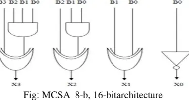
Modified BEC Structure CSLA Area XOR 5 2:1 MUX 4 HA 6 FA Above diagram clearly shows the modified BEC structure of the SQRT CSLA. It has reduced area compare than basic BEC structure of the SQRT CSLA. Below table indicates the area reduction of modified BEC structure of SQRT CSLA. Table II Gate Requirements of Proposed System CSLA Area XOR 4 2:1 MUX 4 HA 6 FA 13 MODIFIED CARRY SELECT ADDER (MCSA) DESIGN A Modified Carry Select-Adder (MCSA) design is proposed, which make use of single RCA and Binary to Excess-1 Converter (BEC) instead of using dual RCAs to reduce area and power consumption with small speed penalty. The reason for area reduction is that, the number of logic gates used to design a BEC is less than the number of logic gates used for a RCA design.
Fig
:
MCSA 8-b, 16-bitarchitecture
ISSN(Online): 2320-9801 ISSN (Print): 2320-9798
I
nternational
J
ournal of
I
nnovative
R
esearch in
C
omputer
and
C
ommunication
E
ngineering
(An ISO 3297: 2007 Certified Organization)
Vol. 3, Issue 5, May 2015
bit, 32-bit and 64-bit its area, power and delay are analyzed. The results so obtained are then compared with the results of conventional CSA.
Fig: Modified MCSA 16-bit, 32-bit
X0= ~𝐵0
X1=B0(1)^𝐵1
X2=B2^(B0&B1) X3=B2^(B0&B1&B2)
CSLA
AREA
XOR
5
2:1 MUX
4
HA
7
FA
12
Table 1: CSLA measurement table
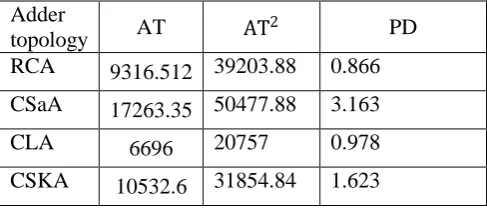
Table 1 presents the performance analysis of different adder topologies. Table 2 presents the parameters of AT, AT2 and PD values of adders. the energy delay and parasitic extraction values. All the adders are simulated with multiple design corners (TT, FF, FS, and SS) to verify that operation across variations in device characteristics and environment. To establish an unbiased testing environment, the simulations have been carried out using a comprehensive input signal pattern, which covers every possible transition for all the adders.
Adder
topology
AT
AT
2
PD
RCA
9316.512 39203.88
0.866
CSaA
17263.35 50477.88
3.163
CLA
6696
20757
0.978
CSKA
10532.6
31854.84
1.623
Table 2 AT, AT2 and PD values of Adders
ISSN(Online): 2320-9801 ISSN (Print): 2320-9798
I
nternational
J
ournal of
I
nnovative
R
esearch in
C
omputer
and
C
ommunication
E
ngineering
(An ISO 3297: 2007 Certified Organization)
Vol. 3, Issue 5, May 2015
Fig: Modified CSA 32-bit BEC
V. RESULTSANDDISCUSSIONS MICROWIND:
Tool which is chosen to simulate this scheme is microwind & DSch Version2.DSCH stands for Digital Schematic.
DSCH2:
The DSCH2 is a logic editor and simulator.DSCH2 is used to validate the architecture of logic circuit before the microelectronics design is started.DSCH2 provides user friendly environment for hierarchical logic design and simulation with delay analysis which allows the design and validation of complex logic structures. A key innovative future is the possibility to estimate the power consumption of the circuit.
MICROWIND:
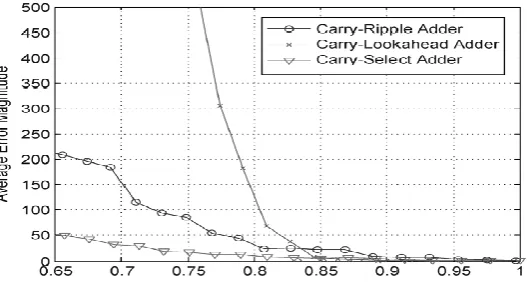
MICROWIND2 Program allows the student to design and simulate an integrated circuit at physical description level. The package contains the library of common logic and analog ICs to view and simulate.MICROWIND2 includes all the commands for a mask editor as well as original tools never gathered before in a single module. Gain of this tool is access the circuit simulation by pressing a single key. The electric extraction of the circuit is automatically performed and the analog simulator produces voltage and current curves immediately. With 16-b adder design as an example, this section shows that different computer arithmetic architectures may respond to
Fig . Simulated average error magnitude versus normalized power consumption for the three 16-b adders operating at 800 MHz
ISSN(Online): 2320-9801 ISSN (Print): 2320-9798
I
nternational
J
ournal of
I
nnovative
R
esearch in
C
omputer
and
C
ommunication
E
ngineering
(An ISO 3297: 2007 Certified Organization)
Vol. 3, Issue 5, May 2015
First, to evaluate the propagation delay versus supply voltage characteristic of the TSMC 65-nm standard cell library, we carried out simulations on a 1-b full adder (with a load of an inverter with ten times minimum size), as shown in Fig. 1. It shows that the propagation delay is almost linearly proportional to the supply voltage.We further carried out simulations on the aforementioned three 16-b adders under different supply voltages while fixing the frequency as 800 MHz. For each simulation run, we randomly generated 10 6 pairs of 16-b input data, where each bit has equal probability to be 0 or 1 and all the bits are randomly generated independent from each other. Fig. 2 shows the simulated average error magnitude versus normalized power consumption, where the average error magnitude is the mean of the computation error magnitude over all the simulated samples and the power consumptions are normalized against the highest power consumption among all the adders under a normal supply voltage. Fig. 3 shows the simulated average bit error rate (i.e., the number of bits that is wrongly computed) versus normalized power consumption. It shows that, under an overscaled supply voltage, the carry-ripple adder has the least bit error rate, while the carry-select adder has the least performance degradation if we take into account the significance of each output bit. Although all the adders have similar bit error rates (i.e., 0.06–0.14), they have very different average error magnitudes, as shown in Fig. 2. Since the performance degradation of signal processing systems under an overscaled voltage heavily depends on the computation error magnitude, the aforesaid results suggest that we should not use mere computation bit error rate as a metric to select the appropriate arithmetic architecture and that we should be able to directly estimate the average error magnitude characteristics for each candidate arithmetic architecture.
Fig:Error Significance Fig:Factor Assignment
The error significance factor associated with each internal signal in computer arithmetic circuits represents the maximum computation output error magnitude that is incurred if the present internal signal cannot propagate to the output bits in time. For example, let us again consider the 8-b unsigned carry-select adder, as shown in Fig. 5. As discussed previously, if a switch on the carry-select signal cannot propagate to the four MSBs in time, the output error magnitude is . Hence, we have that the error significance factor of the carry-select signal is eight. Motivated by this example, we have the following simple rules to determine the error significance factor of each internal signal:
1) If an internal signal only contributes to one computation output bit, then its error significance factor is assigned as the weight of the corresponding output bit.
2) If an internal signal contributes to a group of computation output bits, then its error significance factor is assigned as the minimum one among the weights of the output-bit grou
VI.CONCLUSION AND FUTURE WORK
ISSN(Online): 2320-9801 ISSN (Print): 2320-9798
I
nternational
J
ournal of
I
nnovative
R
esearch in
C
omputer
and
C
ommunication
E
ngineering
(An ISO 3297: 2007 Certified Organization)
Vol. 3, Issue 5, May 2015
size up to 128-bit can be designed and implemented in FPGA Board design. Then the CSLA can be implemented in Multiplier and Filter applications and its speed of operation is evaluated.
REFERENCES
1. Anjum Asma and Gihan Nagib,’Energy Efficient Routing Algorithms for Mobile Ad Hoc Networks–A Survey’, International Journal of Emerging Trends & Technology in computer Science, Vol.3, Issue 1, pp. 218-223, 2012.
2. Hong-ryeol Gil1, Joon Yoo1 and Jong-won Lee2 ,’An On-demand Energy-efficient Routing Algorithm for Wireless Ad hoc Networks’, Proceedings of the 2nd International Conference on Human. Society and Internet HSI'03, pp. 302-311, 2003.
3. S.K. Dhurandher, S. Misra, M.S. Obaidat, V. Basal, P. Singh and V. Punia,’An Energy-Efficient On Demand Routing algorithm for Mobile Ad-Hoc Networks’, 15 th International conference on Electronics, Circuits and Systems, pp. 958-9618, 2008.
4. DilipKumar S. M. and Vijaya Kumar B. P. ,’Energy-Aware Multicast Routing in MANETs: A Genetic Algorithm Approach’, International Journal of Computer Science and Information Security (IJCSIS), Vol. 2, 2009.
5. AlGabri Malek, Chunlin LI, Z. Yang, Naji Hasan.A.H and X.Zhang ,’ Improved the Energy of Ad hoc On- Demand Distance Vector Routing Protocol’, International Conference on Future Computer Supported Education, Published by Elsevier, IERI, pp. 355-361, 2012.
6. D.Shama and A.kush,’GPS Enabled E Energy Efficient Routing for Manet’, International Journal of Computer Networks (IJCN), Vol.3, Issue 3, pp. 159-166, 2011.
7. Shilpa jain and Sourabh jain ,’Energy Efficient Maximum Lifetime Ad-Hoc Routing (EEMLAR)’, international Journal of Computer Networks and Wireless Communications, Vol.2, Issue 4, pp. 450-455, 2012.