Nonisolated High Voltage Gain DC-DC
Converters Based on SSC and VMC
S.Prakash, S.P.Vijayaragavan, Dr. K. N. Bhanuprakash
Associate Professor, Dept. of EEE, Bharath University, Chennai, Tamil Nadu, India
Assistant Professor, Dept. of EEE, Bharath University, Chennai, Tamil Nadu, India
Professor, Dept. of EEE, Bharath University, Chennai, Tamil Nadu, India
ABSTRACT: This paper is about a new dc-dc converter based on VOLTAGE MULTIPLIER CELL and MULTI STATE SWITCHING CELL. This method can be applied for all type of converters like BUK, BOOST,BUK-BOOST,CUK,SEPIC &ZETA. To verify the operating principle BOOST converter is chosen. Experimental analysis is obtained from 1Kw lab prototype and the results are verified using simulation software. The output current and voltage waveforms are analyzed experimentally using the digital oscilloscope. The experimental results are compared with the results obtained from the software analysis using the matlab software. The analyzed converter can be applied in uninterruptible power supplies, fuel cell systems, and is also adequate to operate as a high-gain boost stage with cascaded inverters in renewable energy systems. Furthermore, it is suitable in cases where dc voltage step-up is demanded, such as electrical fork-lift, audio amplifiers, and many other applications.
I. INTRODUCTION
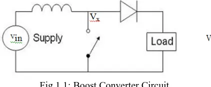
This paper introduces a dc–dc converter based on the three-state switching cell and voltage multiplier cells. In order to verify the operation principle of this converter, the boost converter is chosen and experimented in detail.[1-2] The behavior of the converter is analyzed through theoretical analysis, while its performance is investigated by experimental results obtained from matlab simulation. The analyzed converter can be applied in uninterruptible power supplies, fuel cell systems, and is also adequate to operate as a high-gain boost stage with cascaded inverters in renewable energy systems. Furthermore, it is suitable in cases where dc voltage step-up is demanded, such as electrical fork-lift, audio amplifiers, and many other applications. [3]A DC-to-DC converter is a device that accepts a DC input voltage and produces a DC output voltage. Typically the output produced is at a different voltage level than the input. In addition, DC-to-DC converters are used to provide noise isolation, power bus regulation, etc. A review on Converters, firstly schematic showed in Fig. 1.1 shows the basic boost converter.
Fig 1.1: Boost Converter Circuit
This circuit is used when a higher output voltage than input is required.
While the transistor is ON Vx =Vin, and the OFF state the inductor current flows through the diode giving Vx =Vo. For
this analysis it is assumed that the inductor current always remains flowing (continuous
Fig 1.2 Voltage and Current Waveform
Since the duty ratio "D" is between 0 and 1 the output voltage must always be higher than the input voltage in magnitude. The negative sign indicates a reversal of sense of the output voltage.[4]
ISOLATED DC-DC CONVERTERS
In many DC-DC applications, multiple outputs are required and output isolation may need to be implemented depending on the application. In addition, input to out put isolation may be required to meet s afety standards and to provide impedance matching. The above-discussed DC- DC topology can be adapted to provide iso lation between input and output.[5-7]
FLY BACK CO NVERTER
The flyback converter can be developed as an extension of the Buck-Boost converter. Fig 1.3 shows the basic converter; Fig 1.4 replaces the inductor by a transformer. The buck-boost converter works by storing energy in the inductor during the ON phase and releasing it to the output during the OFF phase.[8]
Fig 1.3 Buck Boost Converter
Fig 1.4 Inductor Replaced by Transformer
Fig 1.5 FlyBack Converter
Converters with ma gnetically coupled inductance such as flyback or the single-ended primary inductance converter (SEPIC) can easily achieve high voltage gain using switches with reduced on-resistance, even though efficiency is compromised by the losses due to the leakage inductance. An active clamping circuit is able to regenerate the leakage energy, at the cost of increased complexity and some loss in the auxiliary circuit .The efficiency of the conventional flyback structure is typically low due to the parasitic inductance. A possible solution lies in connecting the output of the boost converter to that of the flyback topology, with consequent increase of voltage gain due to the existent coupling between the arrangements. In this case, the boost convert behaves as an active clamping circuit when the main switch of the flyback stage is turned OFF.
The drawbacks of the conventional circuit is Large in size due to bulky inductor and capacitor, Less efficiency, More voltage stress, Complex control circuit, More Power Losses.
II. PROPOSED METHODOLOGY
The converter proposed has high voltage gain, while the input current is continuous with reduced ripple. The input inductor is also designed for twice the switching frequency, implying reduction of weight and size. The voltage stress through the switches is less than half of the output voltage due to clamping performed by the output filter capacitor. It is also important to mention that, for a given duty cycle, the output voltage can be increased by adjusting the transformer turns ratio without affecting the voltage stress across the main switches.
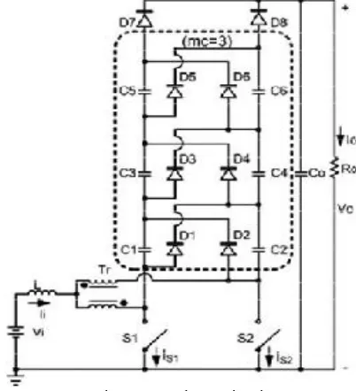
Fig 1.5 Proposed Circuit Diagram
Three state switching cell and voltage multiplier cell is interleaved into the boost converter. Three state switching cell consist of two diodes, coupled inductor and two MOSFETs. Voltage multiplier cell consist of diodes and capacitors connected in parallel. The 3SSC and VMC can be interleaved into main circuit without disturbing the main circuit. A n number of voltage multiplier cell can be added to the circuit according to the requirement of voltage. [10-12]
remain in off condition. During this mode diode D1, D3, D5 are forward biased and conducts through D8 capacitors C2, C4, C10 are charged while all the remaining capacitors are discharged. Third and fourth mode of operation is similar to that of first and second mode of operation. The use of high-voltage gain converters is of great interest, even though many approaches are based on Non- isolated topologies . This paper presents a topology for voltage step-up applications based on the use of multiplier cells constituted by diodes and capacitors.[13] The converter is able to operate in overlapping mode (when a duty cycle D is higher than 0.5) and nonoverlapping mode (when a duty cycle D is lowerthan 0.5). However, the study carried out in this paper only considers the operation with D > 0.5. The generic structure, which is valid for any number of cells, is initially presented, while the analysis is focused on structures with three cells, aiming to determine the stress regarding the elements that constitute the aforementioned configurations.Experimental results regarding the structure with three multiplier cells are also presented and discussed to validate the proposal. By using the proposed cell , it is possible to generate the six novel nonisolated dc–dc converters, i.e., buck, boost, buck–boost, Cuk, SEPIC, and zeta.The advantages of Reduced No of switches, Increased efficiency, Control Logic Reduces, Reduced losses. The boost converter is chosen to verify the claimed advantages of the converter family. The circuit considers the converter associated with 3State switching cell and three voltage multiplier cells.
The 3SSC is obtained by the association of two two-state switching PWM cells (2SSCs) interconnected to a center tap autotransformer. Some prominent advantages are reduced size, weight, and volume of magnetic, which are designed for twice the switching frequency.
Fig 1.6 Three state switching Cell
Fig 1.7 Voltage Multiplier Circuits
The voltage increases by cascading several voltage multiplier cells constituted by diodes and capacitors that operates on the resonance principle. The voltage stress across the elements is reduced due to clamping performed by the output capacitor. The high step up dc–dc converter with three state switching cell and voltage multiplier cells provides continuous input current with reduced ripples and high voltage.
Voltage multiplier cells (VMCs) are adopted to provide high voltage gain and reduce voltage stress across the semiconductor elements. Interleaving allows the operation of the multiplier stages with reduction of the current stress through the devices. Besides, the size of input inductors and capacitors is drastically reduced. The voltage stress across the main switches is limited to half of the output voltage for a single multiplier stage.
The figure shows the complete experimental circuit of the proposed DC-DC converter. For good operation of the VMC shown in Fig 1.6, ac input voltage is required, which is an important requirement of this cell. Due to this fact, the use of the 3SSC depicted in Fig 1.5 is considered because it generates such ac voltage across the terminals of the autotransformer and the drain terminals of the controlled switches. For this reason, both cells are integrated leading to the proposed cell shown in Fig1.7.
In the resulting cell, the controlled switches can be represented by MOSFETs, junction field-effect transistors, insulated gate bipolar transistors, bipolar junction transistors, etc. All the generated topologies present bidirectional characteristics. By using the proposed cell shown in Fig 2.4, it is possible to generate the six novel nonisolated dc–dc converters, i.e., buck, boost, buck–boost, C´uk, SEPIC, and zeta. The use of high-voltage gain converters is of great interest. It is worth to notice that the use of nonisolated converters particularly dedicated to applications regarding renewable power systems has been the scope of recent works . The efforts leading to the development of such nonisolated topologies are then well justified in the literature. In order to verify the claimed advantages of the converter family, the boost converter is chosen. The developed analysis considers the converter associated with three voltage multiplier cells and is detailed as follows.
MODES OF OPERATION
In order to better understand the operating principle of the structures, the following assumptions are made: the input voltage is lower than the output voltage;
steady-state operation is considered;
semiconductors and magnetics are ideals;
switching frequency is constant;
the turns ratio of the autotransformer is unity; the drive signals applied to the switches are 180◦
Mode 1 :
Switches S1 and S2 are turned ON, while all diodes are reverse biased. Energy is stored in inductor L and there is no energy transfer to the load. The
output capacitor provides energy to the load. This stage finishes when switch S1 is turned OFF.
Mode 2 :
Mode 3 :
Switches S1 and S2 remain turned OFF and ON, respectively. DiodesD3 andD7 are forward biased, while all the remaining ones are reverse biased. Energy is transferred to the output stage through D7 . The inductor stores energy, and capacitors C2 and C4 are still charged. Capacitors C1 is discharged, and so are C3 and C5 .
Mode 4 :
Switch S2 remains turned ON, diode D3 is reverse biased, and diode D1 is forward biased. Energy is transferred to the load through D7 . The inductor is discharged, and so are capacitors C1 , C3 , and C5 , while C2 is charged.
Mode 5 :
Mode 6 :
Switch S2 is turned OFF and switch S1 is still turned ON. Diode D6 is forward biased. The inductor is charged by the input source, although capacitors C2 and C4 are discharged instead.
Mode 7 :
Mode 8 :
Switch S1 is turned ON, while S2 remains. turned OFF. Diodes D2 and D8 are forward biased, while D4 is reverse biased as well as the remaining diodes. Energy transfer to the load occurs through D8 , and capacitor Co is still charged. The inductor is discharged, while capacitor C1 is charged and capacitors C2 , C4 , and C6 are discharged.
Characteristics of the Proposed System
STATIC GAIN
The static gain for the generic structure of the boost converter Can be obtained from the inductor volt–second balance. The Voltage area multiplied by the time interval that corresponds To the inductor charge is equal to that regarding the inductor Discharged. The following expression can then be derived:
Fig 1.8 Static Gain Curves
represented by the dotted line. It occurs because the multiplier capacitors are not fully charged due to the reduced charge time.
III. SIMULATION RESULTS
The fig 2.1 shown is the simulation diagram for the conventional boost converter. The supply is 300 volts. The duty cycle is set as 5 0%. The switching frequency is 10khz. Since it is a boost converter it will boost the voltage to two times the input voltage. So the above circuit will provide an output of 600 volts. The output can be verified from the simulation.
Fig 2.2 Output Voltage
For an input of 300 volts the boost convertor boosts up the voltage for switching frequency 10khz and duty cycle 50% to 600 volts.
IV. PROPOSED CIRCUIT
Fig 2.3 Simulation diagram for the proposed circuit.
Fig 2.4 Shows the Output Voltage waveform for an input voltage of 10 volts.
Fig 2.5 Shows the Current output Waveform for an input voltage of 10 Volts.
Hardware Prototype
Fig 2.5 Hardware Diagram
Fig 2.6 Trigger pulse to switch 1
V. PROTOTYPE OUTPUT
INPUT=10.1V OUTPUT=104.1V
VI. CONCLUSION
This paper has proposed six generalized nonisolated high gain voltage dc–dc converters. To verify the principle operation of the generated structures, the boost converter was chosen.An important characteristic that can be seen in the experimental results is the reduced blocking voltages across the controlled switches compared to similar circuits, allowing the utilization of MOSFETs with reduced on-resistance. The qualitative analysis, theoretical analysis, losses modeling, and experimental results for a 1-kW prototype have been discussed. The converter achieves about 95.3% efficiency at rated load if compared to similar configurations that were previously proposed in the literature. It is also expected that nonisolated converters based on the 3SSC and VMC may be competitive solutions for high-current-high-voltage-step-up applications if compared with some other isolated approaches. In this prototype a timer circuit is used to produce the trigger pulse to the mosfet. Instead of the timer circuit a microcontroller can be used to provide the trigger pulse. The microcontroller can provide a exact pulse with duty cycle less than 0.5 which helps to increase the efficiency and gain of the converter. Using the components of the same specification can provide more accurate results.
REFERENCES
[1] R. Kadri, J.-P. Gaubert, and G. Champenois, “An improved maximum power point tracking for photovoltaic grid-connected inverter based on voltage-oriented control,” IEEE Trans. Ind. Electron., vol. 58, no. 1, pp. 66–75, Jan. 2011.
[2]Subha Palaneeswari M., Abraham Sam Rajan P.M., Silambanan S., Jothimalar, "Blood lead in end-stage renal disease (ESRD) patients who were on maintainence haemodialysis", Journal of Clinical and Diagnostic Research, ISSN : 0973 - 709X, 6(10) (2012) pp.1633-1635.
[3]Sharmila S., Rebecca L.J., Saduzzaman M., "Effect of plant extracts on the treatment of paint industry effluent", International Journal of Pharma and Bio Sciences, ISSN : 0975-6299, 4(3) (2013) pp.B678-B686.
[4]M. Berkhout and L. Dooper, “Class-D audio amplifiers in mobile applications,” IEEE Trans. Circuits Syst. I, Reg. Papers, vol. 57, no. 5, pp. 992– 1002, May 2010.
[5]Jeyanthi Rebecca L., Dhanalakshmi V., Sharmila S., "Effect of the extract of Ulva sp on pathogenic microorganisms", Journal of Chemical and Pharmaceutical Research, ISSN : 0975 – 7384 , 4(11) (2012) pp.4875-4878.
[6]Sharmila D., Saravanan S., "Efficacy of lead on germination growth and morphological studies of Horse Gram (Dolichos biflorus Linn)", Journal of Chemical and Pharmaceutical Research, ISSN : 0975 – 7384 , 4(11) (2012) pp.4894-4896.
[7] E. K. Sato,M. Kinoshita, Y. Yamamoto, and T. Amboh, “Redundant highdensity high-efficiency double-conversion uninterruptible power system,” IEEE Trans. Ind. Appl., vol. 46, no. 4, pp. 1525–1533, Jul./Aug. 2010.
[8]Saduzaman M., Sharmila S., Jeyanthi Rebecca L., 'Efficacy of leaf extract of Moringa oleifera in treating domestic effluent", Journal of Chemical and Pharmaceutical Research, ISSN : 0975 – 7384, 5(2) (2013) pp.139-143.
[9]S. V. Araujo, R. P. Torrico-Bascope, and G. V. Torrico-Bascope, “Highly efficient high step-up converter for fuel-cell power processing based on three-state commutation cell,” IEEE Trans. Ind. Electron., vol. 57, no. 6, pp. 1987–1997, Jun. 2010.
[10]Z. Amjadi and S. S. Williamson, “Power-electronics-based solutions for plug-in hybrid electric vehicle energy storage and management systems,” IEEE Trans. Ind. Electron., vol. 57, no. 2, pp. 608–616, Feb. 2010.
[11]L. G. Junior,M. A. G. Brito, L. P. Sampaio, and C. A. Canesin, “Integrated inverter topologies for lowpower photovoltaic systems,” in Proc. Int.Conf.Ind. Appl., 2010, pp. 1–5.
[13] R. A. Da Camara, C. M. T. Cruz, and R. P. Torrico-Bascope, “Boost based on three-state switching cell for UPS applications,” in Proc. Brazilian Power Electron. Conf., 2009, pp. 313–318.
[14] Thooyamani, K.P., Khanaa, V., Udayakumar, R., "Wireless cellular communication using 100 nanometers spintronics device based VLSI", Middle - East Journal of Scientific Research, v-20, i-12, pp:2037-2041, 2014.
[15] Vanangamudi, S., Prabhakar, S., Thamotharan, C., Anbazhagan, R., "Dual fuel hybrid bike", Middle - East Journal of Scientific Research, v-20, i-12, pp:1819-1822, 2014.
[16] Udayakumar, R., Kaliyamurthie, K.P., Khanaa, Thooyamani, K.P., "Data mining a boon: Predictive system for university topper women in academia", World Applied Sciences Journal, v-29, i-14, pp:86-90, 2014.
[17] Satheesh, S., Lingeswaran, K., "High efficiencytransformer less inverter for single-phase photovoltaic systems using switching converter", Middle - East Journal of Scientific Research, v-20, i-8, pp:956-965, 2014.